Power Supply Supervisory Circuit
∑
Includes Over-voltage,
Under-voltage, And Current
Sensing Circuits
∑
Internal 1% Accurate
Reference
∑
Programmable Time Delays
∑
SCR "Crowbar" Drive Of
300mA
∑
Remote Activation Capability
∑
Optional Over-voltage Latch
∑
Uncommitted Comparator
Inputs For Low Voltage
Sensing (UC1544 Series
Only)
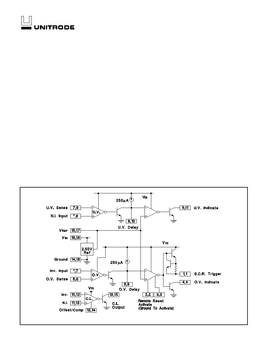
The monolithic integrated circuits contain all the functions necessary to monitor
and control the output of a sophisticated power supply system. Over-voltage (O.V.)
sensing with provision to trigger an external SCR "crowbar" shutdown; an under-
voltage (U.V.) circuit which can be used to monitor either the output or to sample
the input line voltage; and a third op amp/comparator usable for current sensing
(C.L.) are all included in this IC, together with an independent, accurate reference
generator.
Both over- and under-voltage sensing circuits can be externally programmed for
minimum time duration of fault before triggering. All functions contain open collec-
tor outputs which can be used independently or wire-or'ed together, and although
the SCR trigger is directly connected only to the over-voltage sensing circuit, it
may be optionally activated by any of the other outputs, or from an external signal.
The O.V. circuit also includes an optional latch and external reset capability.
The UC1544/2544/3544 devices have the added versatility of completely uncom-
mitted inputs to the voltage sensing comparators so that levels less than 2.5V may
be monitored by dividing down the internal reference voltage. The current sense
circuit may be used with external compensation as a linear amplifier or as a high-
gain comparator. Although nominally set for zero input offset, a fixed threshold may
be added with an external resistor. Instead of current limiting, this circuit may also
be used as an additional voltage monitor.
The reference generator circuit is internally trimmed to eliminate the need for ex-
ternal potentiometers and the entire circuit may be powered directly from either the
output being monitored or from a separate bias voltage.
BLOCK DIAGRAM
Note: For each terminal, first number refers to 1543 series, second to 1544 series.
* On 1543 series, this function is internally connected to V
REF.
UC1543 UC1544
UC2543 UC2544
UC3543 UC3544
DESCRIPTION
FEATURES
4/97

ABSOLUTE MAXIMUM RATINGS
Input Supply Voltage, V
IN
. . . . . . . . . . . . . . . . . . . . . . . . . . . . . . . . . . . . . . 40V
Sense Inputs, Voltage Range. . . . . . . . . . . . . . . . . . . . . . . . . . . . . . . . 0 to V
IN
SCR Trigger Current (Note 1) . . . . . . . . . . . . . . . . . . . . . . . . . . . . . . -600mA
Indicator Output Voltage . . . . . . . . . . . . . . . . . . . . . . . . . . . . . . . . . . . . . . . 40V
Indicator Output Sink Current . . . . . . . . . . . . . . . . . . . . . . . . . . . . . . . . . 50mA
Power Dissipation (Package Limitation). . . . . . . . . . . . . . . . . . . . . . . 1000mW
Operating Temperature Range
UC1543, UC1544 . . . . . . . . . . . . . . . . . . . . . . . . . . . . . . . . -55∞C to +125∞C
UC2543, UC2544 . . . . . . . . . . . . . . . . . . . . . . . . . . . . . . . . . -25∞C to +85∞C
UC3543, UC3544 . . . . . . . . . . . . . . . . . . . . . . . . . . . . . . . . . . 0∞C to +70∞C
Storage Temperature Range . . . . . . . . . . . . . . . . . . . . . . . . . -65∞C to +150∞C
Note 1: At higher input voltages, a dissipation limiting resistor, RG, is required.
Note 2: Currents are positive-into, negative-out of the specified terminal. Con-
sult Packaging section of Databook for thermal limitations and considerations
of package.
UC1543 UC1544
UC2543 UC2544
UC3543 UC3544
CONNECTION DIAGRAMS
DIL-16, SOIC-16 (TOP VIEW)
J or N, DW Package
UC 1543
UC 2543
UC 3543
DIL-18, SOIC-18 (TOP VIEW)
J or N, DW Package
UC 1544
UC 2544
UC 3544
PACKAGE PIN FUNCTION
FUNCTION
PIN
N/C
1
SCR Trigger
2
Remote Activate
3
Reset
4
O.V. Indicate
5
N/C
6
O.V. Delay
7
O.V. Input
8
N/C
9
N/C
10
U.V. Input
11
U.V. Delay
12
U.V. Indicate
13
C.L. INV. Input
14
C.L. N.I. Input
15
Offset/Comp
16
C.L. Output
17
Ground
18
V
REF
19
V
IN
20
PLCC-20, LCC-20
(TOP VIEW)
Q or L Package
PACKAGE PIN FUNCTION
FUNCTION
PIN
N/C
1
SCR Trigger
2
Remote Activate
3
Reset
4
O.V. Indicate
5
N/C
6
O.V. Delay
7
O.V. N.I. Input
8
O.V. INV. Input
9
U.V. N.I. Input
10
U.V. INV. Input
11
U.V. Delay
12
U.V. Indicate
13
C.L. INV. Input
14
C.L. N.I. Input
15
Offset/Comp
16
C.L. Output
17
Ground
18
V
REF
19
V
IN
20
PLCC-20, LCC-20
(TOP VIEW)
Q or L Package
2
PARAMETER
TEST CONDITIONS
UC1543/UC1544
UC2543/UC2544
UC3543/UC3544
UNITS
MIN
TYP
MAX
MIN
TYP
MAX
Input Voltage Range
T
J
= 25∞C to T
MAX
4.5
40
4.5
40
V
T
MIN
to T
MAX
4.7
40
4.7
40
V
Supply Current
V
IN
= 40V, Output Open, T
J
= 25∞C
7
10
7
10
mA
T
MIN
T
J
T
MAX
15
15
mA
Reference Section
Output Voltage
T
J
= 25∞C
2.48
2.50
2.52
2.45
2.50
2.55
V
Output Voltage
Over Temperature Range
2.45
2.55
2.40
2.60
V
Line Regulation
V
IN
= 5 to 30V
1
5
1
5
mV
Load Regulation
I
REF
= 0 to 10mA
1
10
1
10
mV
Short Circuit Current
V
REF
= 0
-10
-20
-40
-12
-20
-40
mA
Temperature Stability
50
50
ppm
/∞C
SCR Trigger Section
Peak Output Current
V
IN
= 5V, R
G
= 0, V
O
= 0
-100
-300
-600
-100
-300
-600
mA
Peak Output Voltage
V
IN
= 15V, I
O
= -100mA
12
13
12
13
V
Output Off Voltage
V
IN
= 40V
0
0.1
0
0.1
V
Remote Activate Current
R/A Pin = Gnd
-0.4
-0.8
-0.4
-0.8
mA
Remote Activate Voltage
R/A Pin Open
2
6
2
6
V
Reset Current
Reset = Gnd, R/A = Gnd
-0.4
-0.8
-0.4
-0.8
mA
Reset Voltage
Reset open, R/A = Gnd
2
6
2
6
V
Output Current Rise Time
R
L
= 50
, T
J
= 25∞C, C
D
= 0
400
400
mA/
µ
s
Prop. Delay from R/A
R
L
= 50
, T
J
= 25∞C, C
D
= 0
300
300
ns
Prop. Delay from O/V input R
L
= 50
, T
J
= 25∞C, C
D
= 0
500
500
ns
Comparator Section
Input Threshold (Input
voltage rising on O.V. and
falling on U.V.)
T
J
= 25∞C
2.45
2.50
2.55
2.40
2.50
2.60
V
Over Temperature Range
2.40
2.60
2.35
2.65
V
Input Hysteresis
25
25
mV
Input Bias Current
Sense Input = 0V
-0.3
-1.0
-0.3
-1.0
µ
A
Delay Saturation
0.2
0.5
0.2
0.5
V
Delay High Level
6
7
6
7
V
Delay Charging Current
V
O
= 0
-200
-250
-300
-200
-250
-300
µ
A
Indicate Saturation
I
L
= 10mA
0.2
0.5
0.2
0.5
V
Indicate Leakage
V
IND
= 40V
.01
1.0
.01
1.0
µ
A
Propagation Delay
Input Over Drive = 200mV, T
J
= 25∞C, C
D
= 0
400
400
ns
Input Over Drive = 200mV, T
J
= 25∞C, C
D
= 1
µ
F
10
10
ms
Current Limit Section
Input Voltage Range
0
V
IN
-3V
0
V
IN
-
3V
V
Input Bias Current
Offset Pin Open, V
CM
= 0
-0.3
-1.0
-0.3
-1.0
µ
A
Input Offset Voltage
Offset Pin Open, V
CM
= 0
0
10
0
10
mV
10k
from Offset Pin to Gnd
80
100
120
80
100
120
mV
CMRR
0
V
CM
12V, V
IN
= 15V
60
70
60
70
dB
AVOL
Offset Pin Open, V
CM
= 0V,
R
L
= 10k to 15k
,
V
OUT
= 1 to 6V
72
80
72
80
dB
Output Saturation
I
L
= 10mA
0.2
0.5
0.2
0.5
V
Output Leakage
V
IND
= 40V
.01
1.0
.01
1.0
µ
A
Small Signal Bandwidth
A
V
= 0dB, T
J
= 25∞C
5
5
MHz
Propagation Delay
V
OVERDRIVE
= 100mV, T
J
= 25∞C
200
200
ns
ELECTRICAL CHARACTERISTICS:
Unless otherwise stated, these specifications apply for T
A
= -55∞C to +125∞C for the
UC1543 and UC1544; -25∞C to +85∞C for the UC2543 and UC2544; and 0∞C to +70∞C for the UC3543 and UC3544. Electrical
tests are performed with V
IN
= 10V and 2k
pull-up resistors on all indicator outputs. All electrical specifications for the UC1544,
UC2544, and UC3544 devices are tested with the inverting over-voltage input and the non-inverting under-voltage input externally
connected to the 2.5V reference. T
A
= T
J.
UC1543 UC1544
UC2543 UC2544
UC3543 UC3544
3

UC1543 UC1544
UC2543 UC2544
UC3543 UC3544
Note: R
T
is connected from Offset Pin to Gnd. Values of
R
T
below 5.0k may cause Amplifier Cutoff at -55
∞
C.
SCR Trigger Power Limiting
Current Limit Amplifier Frequency Response
Activation Delay vs Capacitor Value
Comparator Input Hysteresis
Current Limit Input Threshold
Current Limit Amplifier Gain
4

UNITRODE CORPORATION
7 CONTINENTAL BLVD.
∑
MERRIMACK, NH 03054
TEL. (603) 424-2410
∑
FAX 603-424-3460
UC1543 UC1544
UC2543 UC2544
UC3543 UC3544
Overcurrent Shutdown
Input Line Monitor
APPLICATIONS (Pin numbers given for UC1543 series devices)
Typical Application
Sensing Multiple Supply Voltages
The values for the external components are determined
as follows:
Current limit input threshold, V
TH
=
1000
R
1
C
S
is determined by the current loop dynamics
Peak current to load, I
P
V
TH
R
SC
+
V
O
R
SC
R
2
R
2
+
R
3
Short Circuit Current, I
SC
=
V
TH
R
SC
Low output voltage limit, V
O
(Low) =
2.5
(
R
4
+
R
5
+
R
6
)
R
5
+
R
6
High output voltage limit, V
O
(High) =
2.5
(
R
4
+
R
5
+
R
6
)
R
6
Voltage sensing delay, t
D
= 10,000Cd
SCR trigger power limiting resistor, R
G
>
V
IN
-
5
0.2
5