1
Data sheet acquired from Harris Semiconductor
SCHS166F
Features
∑ Overriding RESET Terminates Output Pulse
∑ Triggering from the Leading or Trailing Edge
∑ Q and Q Buffered Outputs
∑ Separate Resets
∑ Wide Range of Output-Pulse Widths
∑ Schmitt Trigger on B Inputs
∑ Fanout (Over Temperature Range)
- Standard Outputs . . . . . . . . . . . . . . . 10 LSTTL Loads
- Bus Driver Outputs . . . . . . . . . . . . . 15 LSTTL Loads
∑ Wide Operating Temperature Range . . . -55
o
C to 125
o
C
∑ Balanced Propagation Delay and Transition Times
∑ Significant Power Reduction Compared to LSTTL
Logic ICs
∑ HC Types
- 2V to 6V Operation
- High Noise Immunity: N
IL
= 30%, N
IH
= 30% of V
CC
at V
CC
= 5V
∑ HCT Types
- 4.5V to 5.5V Operation
- Direct LSTTL Input Logic Compatibility,
V
IL
= 0.8V (Max), V
IH
= 2V (Min)
- CMOS Input Compatibility, I
l
1
µ
A at V
OL
, V
OH
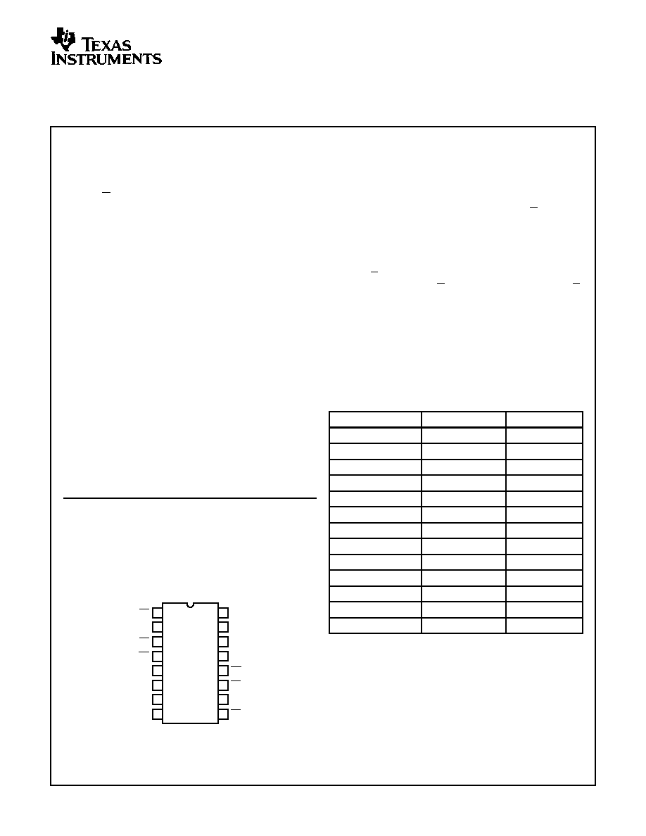
Pinout
CD54HC221
(CERDIP)
CD74HC221
(PDIP, SOIC, SOP, TSSOP)
CD74HCT221
(PDIP, SOIC)
TOP VIEW
Description
The 'HC221 and CD74HCT221 are dual monostable
multivibrators with reset. An external resistor (R
X
) and an
external capacitor (C
X
) control the timing and the accuracy
for the circuit. Adjustment of R
X
and C
X
provides a wide
range of output pulse widths from the Q and Q terminals.
Pulse triggering on the B input occurs at a particular voltage
level and is not related to the rise and fall time of the trigger
pulse.
Once triggered, the outputs are independent of further trigger
inputs on A and B. The output pulse can be terminated by a
LOW level on the Reset (R) pin. Trailing Edge triggering (A)
and leading-edge-triggering (B) inputs are provided for
triggering from either edge of the input pulse. On power up,
the IC is reset. If either Mono is not used each input (on the
unused device) must be terminated either high or low.
The minimum value of external resistance, R
X
, is typically 500
.
The minimum value of external capacitance, C
X
, is 0pF. The
calculation for the pulse width is t
W
= 0.7 R
X
C
X
at V
CC
= 4.5V.
14
15
16
9
13
12
11
10
1
2
3
4
5
7
6
8
1A
1B
1R
1Q
2Q
2C
X
GND
2C
X
R
X
V
CC
1C
X
1Q
2Q
2R
2B
2A
1C
X
R
X
Ordering Information
PART NUMBER
TEMP. RANGE (
o
C)
PACKAGE
CD54HC221F3A
-55 to 125
16 Ld CERDIP
CD74HC221E
-55 to 125
16 Ld PDIP
CD74HC221M
-55 to 125
16 Ld SOIC
CD74HC221MT
-55 to 125
16 Ld SOIC
CD74HC221M96
-55 to 125
16 Ld SOIC
CD74HC221NSR
-55 to 125
16 Ld SOP
CD74HC221PW
-55 to 125
16 Ld TSSOP
CD74HC221PWR
-55 to 125
16 Ld TSSOP
CD74HC221PWT
-55 to 125
16 Ld TSSOP
CD74HCT221E
-55 to 125
16 Ld PDIP
CD74HCT221M
-55 to 125
16 Ld SOIC
CD74HCT221MT
-55 to 125
16 Ld SOIC
CD74HCT221M96
-55 to 125
16 Ld SOIC
NOTE: When ordering, use the entire part number. The suffixes 96
and R denote tape and reel. The suffix T denotes a small-quantity
reel of 250.
November 1997 - Revised October 2003
CAUTION: These devices are sensitive to electrostatic discharge. Users should follow proper IC Handling Procedures.
Copyright
©
2003, Texas Instruments Incorporated
CD54HC221, CD74HC221,
CD74HCT221
High-Speed CMOS Logic
Dual Monostable Multivibrator with Reset
[ /Title
(CD74
HC221
,
CD74
HCT22
1)
/Sub-
ject
(High
Speed
CMOS
Logic
Dual
Monos
table
Multi-
2
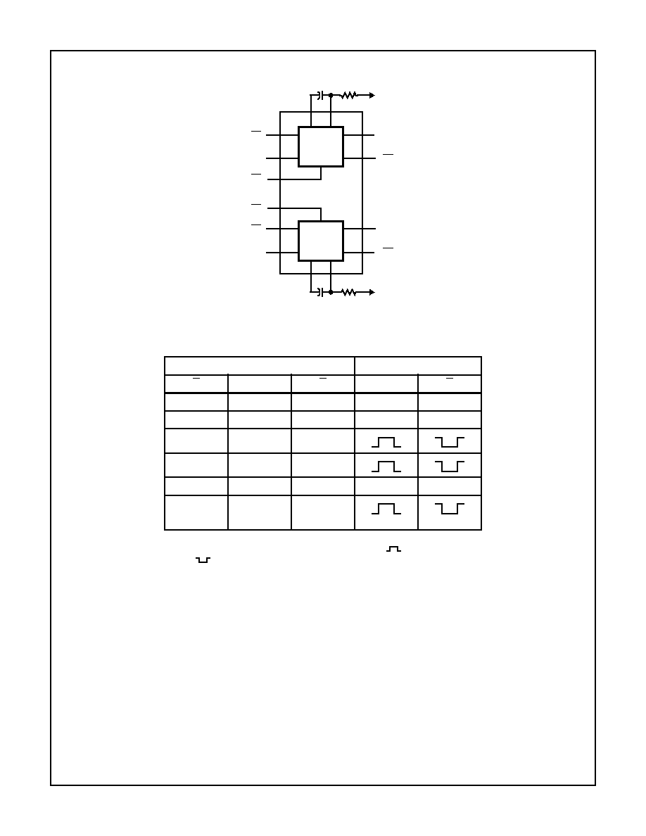
Functional Diagram
TRUTH TABLE
INPUTS
OUTPUTS
A
B
R
Q
Q
H
X
H
L
H
X
L
H
L
H
L
H
H
H
X
X
L
L
H
L
H
(Note 3)
(Note 3)
H = High Voltage Level, L = Low Voltage Level, X = Irrelevant,
= Transition from
Low to High Level,
= Transition from High to Low Level,
= One High Level
Pulse,
= One Low Level Pulse
NOTE:
1. For this combination the reset input must be low and the following sequence
must be used: pin 1 (or 9) must be set high or pin 2 (or 10) set low; then pin 1
(or 9) must be low and pin 2 (or 10) set high. Now the reset input goes from low-
to-high and the device will be triggered.
2R
11
2A
9
10
5
12
2Q
2Q
2B
MONO 2
V
CC
6
7
2C
X
2C
X
R
X
1R
3
1A
2
1
13
4
1Q
1Q
1B
MONO 1
V
CC
14
15
1C
X
1C
X
R
X
1C
X
1R
X
2C
X
2R
X
CD54HC221, CD74HC221, CD74HCT221
3
Logic Diagram
1 (9)
A
2 (10)
B
S
QM
QM
R
S
MASK
FF
MAIN
FF
Q
Q
R
3 (11)
4 (12)
(13) 5
Q
Q
C
P
Q
R
Q
D
C
C
V
CC
R
D
C
Q
C
RESET
FF
V
CC
P P
R1
PULLDOWN
FF
N
-
+
MIRROR VOLTAGE
V
CC
+
-
P
OP
AMP
R3
P
R2
R4
N
GND
8
15 (7)
R
X
C
X
V
CC
16
C
X
C
X
14 (6)
OP AMP
R
R
X
N
CD54HC221, CD74HC221, CD74HCT221
4
Absolute Maximum Ratings
Thermal Information
DC Supply Voltage, V
CC
. . . . . . . . . . . . . . . . . . . . . . . . -0.5V to 7V
DC Input Diode Current, I
IK
For V
I
< -0.5V or V
I
> V
CC
+ 0.5V
. . . . . . . . . . . . . . . . . . . . . .±
20mA
DC Output Diode Current, I
OK
For V
O
< -0.5V or V
O
> V
CC
+ 0.5V
. . . . . . . . . . . . . . . . . . . .±
20mA
DC Drain Current, per Output, I
O
For -0.5V < V
O
< V
CC
+ 0.5V
. . . . . . . . . . . . . . . . . . . . . . . . . .±
25mA
DC Output Source or Sink Current per Output Pin, I
O
For V
O
> -0.5V or V
O
< V
CC
+ 0.5V
. . . . . . . . . . . . . . . . . . . .±
25mA
DC V
CC
or Ground Current, I
CC
. . . . . . . . . . . . . . . . . . . . . . . . .±
50mA
Operating Conditions
Temperature Range, T
A
. . . . . . . . . . . . . . . . . . . . . . -55
o
C to 125
o
C
Supply Voltage Range, V
CC
HC Types . . . . . . . . . . . . . . . . . . . . . . . . . . . . . . . . . . . . .2V to 6V
HCT Types . . . . . . . . . . . . . . . . . . . . . . . . . . . . . . . . .4.5V to 5.5V
DC Input or Output Voltage, V
I
, V
O
. . . . . . . . . . . . . . . . . 0V to V
CC
Input Rise and Fall Time, t
r
, t
f
on Inputs A and R
2V . . . . . . . . . . . . . . . . . . . . . . . . . . . . . . . . . . . . . . 1000ns (Max)
4.5V. . . . . . . . . . . . . . . . . . . . . . . . . . . . . . . . . . . . . . 500ns (Max)
6V . . . . . . . . . . . . . . . . . . . . . . . . . . . . . . . . . . . . . . . 400ns (Max)
Input Rise and Fall Time, t
r
, t
f
on Input B
2V . . . . . . . . . . . . . . . . . . . . . . . . . . . . . . . . . . Unlimited ns (Max)
4.5V. . . . . . . . . . . . . . . . . . . . . . . . . . . . . . . . . Unlimited ns (Max)
6V . . . . . . . . . . . . . . . . . . . . . . . . . . . . . . . . . . Unlimited ns (Max)
Package Thermal Impedance,
JA
(see Note 2):
E (PDIP) Package . . . . . . . . . . . . . . . . . . . . . . . . . . . . . . . 67
o
C/W
M (SOIC) Package. . . . . . . . . . . . . . . . . . . . . . . . . . . . . . . 73
o
C/W
NS (SOP) Package . . . . . . . . . . . . . . . . . . . . . . . . . . . . . . 64
o
C/W
PW (TSSOP) Package . . . . . . . . . . . . . . . . . . . . . . . . . 108
o
C/W
Maximum Junction Temperature (Plastic Package) . . . . . . . . 150
o
C
Maximum Storage Temperature Range . . . . . . . . . .-65
o
C to 150
o
C
Maximum Lead Temperature (Soldering 10s) . . . . . . . . . . . . . 300
o
C
(SOIC - Lead Tips Only)
CAUTION: Stresses above those listed in "Absolute Maximum Ratings" may cause permanent damage to the device. This is a stress only rating and operation
of the device at these or any other conditions above those indicated in the operational sections of this specification is not implied.
NOTE:
2. The package thermal impedance is calculated in accordance with JESD 51-7.
DC Electrical Specifications
PARAMETER
SYMBOL
TEST
CONDITIONS
V
CC
(V)
25
o
C
-40
o
C TO 85
o
C -55
o
C TO 125
o
C
UNITS
V
I
(V)
I
O
(mA)
MIN
TYP
MAX
MIN
MAX
MIN
MAX
HC TYPES
High Level Input
Voltage
V
IH
-
-
2
1.5
-
-
1.5
-
1.5
-
V
4.5
3.15
-
-
3.15
-
3.15
-
V
6
4.2
-
-
4.2
-
4.2
-
V
Low Level Input
Voltage
V
IL
-
-
2
-
-
0.5
-
0.5
-
0.5
V
4.5
-
-
1.35
-
1.35
-
1.35
V
6
-
-
1.8
-
1.8
-
1.8
V
High Level Output
Voltage
CMOS Loads
V
OH
V
IH
or V
IL
-0.02
2
1.9
-
-
1.9
-
1.9
-
V
-0.02
4.5
4.4
-
-
4.4
-
4.4
-
V
-0.02
6
5.9
-
-
5.9
-
5.9
-
V
High Level Output
Voltage
TTL Loads
-
-
-
-
-
-
-
-
-
V
-4
4.5
3.98
-
-
3.84
-
3.7
-
V
-5.2
6
5.48
-
-
5.34
-
5.2
-
V
Low Level Output
Voltage
CMOS Loads
V
OL
V
IH
or V
IL
0.02
2
-
-
0.1
-
0.1
-
0.1
V
0.02
4.5
-
-
0.1
-
0.1
-
0.1
V
0.02
6
-
-
0.1
-
0.1
-
0.1
V
Low Level Output
Voltage
TTL Loads
-
-
-
-
-
-
-
-
-
V
4
4.5
-
-
0.26
-
0.33
-
0.4
V
5.2
6
-
-
0.26
-
0.33
-
0.4
V
CD54HC221, CD74HC221, CD74HCT221

5
Input Leakage
Current
I
I
V
CC
or
GND
-
6
-
-
±
0.1
-
±
1
-
±
1
µ
A
Quiescent Device
Current
I
CC
V
CC
or
GND
0
6
-
-
8
-
80
-
160
µ
A
HCT TYPES
High Level Input
Voltage
V
IH
-
-
4.5 to
5.5
2
-
-
2
-
2
-
V
Low Level Input
Voltage
V
IL
-
-
4.5 to
5.5
-
-
0.8
-
0.8
-
0.8
V
High Level Output
Voltage
CMOS Loads
V
OH
V
IH
or V
IL
-0.02
4.5
4.4
-
-
4.4
-
4.4
-
V
High Level Output
Voltage
TTL Loads
-4
4.5
3.98
-
-
3.84
-
3.7
-
V
Low Level Output
Voltage
CMOS Loads
V
OL
V
IH
or V
IL
0.02
4.5
-
-
0.1
-
0.1
-
0.1
V
Low Level Output
Voltage
TTL Loads
4
4.5
-
-
0.26
-
0.33
-
0.4
V
Input Leakage
Current
I
I
V
CC
and
GND
0
5.5
-
±
0.1
-
±
1
-
±
1
µ
A
Quiescent Device
Current
I
CC
V
CC
or
GND
0
5.5
-
-
8
-
80
-
160
µ
A
Additional Quiescent
Device Current Per
Input Pin: 1 Unit Load
I
CC
(Note 3)
V
CC
-2.1
-
4.5 to
5.5
-
100
360
-
450
-
490
µ
A
NOTE:
3. For dual-supply systems theoretical worst case (V
I
= 2.4V, V
CC
= 5.5V) specification is 1.8mA.
DC Electrical Specifications
(Continued)
PARAMETER
SYMBOL
TEST
CONDITIONS
V
CC
(V)
25
o
C
-40
o
C TO 85
o
C -55
o
C TO 125
o
C
UNITS
V
I
(V)
I
O
(mA)
MIN
TYP
MAX
MIN
MAX
MIN
MAX
HCT Input Loading Table
INPUT
UNIT LOADS
All Inputs
0.3
NOTE: Unit Load is
I
CC
limit specified in DC Electrical Table, e.g.,
360
µ
A max at 25
o
C.
Prerequisite For Switching Function
PARAMETER
SYMBOL
V
CC
(V)
25
o
C
-40
o
C TO 85
o
C
-55
o
C TO 125
o
C
UNITS
MIN
TYP
MAX
MIN
MAX
MIN
MAX
HC TYPES
Input Pulse Width
A
t
WL
2
70
-
-
90
-
105
-
ns
4.5
14
-
-
18
-
21
-
ns
6
12
-
-
15
-
18
-
ns
Input Pulse Width
B
t
WH
2
70
-
-
90
-
105
-
ns
4.5
14
-
-
18
-
21
-
ns
6
12
-
-
15
-
18
-
ns
CD54HC221, CD74HC221, CD74HCT221