SMJ320C25, SMJ320C25 50
DIGITAL SIGNAL PROCESSOR
SGUS007D ≠ AUGUST 1988 ≠ REVISED OCTOBER 2001
1
POST OFFICE BOX 1443
∑
HOUSTON, TEXAS 77251≠1443
D
Military Temperature Range
≠ ≠55
∞
C to 125
∞
C
D
100-ns or 80-ns Instruction Cycle Times
D
544 Words of Programmable On-Chip Data
RAM
D
4K Words of On-Chip Program ROM
D
128K Words of Data/Program Space
D
16 Input and 16 Output Channels
D
16-Bit Parallel Interface
D
Directly Accessible External Data Memory
Space
≠ Global Data Memory Interface
D
16-Bit Instruction and Data Words
D
16
◊
16-Bit Multiplier With a 32-Bit Product
D
32-Bit ALU and Accumulator
D
Single-Cycle Multiply/Accumulate
Instructions
D
0 to 16-Bit Scaling Shifter
D
Bit Manipulation and Logical Instructions
D
Instruction Set Support for Floating-Point
Operations, Adaptive Filtering, and
Extended-Precision Arithmetic
D
Block Moves for Data/Program
Management
D
Repeat Instructions for Efficient Use of
Program Space
D
Eight Auxiliary Registers and Dedicated
Arithmetic Unit for Indirect Addressing
D
Serial Port for Direct Code Interface
D
Synchronization Input for Synchronous
Multiprocessor Configurations
D
Wait States for Communication to
Slow-Off-Chip Memories/Peripherals
D
On-Chip Timer for Control Operations
D
Three External Maskable User Interrupts
D
Input Pin Polled by Software Branch
Instruction
D
1.6-
µ
m CMOS Technology
D
Programmable Output Pin for Signaling
External Devices
D
Single 5-V Supply
D
On-Chip Clock Generator
D
Packaging:
≠ 68-Pin Leaded Ceramic Chip Carrier (FJ
Suffix)
≠ 68-Pin Ceramic Grid Array (GB Suffix)
≠ 68-Pin Leadless Ceramic Chip Carrier
(FD Suffix)
Copyright
2001, Texas Instruments Incorporated
PRODUCTION DATA information is current as of publication date.
Products conform to specifications per the terms of Texas Instruments
standard warranty. Production processing does not necessarily include
testing of all parameters.
Please be aware that an important notice concerning availability, standard warranty, and use in critical applications of
Texas Instruments semiconductor products and disclaimers thereto appears at the end of this data sheet.
IACK
MSC
CLKOUT1
CLKOUT2
XF
HOLDA
DX
FSX
X2 CLKIN
X1
BR
D8
D9
D10
D1
1
D12
D13
D14
D15
READY
CLKR
CLKX
STRB
R/W
PS
IS
DS
VSS
10
11
12
13
14
15
16
17
18
19
20
21
22
23
24
25
26
27 28 29 30 31 32 33 34 35 36 37 38 39 40 41 42 43
9 8 7 6 5 4 3 2 1 68 67 66 65 64 63 62 61
VSS
D7
D6
D5
D4
D3
D2
D1
D0
SYNC
INT0
INT1
INT2
VCC
DR
FSR
A0
60
59
58
57
56
55
54
53
52
51
50
49
48
47
46
45
44
A1
A2
A3
A4
A5
A6
A7
A8
A9
A10
A1
1
A12
A13
A14
A15
V
SS
V
CC
V
CC
V
CC
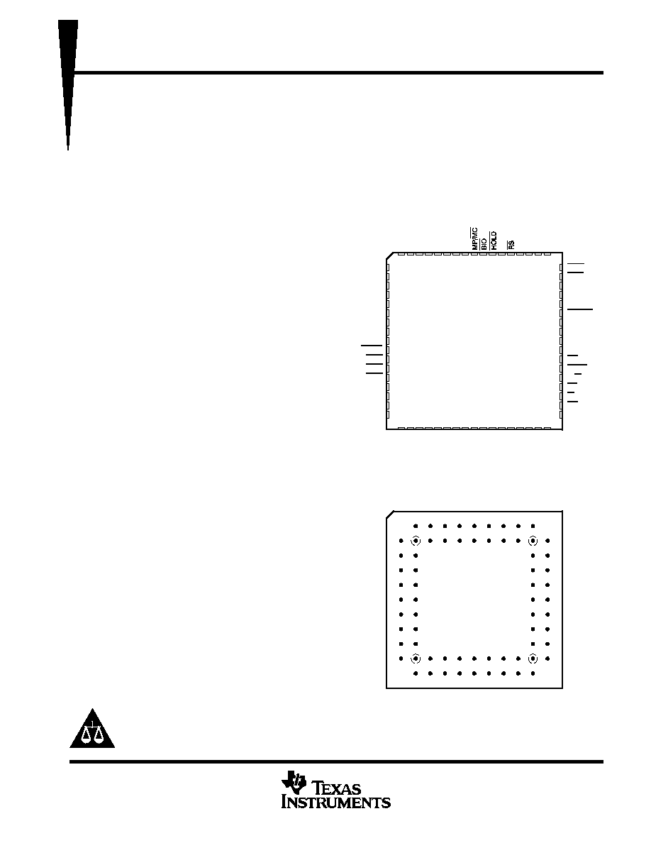
68-Pin FJ and FD Packages
(Top View)
On products compliant to MIL PRF 38535, all parameters are tested
unless otherwise noted. On all other products, production
processing does not necessarily include testing of all parameters.
1
2
3
4
5
6
7
8
9 10 11
A
B
C
D
E
F
G
H
J
K
L
68-Pin GB Package
(Top View)
SMJ320C25, SMJ320C25 50
DIGITAL SIGNAL PROCESSOR
SGUS007D ≠ AUGUST 1988 ≠ REVISED OCTOBER 2001
2
POST OFFICE BOX 1443
∑
HOUSTON, TEXAS 77251≠1443
description
This data sheet provides design documentation for the SMJ320C25 and the SMJ320C25-50 digital signal
processor (DSP) devices in the SMJ320
family of VLSI digital signal processors and peripherals. The SMJ320
family supports a wide range of digital signal processing applications such as tactical communications,
guidance, military modems, speech processing, spectrum analysis, audio processing, digital filtering,
high-speed control, graphics, and other computation-intensive applications.
Differences between the SMJ320C25 and the SMJ320C25-50 are specifically identified, as in the following
paragraph and in the parameter tables on pages 18 through 24 of this data sheet. When not specifically
differentiated, the term SMJ320C25 is used to describe both devices.
The SMJ320C25 has a 100-ns instruction cycle time. The SMJ320C25-50 has an 80-ns instruction cycle time.
With these fast instruction cycle times and their innovative memory configurations, these devices perform
operations necessary for many real-time digital signal processing algorithms. Since most instructions require
only one cycle, the SMJ320C25 is capable of executing 12.5 million instructions per second. On-chip data RAM
of 544 16-bit words, on-chip program ROM of 4K words, direct addressing of up to 64K words of external data
memory space and 64K words of external program memory space, and multiprocessor interface features for
sharing global memory minimize unnecessary data transfers to take full advantage of the capabilities of the
instruction set.
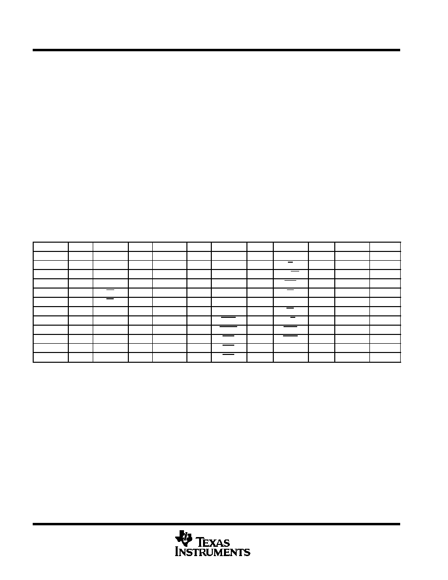
Table 1. PGA/CLCC/LCCC Pin Assignments
FUNCTION
PIN
FUNCTION
PIN
FUNCTION
PIN
FUNCTION
PIN
FUNCTION
PIN
FUNCTION
PIN
A0
K1/26
A12
K8/40
D2
E1/16
D14
A5/3
INT2
H1/22
VCC
H2/23
A1
K2/28
A13
L9/41
D3
D2/15
D15
B6/2
IS
J11/46
VCC
L6/35
A2
L3/29
A14
K9/42
D4
D1/14
DR
J1/24
MP/MC
A6/1
VSS
B1/10
A3
K3/30
A15
L10/43
D5
C2/13
DS
K10/45
MSC
C10/59
VSS
K11/44
A4
L4/31
BI0
B7/68
D6
C1/12
DX
E11/54
PS
J10/47
VSS
L2/27
A5
K4/32
BR
G11/50
D7
B2/11
FSR
J2/25
READY
B8/66
XF
D11/56
A6
L5/33
CLKOUT1
C11/58
D8
A2/9
FSX
F10/53
RS
A8/65
X1
G10/51
A7
K5/34
CLKOUT2
D10/57
D9
B3/8
HOLD
A7/67
R/W
H11/48
X2/CLKIN
F11/52
A8
K6/36
CLKR
B9/64
D10
A3/7
HOLDA
E10/55
STRB
H10/49
A9
L7/37
CLKX
A9/63
D11
B4/6
IACK
B11/60
SYNC
F2/19
A10
K7/38
D0
F1/18
D12
A4/5
INT0
G1/20
VCC
A10/61
A11
L8/39
D1
E2/17
D13
85/4
INT1
G2/21
VCC
B10/62
SMJ320 is a trademark of Texas Instruments Incorporated.
SMJ320C25, SMJ320C25 50
DIGITAL SIGNAL PROCESSOR
SGUS007D ≠ AUGUST 1988 ≠ REVISED OCTOBER 2001
3
POST OFFICE BOX 1443
∑
HOUSTON, TEXAS 77251≠1443
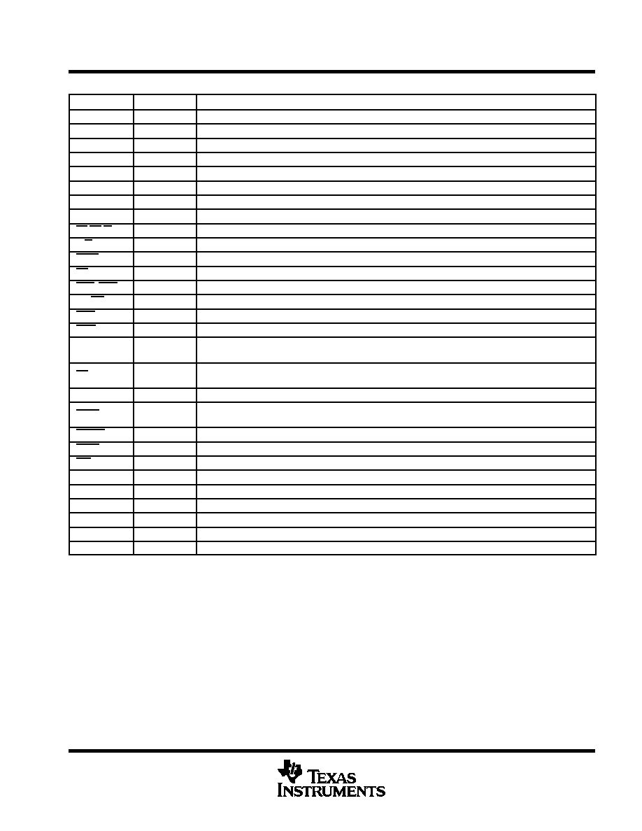
Terminal Functions
SIGNALS
I/O/Z
DEFINITION
VCC
I
5-V supply pins
VSS
I
Ground pins
X1
0
Output from internal oscillator for crystal
X2/CLKIN
I
Input to internal oscillator from crystal or external clock
CLKOUT1
0
Master clock output (crystal or CLKIN frequency/4)
CLKOUT2
0
A second clock output signal
D15≠D0
I/O/Z
16-bit data bus D15 (MSB) through D0 (LSB). Multiplexed between program, data, and I/0 spaces.
A15≠A0
O/Z
16-bit address bus A15 (MSB) through A0 (LSB)
PS,DS,IS
O/Z
Program, data, and I/O space select signals
R/W
O/Z
Read / write signal
STRB
O/Z
Strobe signal
RS
I
Reset input
INT2≠INT0
I
External user interrupt inputs
MP/MC
I
Microprocessor/microcomputer mode select pin
MSC
0
Microstate complete signal
IACK
0
Interrupt acknowledge signal
READY
I
Data ready input. Asserted by external logic when using slower devices to indicate that the current bus
transaction is complete.
BR
0
Bus request signal. Asserted when the SMJ320C25 requires access to an external global data memory
space.
XF
0
External flag output (latched software-programmable signal)
HOLD
1
Hold input. When asserted, SMJ320C25 goes into an idle mode and places the data, address, and
control lines in the high-impedance state.
HOLDA
0
Hold acknowledge signal
SYNC
I
Synchronization input
BIO
I
Branch control input. Polled by BIOZ instruction
DR
I
Serial data receive input
CLKR
I
Clock for receive input for serial port
FSR
I
Frame synchronization pulse for receive input
DX
O/Z
Serial data transmit output
CLKX
I
Clock for transmit output for serial port
FSX
I/O/Z
Frame synchronization pulse for transmit. Configurable as either an input or an output.
I/O/Z denotes input/output/high-impedance state.
SMJ320C25, SMJ320C25 50
DIGITAL SIGNAL PROCESSOR
SGUS007D ≠ AUGUST 1988 ≠ REVISED OCTOBER 2001
4
POST OFFICE BOX 1443
∑
HOUSTON, TEXAS 77251≠1443
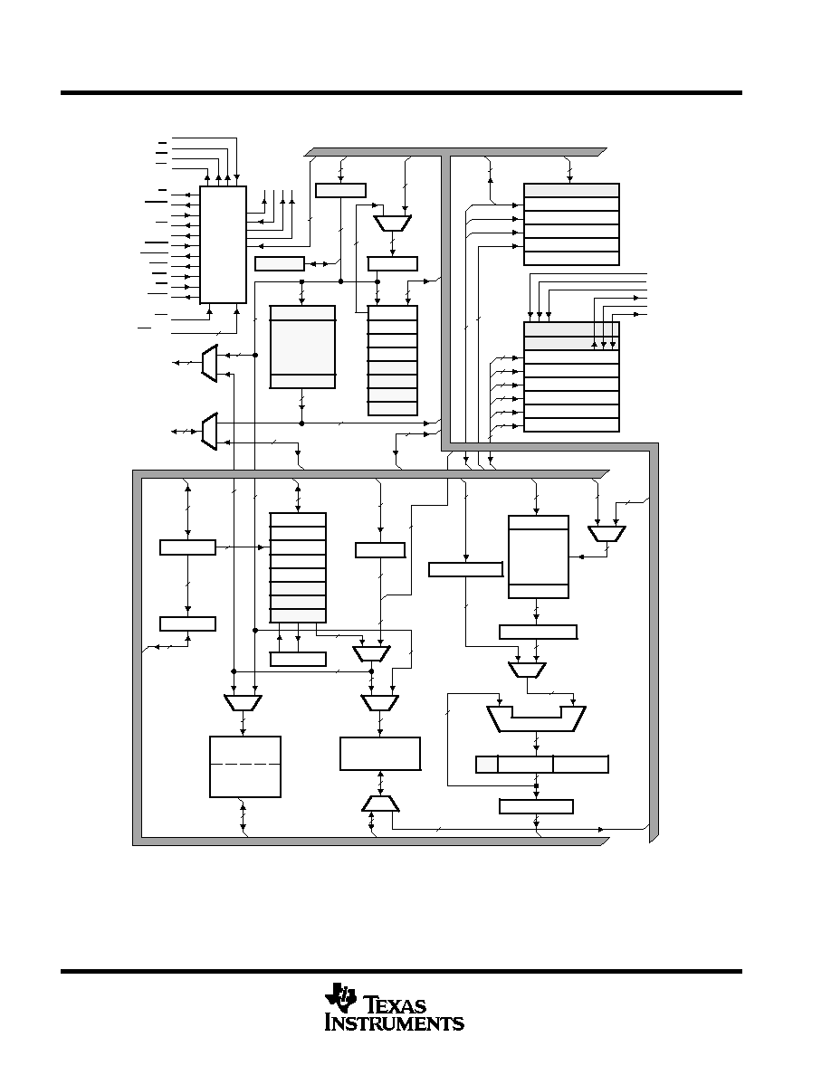
block diagram
Data Bus
Data Bus
16
16
16
16
16
16
Shifters (0-7)
ACCL(16)
32
ACCH(16)
32
32
ALU(32)
32
32
32
Shifter(-6, 0, 1, 4)
16
Shifter(0-16)
7 LSB
From IR
9
9
16
16
16
32
TR(16)
16
Multiplier
PR(32)
DATA/PROG
RAM (256
◊
16)
Block B0
16
16
16
16
16
Data RAM
Block B1
(256
◊
16)
Block B2
(32
◊
16)
3
ARB(3)
3
3
3
ARP(3)
ARAU(16)
AR4(16)
AR3(16)
AR2(16)
AR1(16)
16
AR0(16)
DP(9)
16
FSX
CLKX
DX
FSR
CLKR
DRR(16)
DXR(16)
PRD(16)
TIM(16)
IMR(6)
GREG(8)
16
16
IFR(6)
RPTC(8)
STO(16)
ST1(16)
IR(16)
3
16
16
16
16
16
D15-D0
16
16
16
16
A15-A0
INT(2-0)
MP/MC
Instruction
(8 x 16)
16
16
16
16
16
16
16
16
16
Stack
PC(16)
16
IACK
RS
BIO
MSC
HOLDA
HOLD
XF
BR
STRB
R/W
Program Bus
Program Bus
Program
ROM/
EPROM
(4096
◊
16)
QIR(16)
16
16
16
6
8
16
16
16
X1
X2/CLKIN
CLKOUT1
CLKOUT2
Controller
16
PFC(16)
MCS(16)
PS
DS
IS
SYNC
MUX
MUX
MUX
MUX
MUX
MUX
MUX
DR
MUX
MUX
C
READY
Address
AR5(16)
AR6(16)
AR7(16)
RSR(16)
XSR(16)
LEGEND:
ACCH
=
Accumulator high
IFR
=
Interrupt flag register
PC
= Program counter
ACCL
=
Accumulator low
IMR
=
Interrupt mask register
PFC
= Prefetch counter
ALU
=
Arithmetic logic unit
IR
=
Instruction register
RPTC
= Repeat instruction counter
ARAU
=
Auxiliary register arithmetic unit
MCS
=
Microcall stack
GREG
= Global memory allocation register
ARB
=
Auxiliary register pointer buffer
QIR
=
Queue instruction register
RSR
= Serial port receive shift register
ARP
=
Auxiliary register pointer
PR
=
Product register
XSR
= Serial port transmit shift register
DP
=
Data memory page pointer
PRD
=
Period register for timer
AR0-AR7
= Auxiliary registers
DRR
=
Serial port data receive register
TIM
=
Timer
ST0, ST1
= Status registers
DXR
=
Serial port data transmit register
TR
=
Temporary register
C
= Carry bit

SMJ320C25, SMJ320C25 50
DIGITAL SIGNAL PROCESSOR
SGUS007D ≠ AUGUST 1988 ≠ REVISED OCTOBER 2001
5
POST OFFICE BOX 1443
∑
HOUSTON, TEXAS 77251≠1443
architecture
The SMJ320C25 increases performance of DSP algorithms through innovative additions to the SMJ320
architecture. Increased throughput on the SMJ320C25 for many DSP applications is accomplished by means
of single-cycle multiply/accumulate instructions with a data move option, eight auxiliary registers with a
dedicated arithmetic unit, and faster I/O necessary for data-intensive signal processing.
The architectural design of the SMJ320C25 emphasizes overall speed, communication, and flexibility in
processor configuration. Control signals and instructions provide floating-point support, block-memory
transfers, communication to slower off-chip devices, and multiprocessing implementations.
Two large on-chip RAM blocks, configurable either as separate program and data spaces or as two contiguous
data blocks, provide increased flexibility in system design. Programs of up to 4K words can be masked into the
internal program ROM. The remainder of the 64K-word program memory space is located externally. Large
programs can execute at full speed from this memory space. Programs can also be downloaded from slow
external memory to high-speed on-chip RAM. A total of 64K data memory address space is included to facilitate
implementation of DSP algorithms. The VLSI implementation of the SMJ320C25 incorporates all of these
features as well as many others, such as a hardware timer, serial port, and block data transfer capabilities.
32-bit ALU/accumulator
The SMJ320C25 32-bit arithmetic logic unit (ALU) and accumulator perform a wide range of arithmetic and
logical instructions, the majority of which execute in a single clock cycle. The ALU executes a variety of branch
instructions dependent on the status of the ALU or a single bit in a word. These instruction provide the following
capabilities:
D
Branch to an address specified by the accumulator
D
Normalize fixed-point numbers contained in the accumulator
D
Test a specified bit of a word in data memory.
One input to the ALU is always provided from the accumulator, and the other input can be provided from the
product register (PA) of the multiplier or the input scaling shifter which has fetched data from the RAM on the
data bus. After the ALU has performed the arithmetic or logical operations, the result is stored in the
accumulator.
The 32-bit accumulator is split into two 16-bit segments for storage in data memory. Additional shifters at the
output of the accumulator perform shifts while the data is being transferred to the data bus for storage. The
contents of the accumulator remain unchanged.
scaling shifter
The SMJ320C25 scaling shifter has a 16-bit input connected to the data bus and a 32-bit output connected to
the ALU. The scaling shifter produces a left shift of 0 to 16 bits on the input data, as programmed in the
instruction. The LSBs of the output are filled with zeroes, and the MSBs can be either filled with zeroes or
sign-extended, depending upon the status programmed into the SXM (sign-extension mode) bit of status
register ST1.
16 X 16-bit parallel multiplier
The SMJ320C25 has a 16 x 16-bit hardware multiplier, which is capable of computing a signed or unsigned
32-bit product in a single machine cycle. The multiplier has the following two associated registers:
D
A 16-bit temporary register (TR) that holds one of the operands for the multiplier, and
D
A 32-bit product register (PR) that holds the product.
Incorporated into the SMJ320C25 instruction set are single-cycle multiply/accumulate instruction that allow
both operands to be processed simultaneously. The data for these operations can reside anywhere in internal
or external memory and can be transferred to the multiplier each cycle via the program and data buses.