SN54HC253, SN74HC253
DUAL 4 LINE TO 1 LINE DATA SELECTORS/MULTIPLEXERS
WITH 3 STATE OUTPUTS
SCLS133E - DECEMBER 1982 - REVISED SEPTEMBER 2003
1
POST OFFICE BOX 655303
∑
DALLAS, TEXAS 75265
D
3-State Version of 'HC153
D
Wide Operating Voltage Range of 2 V to 6 V
D
High-Current Inverting Outputs Drive Up To
15 LSTTL Loads
D
Low Power Consumption, 80-
µ
A Max I
CC
D
Typical t
pd
= 9 ns
D
±
6-mA Output Drive at 5 V
D
Low Input Current of 1
µ
A Max
D
Permit Multiplexing From n Lines to One
Line
D
Perform Parallel-to-Serial Conversion
description/ordering information
Each of these data selectors/multiplexers
contains inverters and drivers to supply full binary
decoding data selection to the AND-OR gates.
Separate output-control inputs are provided for
each of the two 4-line sections.
The 3-state outputs can interface with and drive
data lines of bus-organized systems. With all but
one of the common outputs disabled (in the
high-impedance state), the low impedance of the
single enabled output drives the bus line to a high
or low logic level. Each output has its own
output-enable (OE) input. The outputs are
disabled when their respective OE is high.
ORDERING INFORMATION
TA
PACKAGE
ORDERABLE
PART NUMBER
TOP-SIDE
MARKING
PDIP - N
Tube of 25
SN74HC253N
SN74HC253N
Tube of 40
SN74HC253D
-40
∞
C to 85
∞
C
SOIC - D
Reel of 2500
SN74HC253DR
HC253
-40
∞
C to 85
∞
C
SOIC - D
Reel of 250
SN74HC253DT
HC253
SOP - NS
Reel of 2000
SN74HC253NSR
HC253
SSOP - DB
Reel of 2000
SN74HC253DBR
HC253
CDIP - J
Tube of 25
SNJ54HC253J
SNJ54HC253J
-55
∞
C to 125
∞
C
CFP - W
Tube of 150
SNJ54HC253W
SNJ54HC253W
-55 C to 125 C
LCCC - FK
Tube of 55
SNJ54HC253FK
SNJ54HC253FK
Package drawings, standard packing quantities, thermal data, symbolization, and PCB design guidelines are
available at www.ti.com/sc/package.
Please be aware that an important notice concerning availability, standard warranty, and use in critical applications of
Texas Instruments semiconductor products and disclaimers thereto appears at the end of this data sheet.
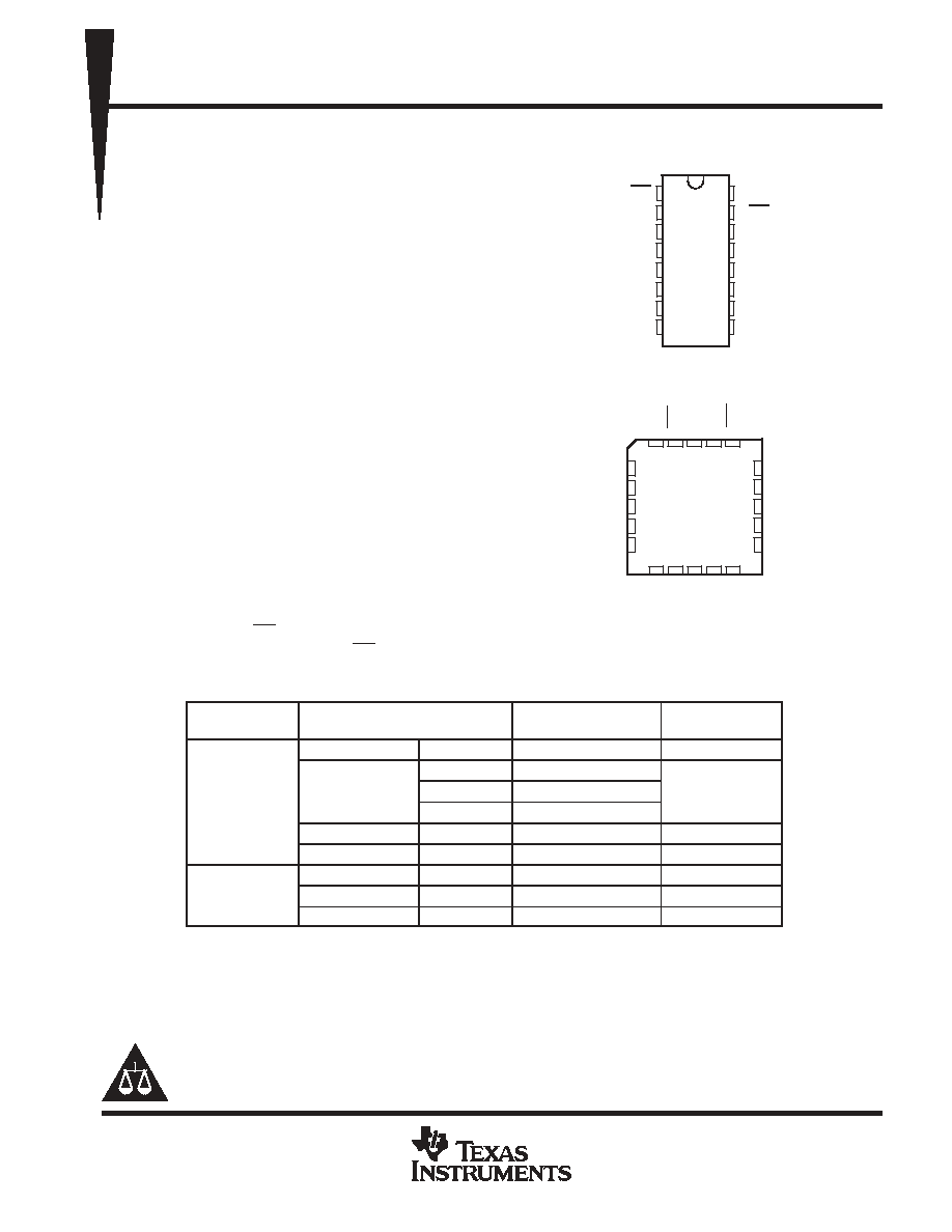
SN54HC253 . . . J OR W PACKAGE
SN74HC253 . . . D, DB, N, OR NS PACKAGE
(TOP VIEW)
3
2 1 20 19
9 10 11 12 13
4
5
6
7
8
18
17
16
15
14
A
2C3
NC
2C2
2C1
1C3
1C2
NC
1C1
1C0
SN54HC253 . . . FK PACKAGE
(TOP VIEW)
B
1OE
NC
2Y
2C0
2OE
1Y
GND
NC
V
CC
1
2
3
4
5
6
7
8
16
15
14
13
12
11
10
9
1OE
B
1C3
1C2
1C1
1C0
1Y
GND
V
CC
2OE
A
2C3
2C2
2C1
2C0
2Y
NC - No internal connection
Copyright
2003, Texas Instruments Incorporated
PRODUCTION DATA information is current as of publication date.
Products conform to specifications per the terms of Texas Instruments
standard warranty. Production processing does not necessarily include
testing of all parameters.
On products compliant to MIL PRF 38535, all parameters are tested
unless otherwise noted. On all other products, production
processing does not necessarily include testing of all parameters.
SN54HC253, SN74HC253
DUAL 4 LINE TO 1 LINE DATA SELECTORS/MULTIPLEXERS
WITH 3 STATE OUTPUTS
SCLS133E - DECEMBER 1982 - REVISED SEPTEMBER 2003
2
POST OFFICE BOX 655303
∑
DALLAS, TEXAS 75265
FUNCTION TABLE
INPUTS
OUTPUT
SELECT
DATA
OE
OUTPUT
Y
B
A
C0
C1
C2
C3
OE
Y
X
X
X
X
X
X
H
Z
L
L
L
X
X
X
L
L
L
L
H
X
X
X
L
H
L
H
X
L
X
X
L
L
L
H
X
H
X
X
L
H
H
L
X
X
L
X
L
L
H
L
X
X
H
X
L
H
H
H
X
X
X
L
L
L
H
H
X
X
X
H
L
H
Select inputs A and B are common to both sections.
SN54HC253, SN74HC253
DUAL 4 LINE TO 1 LINE DATA SELECTORS/MULTIPLEXERS
WITH 3 STATE OUTPUTS
SCLS133E - DECEMBER 1982 - REVISED SEPTEMBER 2003
3
POST OFFICE BOX 655303
∑
DALLAS, TEXAS 75265
logic diagram (positive logic)
Pin numbers shown are for the D, DB, J, N, NS, and W packages.
TG
TG
TG
TG
TG
TG
TG
TG
TG
TG
TG
TG
14
2
1
6
5
4
3
15
10
11
12
13
7
9
1OE
A
B
1C0
1C1
1C2
1C3
2OE
2C0
2C1
2C2
2C3
1Y
2Y
SN54HC253, SN74HC253
DUAL 4 LINE TO 1 LINE DATA SELECTORS/MULTIPLEXERS
WITH 3 STATE OUTPUTS
SCLS133E - DECEMBER 1982 - REVISED SEPTEMBER 2003
4
POST OFFICE BOX 655303
∑
DALLAS, TEXAS 75265
absolute maximum ratings over operating free-air temperature range (unless otherwise noted)
Supply voltage range, V
CC
-0.5 V to 7 V
. . . . . . . . . . . . . . . . . . . . . . . . . . . . . . . . . . . . . . . . . . . . . . . . . . . . . . . . . .
Input clamp current, I
IK
(V
I
< 0 or V
I
> V
CC
) (see Note 1)
±
20 mA
. . . . . . . . . . . . . . . . . . . . . . . . . . . . . . . . . . . .
Output clamp current, I
OK
(V
O
< 0 or V
O
> V
CC
) (see Note 1)
±
20 mA
. . . . . . . . . . . . . . . . . . . . . . . . . . . . . . . .
Continuous output current, I
O
(V
O
= 0 to V
CC
)
±
25 mA
. . . . . . . . . . . . . . . . . . . . . . . . . . . . . . . . . . . . . . . . . . . . . .
Continuous current through V
CC
or GND
±
50 mA
. . . . . . . . . . . . . . . . . . . . . . . . . . . . . . . . . . . . . . . . . . . . . . . . . . .
Package thermal impedance,
JA
(see Note 2): D package
73
∞
C/W
. . . . . . . . . . . . . . . . . . . . . . . . . . . . . . . . . . .
DB package
82
∞
C/W
. . . . . . . . . . . . . . . . . . . . . . . . . . . . . . . . .
N package
67
∞
C/W
. . . . . . . . . . . . . . . . . . . . . . . . . . . . . . . . . . .
NS package
64
∞
C/W
. . . . . . . . . . . . . . . . . . . . . . . . . . . . . . . . .
Storage temperature range, T
stg
-65
∞
C to 150
∞
C
. . . . . . . . . . . . . . . . . . . . . . . . . . . . . . . . . . . . . . . . . . . . . . . . . . .
Stresses beyond those listed under "absolute maximum ratings" may cause permanent damage to the device. These are stress ratings only, and
functional operation of the device at these or any other conditions beyond those indicated under "recommended operating conditions" is not
implied. Exposure to absolute-maximum-rated conditions for extended periods may affect device reliability.
NOTES:
1. The input and output voltage ratings may be exceeded if the input and output current ratings are observed.
2. The package thermal impedance is calculated in accordance with JESD 51-7.
recommended operating conditions (see Note 3)
SN54HC253
SN74HC253
UNIT
MIN
NOM
MAX
MIN
NOM
MAX
UNIT
VCC
Supply voltage
2
5
6
2
5
6
V
VCC = 2 V
1.5
1.5
VIH
High-level input voltage
VCC = 4.5 V
3.15
3.15
V
VIH
High-level input voltage
VCC = 6 V
4.2
4.2
V
VCC = 2 V
0.5
0.5
VIL
Low-level input voltage
VCC = 4.5 V
1.35
1.35
V
VIL
Low-level input voltage
VCC = 6 V
1.8
1.8
V
VI
Input voltage
0
VCC
0
VCC
V
VO
Output voltage
0
VCC
0
VCC
V
VCC = 2 V
1000
1000
t/
v
Input transition rise/fall time
VCC = 4.5 V
500
500
ns
t/
v
Input transition rise/fall time
VCC = 6 V
400
400
ns
TA
Operating free-air temperature
-55
125
-40
85
∞
C
NOTE 3: All unused inputs of the device must be held at VCC or GND to ensure proper device operation. Refer to the TI application report,
Implications of Slow or Floating CMOS Inputs, literature number SCBA004.
SN54HC253, SN74HC253
DUAL 4 LINE TO 1 LINE DATA SELECTORS/MULTIPLEXERS
WITH 3 STATE OUTPUTS
SCLS133E - DECEMBER 1982 - REVISED SEPTEMBER 2003
5
POST OFFICE BOX 655303
∑
DALLAS, TEXAS 75265
electrical characteristics over recommended operating free-air temperature range (unless
otherwise noted)
PARAMETER
TEST CONDITIONS
VCC
TA = 25
∞
C
SN54HC253
SN74HC253
UNIT
PARAMETER
TEST CONDITIONS
VCC
MIN
TYP
MAX
MIN
MAX
MIN
MAX
UNIT
2 V
1.9
1.998
1.9
1.9
IOH = -20
µ
A
4.5 V
4.4
4.499
4.4
4.4
VOH
VI = VIH or VIL
IOH = -20
µ
A
6 V
5.9
5.999
5.9
5.9
V
VOH
VI = VIH or VIL
IOH = -6 mA
4.5 V
3.98
4.3
3.7
3.84
V
IOH = -7.8 mA
6 V
5.48
5.8
5.2
5.34
2 V
0.002
0.1
0.1
0.1
IOL = 20
µ
A
4.5 V
0.001
0.1
0.1
0.1
VOL
VI = VIH or VIL
IOL = 20
µ
A
6 V
0.001
0.1
0.1
0.1
V
VOL
VI = VIH or VIL
IOL = 6 mA
4.5 V
0.17
0.26
0.4
0.33
V
IOL = 7.8 mA
6 V
0.15
0.26
0.4
0.33
II
VI = VCC or 0
6 V
±
0.1
±
100
±
1000
±
1000
nA
IOZ
VO = VCC or 0
6 V
±
0.01
±
0.5
±
10
±
5
µ
A
ICC
VI = VCC or 0,
IO = 0
6 V
8
160
80
µ
A
Ci
2 V to 6 V
3
10
10
10
pF
switching characteristics over recommended operating free-air temperature range, C
L
= 50 pF
(unless otherwise noted) (see Figure 1)
PARAMETER
FROM
TO
VCC
TA = 25
∞
C
SN54HC253
SN74HC253
UNIT
PARAMETER
FROM
(INPUT)
TO
(OUTPUT)
VCC
MIN
TYP
MAX
MIN
MAX
MIN
MAX
UNIT
2 V
62
150
225
190
A or B
Any Y
4.5 V
19
30
45
38
tpd
A or B
Any Y
6 V
16
26
38
32
ns
tpd
Data
2 V
54
126
210
175
ns
Data
(Any C)
Y
4.5 V
16
28
42
35
(Any C)
Y
6 V
13
23
36
30
2 V
28
100
150
125
ten
OE
Y
4.5 V
11
20
30
25
ns
ten
OE
Y
6 V
9
17
26
21
ns
2 V
21
135
203
170
tdis
OE
Y
4.5 V
14
30
45
38
ns
tdis
OE
Y
6 V
12
35
38
31
ns
2 V
28
60
90
75
tt
Y
4.5 V
8
12
18
15
ns
tt
Y
6 V
6
10
15
13
ns