SN55113, SN75113
DUAL DIFFERENTIAL LINE DRIVERS
SLLS070C ≠ SEPTEMBER 1973 ≠ REVISED MARCH 1997
1
POST OFFICE BOX 655303
∑
DALLAS, TEXAS 75265
D
Choice of Open-Collector, Open-Emitter, or
3-State Outputs
D
High-Impedance Output State for
Party-Line Applications
D
Single-Ended or Differential AND/NAND
Outputs
D
Single 5-V Supply
D
Dual Channel Operation
D
Compatible With TTL
D
Short-Circuit Protection
D
High-Current Outputs
D
Common and Individual Output Controls
D
Clamp Diodes at Inputs and Outputs
D
Easily Adaptable to SN55114 and SN75114
Applications
D
Designed for Use With SN55115 and
SN75115
description
The SN55113 and SN75113 dual differential line
drivers with 3-state outputs are designed to
provide all the features of the SN55114 and
SN75114 line drivers with the added feature of
driver output controls. Individual controls are
provided for each output pair, as well as a
common control for both output pairs. If any output
is low, the associated output is in a high-impedance state and the output can neither drive nor load the bus. This
permits many devices to be connected together on the same transmission line for party-line applications.
The output stages are similar to TTL totem-pole outputs, but with the sink outputs, YS and ZS, and the
corresponding active pullup terminals, YP and ZP, available on adjacent package pins.
The SN55113 is characterized for operation over the full military temperature range of ≠ 55
∞
C to 125
∞
C. The
SN75113 is characterized for operation over the temperature range of 0
∞
C to 70
∞
C.
Copyright
©
1997, Texas Instruments Incorporated
PRODUCTION DATA information is current as of publication date.
Products conform to specifications per the terms of Texas Instruments
standard warranty. Production processing does not necessarily include
testing of all parameters.
Please be aware that an important notice concerning availability, standard warranty, and use in critical applications of
Texas Instruments semiconductor products and disclaimers thereto appears at the end of this data sheet.
1
2
3
4
5
6
7
8
16
15
14
13
12
11
10
9
1ZP
1ZS
1YS
1YP
1A
1B
1C
GND
V
CC
2ZP
2ZS
2YS
2YP
2A
2C
CC
SN55113 . . . J OR W PACKAGE
SN75113 . . . N PACKAGE
(TOP VIEW)
3
2
1 20 19
9 10 11 12 13
4
5
6
7
8
18
17
16
15
14
2ZS
2YS
NC
2YP
2A
1YS
1YP
NC
1A
1B
SN55113 . . . FK PACKAGE
(TOP VIEW)
1ZS
1ZP
NC
2C
2ZP
1C
GND
NC
NC ≠ No internal connection
CC
V
CC
SN55113, SN75113
DUAL DIFFERENTIAL LINE DRIVERS
SLLS070C ≠ SEPTEMBER 1973 ≠ REVISED MARCH 1997
2
POST OFFICE BOX 655303
∑
DALLAS, TEXAS 75265
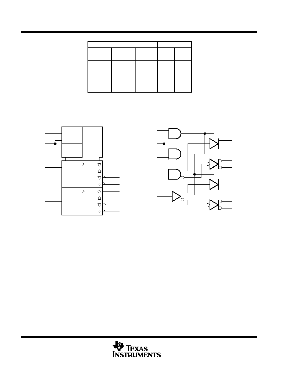
FUNCTION TABLE
INPUTS
OUTPUTS
OUTPUT
CONTROL
DATA
AND
NAND
C
CONTROL
CC
A
B
Y
Z
L
X
X
X
Z
Z
X
L
X
X
Z
Z
H
H
L
X
L
H
H
H
X
L
L
H
H
H
H
H
H
L
H = high level, L = low level, X = irrelevant,
Z = high impedance (off)
B input and 4th line of function table are applicable only to
driver number 1.
logic symbol
2
2
2
2
1
1
1
1
2ZS
2ZP
2YS
2YP
1ZS
1ZP
1YS
1YP
11
6
5
10
9
7
&
&
&
2A
1B
1A
2C
CC
1C
14
15
13
12
2
1
3
4
EN2
EN1
This symbol is in accordance with ANSI/IEEE Std 91-1984 and
IEC Publication 617-12.
Pin numbers shown are for the J, N, and W packages.
logic diagram (positive logic)
2A
1B
1A
2C
CC
1C
11
6
5
10
9
7
2ZS
2ZP
2YS
2YP
1ZS
1ZP
1YS
1YP
14
15
13
12
2
1
3
4
SN55113, SN75113
DUAL DIFFERENTIAL LINE DRIVERS
SLLS070C ≠ SEPTEMBER 1973 ≠ REVISED MARCH 1997
3
POST OFFICE BOX 655303
∑
DALLAS, TEXAS 75265
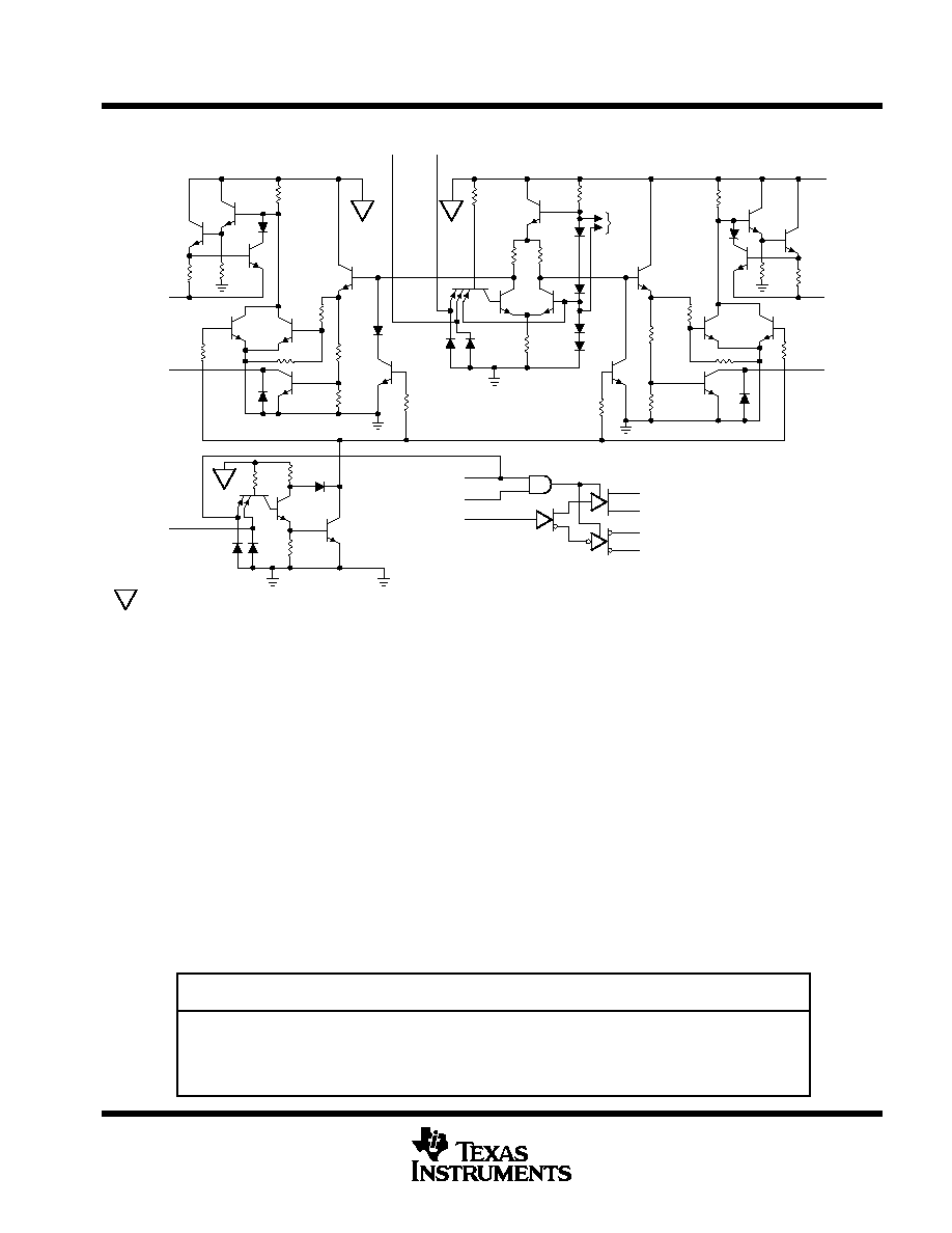
schematic
1ZP
Pullup
V
V
V
AND
Pullup
1YP
9
4 k
1 k
900
100
5 k
90
500
Input 1B
6
1YS
Output
Sink
AND
4
3
100
Output
Control
1C
4 k
1.6 k
1 k
8
GND
Common Output
Control CC
Output Control 2C
Input 2A
9
10
11
12
AND Pullup 2YP
13
AND Output 2YS
15
NAND Pullup 2ZP
14
NAND Output 2ZS
333
100
500
90
900
600
600
5 k
4 k
600
1 k
To
Other
Driver
Input 1A
5
4 k
9
100
VCC
NAND
Output
Sink
NAND
1ZS
16
2
1
V ... VCC bus
7
These components are common to both drivers. Resistor values shown are nominal and in ohms.
absolute maximum ratings over operating free-air temperature range (unless otherwise noted)
Supply voltage, V
CC
(see Note 1)
7 V
. . . . . . . . . . . . . . . . . . . . . . . . . . . . . . . . . . . . . . . . . . . . . . . . . . . . . . . . . . . . .
Input voltage, V
I
5.5 V
. . . . . . . . . . . . . . . . . . . . . . . . . . . . . . . . . . . . . . . . . . . . . . . . . . . . . . . . . . . . . . . . . . . . . . . . . .
Off-state voltage applied to open-collector outputs
12 V
. . . . . . . . . . . . . . . . . . . . . . . . . . . . . . . . . . . . . . . . . . . . .
Continuous total power dissipation (see Note 2)
See Dissipation Rating Table
. . . . . . . . . . . . . . . . . . . . . . . . . .
Operating free-air temperature range, T
A
: SN55113
≠ 55
∞
C to 125
∞
C
. . . . . . . . . . . . . . . . . . . . . . . . . . . . . . . . . .
SN75113 0
∞
C to 70
∞
C
. . . . . . . . . . . . . . . . . . . . . . . . . . . . . . . . . . . . .
Storage temperature range, T
stg
≠ 65
∞
C to 150
∞
C
. . . . . . . . . . . . . . . . . . . . . . . . . . . . . . . . . . . . . . . . . . . . . . . . . . .
Lead temperature 1,6 mm (1/16 inch) from case for 10 seconds: N package
260
∞
C
. . . . . . . . . . . . . . . . . . . . .
Case temperature for 60 seconds: FK package
260
∞
C
. . . . . . . . . . . . . . . . . . . . . . . . . . . . . . . . . . . . . . . . . . . . . .
Lead temperature 1,6 mm (1/16 inch) from case for 60 seconds: J or W package
300
∞
C
. . . . . . . . . . . . . . . .
Stresses beyond those listed under "absolute maximum ratings" may cause permanent damage to the device. These are stress ratings only, and
functional operation of the device at these or any other conditions beyond those indicated under "recommended operating conditions" is not
implied. Exposure to absolute-maximum-rated conditions for extended periods may affect device reliability.
DISSIPATION RATING TABLE
PACKAGE
TA
25
∞
C
POWER RATING
DERATING FACTOR
ABOVE TA = 25
∞
C
TA = 70
∞
C
POWER RATING
TA = 125
∞
C
POWER RATING
FK
1375 mW
11.0 mW/
∞
C
880 mW
275 mW
J
1375 mW
11.0 mW/
∞
C
880 mW
275 mW
N
1150 mW
9.2 mW/
∞
C
736 mW
N/A
W
1000 mW
8.0 mW/
∞
C
640 mW
200 mW
SN55113, SN75113
DUAL DIFFERENTIAL LINE DRIVERS
SLLS070C ≠ SEPTEMBER 1973 ≠ REVISED MARCH 1997
4
POST OFFICE BOX 655303
∑
DALLAS, TEXAS 75265
recommended operating conditions
SN55113
SN75113
UNIT
MIN
NOM
MAX
MIN
NOM
MAX
UNIT
Supply voltage, VCC
4.5
5
5.5
4.75
5
5.25
V
High-level input voltage, VIH
2
2
V
Low-level input voltage, VIL
0.8
0.8
V
High-level output current, IOH
≠ 40
≠ 40
mA
Low-level output current, IOL
40
40
mA
Operating free-air temperature, TA
≠ 55
125
0
70
∞
C
electrical characteristics over recommended operating free-air temperature range (unless
otherwise noted)
PARAMETER
TEST CONDITIONS
SN55113
SN75113
UNIT
PARAMETER
TEST CONDITIONS
MIN
TYP
MAX
MIN
TYP
MAX
UNIT
VIK
Input clamp voltage
VCC = MIN,
II = ≠ 12 mA
≠ 0.9
≠ 1.5
≠ 0.9
≠ 1.5
V
VOH
High-level output
VCC = MIN,
VIH = 2 V,
IOH = ≠10 mA
2.4
3.4
2.4
3.4
V
VOH
g
voltage
CC
,
VIL = 0.8 V
IH
,
IOH = ≠ 40 mA
2
3.0
2
3.0
V
VOL
Low-level output
VCC = MIN,
VIH = 2 V,
VIL = 0.8 V,
0 23
0 4
0 23
0 4
V
VOL
voltage
CC
,
IOL = 40 mA
IH
,
VIL 0.8 V,
0.23
0.4
0.23
0.4
V
VOK
Output clamp voltage
VCC = MAX,
IO = ≠ 40 mA
≠1.1
≠1.5
≠1.1
≠1.5
V
VOH = 12 V
TA = 25
∞
C
1
10
IO( ff)
Off-state
open collector output
VCC = MAX
VOH = 12 V
TA = 125
∞
C
200
µ
A
IO(off) open-collector output
current
VCC = MAX
VOH = 5 25 V
TA = 25
∞
C
1
10
µ
A
current
VOH = 5.25 V
TA = 70
∞
C
20
TA = 25
∞
C, VO = 0 to VCC
±
10
±
10
Off-state
VCC = MAX,
O t
t
VO = 0
≠ 150
≠ 20
IOZ
Off state
(high-impedance-state)
Output
controls at
TA = MAX
VO = 0.4 V
±
80
±
20
µ
A
output current
controls at
0.8 V
TA = MAX
VO = 2.4 V
±
80
±
20
VO = VCC
80
20
II
Input current
at maximum
A, B, C
VCC = MAX
VI = 5 5 V
1
1
mA
II
at maximum
input voltage
CC
VCC = MAX,
VI = 5.5 V
2
2
mA
IIH
High-level
A, B, C
VCC = MAX
VI = 2 4 V
40
40
µ
A
IIH
g
input current
CC
VCC = MAX,
VI = 2.4 V
80
80
µ
A
IIL
Low-level
A, B, C
VCC = MAX
VI = 0 4 V
≠ 1.6
≠ 1.6
mA
IIL
input current
CC
VCC = MAX,
VI = 0.4 V
≠ 3.2
≠ 3.2
mA
IOS
Short-circuit
VCC = MAX
VO = 0
TA = 25
∞
C
40
90
120
40
90
120
mA
IOS
output currentß
VCC = MAX,
VO = 0,
TA = 25
∞
C
≠ 40
≠ 90
≠ 120
≠ 40
≠ 90
≠ 120
mA
ICC
Supply current
All inputs at 0 V, No load,
VCC = MAX
47
65
47
65
mA
ICC
y
(both drivers)
TA = 25
∞
C
VCC = 7 V
65
85
65
85
mA
All parameters with the exception of off-state open-collector output current are measured with the active pullup connected to the sink output. For
conditions shown as MIN or MAX, use the appropriate value specified under recommended operating conditions.
All typical values are at TA = 25
∞
C and VCC = 5 V, with the exception of VCC at 7 V.
ß Only one output should be shorted at a time, and duration of the short-circuit should not exceed one second.
SN55113, SN75113
DUAL DIFFERENTIAL LINE DRIVERS
SLLS070C ≠ SEPTEMBER 1973 ≠ REVISED MARCH 1997
5
POST OFFICE BOX 655303
∑
DALLAS, TEXAS 75265
switching characteristics, V
CC
= 5 V, C
L
= 30 pF, T
A
= 25
∞
C
PARAMETER
TEST CONDITIONS
SN55113
SN75113
UNIT
PARAMETER
TEST CONDITIONS
MIN
TYP
MAX
MIN
TYP
MAX
UNIT
tPLH
Propagation delay time, low-to-high level output
See Figure 1
13
20
13
30
ns
tPHL
Propagation delay time, high-to-low-level output
See Figure 1
12
20
12
30
ns
tPZH
Output enable time to high level
RL = 180
, See Figure 2
7
15
7
20
ns
tPZL
Output enable time to low level
RL = 250
, See Figure 3
14
30
14
40
ns
tPHZ
Output disable time from high level
RL = 180
, See Figure 2
10
20
10
30
ns
tPLZ
Output disable time from low level
RL = 250
, See Figure 3
17
35
17
35
ns
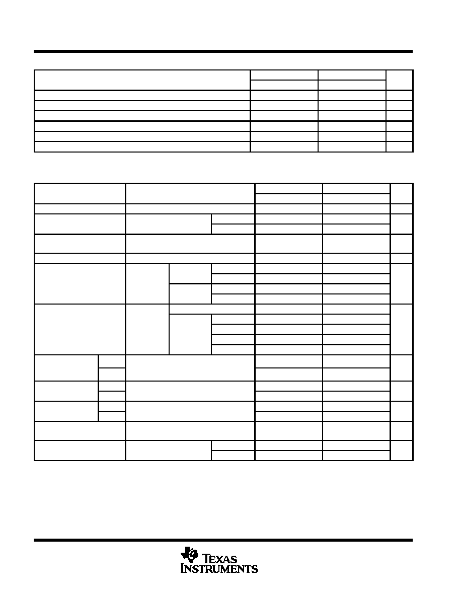
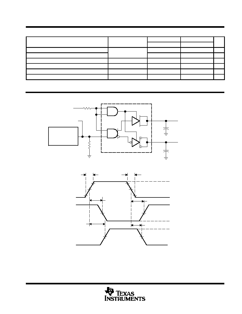
PARAMETER MEASUREMENT INFORMATION
5 ns
90%
1.5 V
10%
Input
Output
VOLTAGE WAVEFORMS
tPHL
10%
1.5 V
90%
5 ns
TEST CIRCUIT
NAND
Output
CL = 30 pF
(see Note B)
(see Note B)
CL = 30 pF
Output
AND
1 k
5 V
0 V
3 V
50
Input
(see Note A)
Generator
Pulse
VOH
1.5 V
1.5 V
tPLH
1.5 V
1.5 V
tPLH
tPHL
VOL
VOH
VOL
NAND
Output
AND
NOTES: A. The pulse generator has the following characteristics: ZO = 50
, PRR
500 kHz, tw = 100 ns.
B. CL includes probe and jig capacitance.
Figure 1. Test Circuit and Voltage Waveforms t
PLH
and t
PHL