SN55115, SN75115
DUAL DIFFERENTIAL RECEIVERS
SLLS072D ≠ SEPTEMBER 1973 ≠ REVISED MAY 1998
1
POST OFFICE BOX 655303
∑
DALLAS, TEXAS 75265
D
Choice of Open-Collector or Active Pullup
(Totem-Pole) Outputs
D
Single 5-V Supply
D
Differential Line Operation
D
Dual-Channel Operation
D
TTL Compatible
D
±
15-V Common-Mode Input Voltage Range
D
Optional-Use Built-In 130-
Line-
Terminating Resistor
D
Individual Frequency-Response Controls
D
Individual Channel Strobes
D
Designed for Use With SN55113, SN75113,
SN55114, and SN75114 Drivers
D
Designed to Be Interchangeable With
National DS9615 Line Receivers
description
The SN55115 and SN75115 dual differential line
receivers are designed to sense small differential
signals in the presence of large common-mode
noise. These devices give TTL-compatible output
signals as a function of the differential input
voltage. The open-collector output configuration
permits the wire-ANDing of similar TTL outputs
(such as SN5401/SN7401) or other
SN55115/SN75115 line receivers. This permits a
level of logic to be implemented without extra
delay.
The output stages are similar to TTL totem-pole outputs, but with sink outputs, 1YS and 2YS, and the
corresponding active pullup terminals, 1YP and 2YP, available on adjacent package pins. The frequency
response and noise immunity may be provided by a single external capacitor. A strobe input is provided for each
channel. With the strobe in the low level, the receiver is disabled and the outputs are forced to a high level.
The SN55115 is characterized for operation over the full military temperature range of ≠ 55
∞
C to 125
∞
C. The
SN75115 is characterized for operation from 0
∞
C to 70
∞
C.
FUNCTION TABLE
STRB
DIFF INPUT
(A AND B)
OUTPUT
(YP AND YS
TIED
TOGETHER)
L
X
H
H
L
H
H
H
L
H = VI
VIH min or VID more positive than VT + max
L = VI
VIL max or VID more negative thanVT ≠ max
X = irrelevant
Copyright
©
1998, Texas Instruments Incorporated
PRODUCTION DATA information is current as of publication date.
Products conform to specifications per the terms of Texas Instruments
standard warranty. Production processing does not necessarily include
testing of all parameters.
Please be aware that an important notice concerning availability, standard warranty, and use in critical applications of
Texas Instruments semiconductor products and disclaimers thereto appears at the end of this data sheet.
1
2
3
4
5
6
7
8
16
15
14
13
12
11
10
9
1YS
1YP
1STRB
1RTC
1B
1R
T
1A
GND
V
CC
2YS
2YP
2STRB
2RTC
2B
2R
T
2A
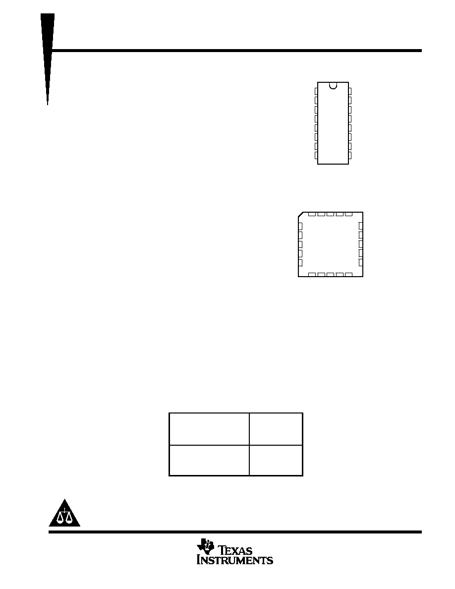
SN55115 . . . J OR W PACKAGE
SN75115 . . . N PACKAGE
(TOP VIEW)
3
2
1 20 19
9 10 11 12 13
4
5
6
7
8
18
17
16
15
14
2YP
2STRB
NC
2RTC
2B
1STRB
1RTC
NC
1B
1R
T
SN55114 . . . FK PACKAGE
(TOP VIEW)
1YP
1YS
NC
2YS
1A
GND
NC
NC ≠ No internal connection
CC
V
2A
2R
T
SN55115, SN75115
DUAL DIFFERENTIAL RECEIVERS
SLLS072D ≠ SEPTEMBER 1973 ≠ REVISED MAY 1998
2
POST OFFICE BOX 655303
∑
DALLAS, TEXAS 75265
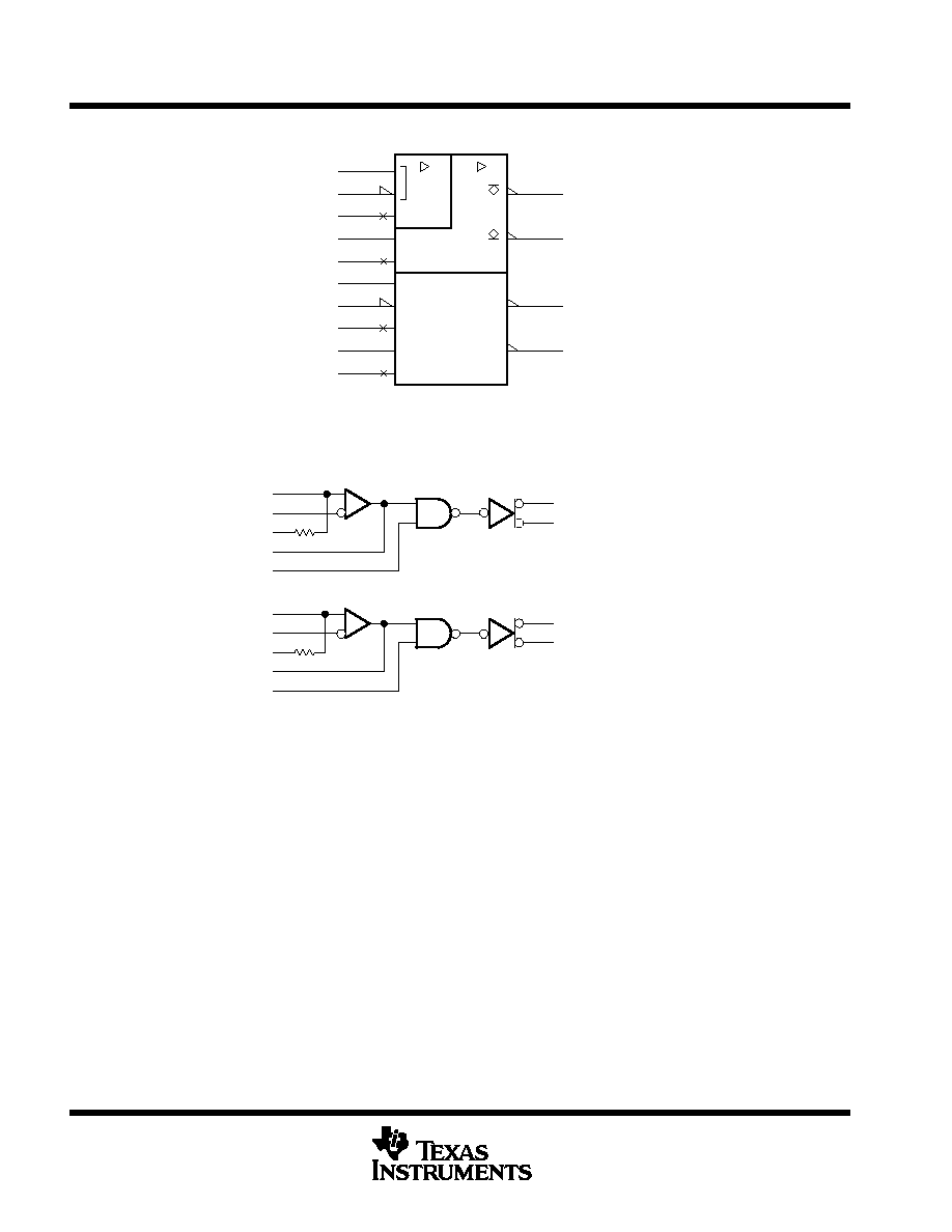
logic symbol
&
2YS
2YP
1YS
1YP
RT
RSP
12
13
10
9
11
4
3
6
7
5
2RTC
2STRB
2RT
2A
2B
1RTC
1STRB
1RT
1A
1B
15
14
1
2
This symbol is in accordance with ANSI/IEEE Std 91-1984 and IEC Publication 617-12.
logic diagram (positive logic)
11
9
10
12
13
2YP (Pullup)
2YS (Sink)
14
15
2B
2A
2RT
2RTC
2STRB
1STRB
1RTC
1RT
1A
1B
1
2 1YP (Pullup)
3
4
6
7
5
1YS (Sink)

SN55115, SN75115
DUAL DIFFERENTIAL RECEIVERS
SLLS072D ≠ SEPTEMBER 1973 ≠ REVISED MAY 1998
3
POST OFFICE BOX 655303
∑
DALLAS, TEXAS 75265
schematic (each receiver)
YS
Sink
1.64 k
130
Input 7.9
V
V
V
V
150
2.5 k
Common to
Both Receivers
A
8 k
7 k
1 pF
1.5 k
1.64 k
B
Input 5.11
130
150
150
8 k
7 k
1 pF
1 k
1 k
2.6 k
500
2.6 k
500
150
1.5 k
3 k
5 k
20
2 k
RT
6,10
Strobe
3,13
Response
Time
Control
4,12
2.7 k
16
VCC
2,14 Pullup
YP
1,15
Output
8
GND
Resistor values are nominal and in ohms.
Pin numbers shown are for the J, N, and W packages.
absolute maximum ratings over operating free-air temperature range (unless otherwise noted)
Supply voltage, V
CC
(see Note 1)
7 V
. . . . . . . . . . . . . . . . . . . . . . . . . . . . . . . . . . . . . . . . . . . . . . . . . . . . . . . . . . . . .
Input voltage V
I
(A, B, and R
T
)
±
25 V
. . . . . . . . . . . . . . . . . . . . . . . . . . . . . . . . . . . . . . . . . . . . . . . . . . . . . . . . . . . . . .
Input voltage V
I
(STRB)
5.5 V
. . . . . . . . . . . . . . . . . . . . . . . . . . . . . . . . . . . . . . . . . . . . . . . . . . . . . . . . . . . . . . . . . . . .
Off-state voltage applied to open-collector outputs
14 V
. . . . . . . . . . . . . . . . . . . . . . . . . . . . . . . . . . . . . . . . . . . . .
Continuous total power dissipation
See Dissipation Rating Table
. . . . . . . . . . . . . . . . . . . . . . . . . . . . . . . . . . . . .
Storage temperature range, T
stg
≠65
∞
C to 150
∞
C
. . . . . . . . . . . . . . . . . . . . . . . . . . . . . . . . . . . . . . . . . . . . . . . . . . .
Case temperature for 60 seconds: FK package
260
∞
C
. . . . . . . . . . . . . . . . . . . . . . . . . . . . . . . . . . . . . . . . . . . . . .
Lead temperature 1,6 mm (1/16 inch) from case for 60 seconds: J or W package
300
∞
C
. . . . . . . . . . . . . . . .
Lead temperature 1,6 mm (1/16 inch) from case for 10 seconds: N package
260
∞
C
. . . . . . . . . . . . . . . . . . . . .
Stresses beyond those listed under "absolute maximum ratings" may cause permanent damage to the device. These are stress ratings only, and
functional operation of the device at these or any other conditions beyond those indicated under "recommended operating conditions" is not
implied. Exposure to absolute-maximum-rated conditions for extended periods may affect device reliability.
NOTE 1: All voltage values, except differential input voltage, are with respect to network ground terminal.

SN55115, SN75115
DUAL DIFFERENTIAL RECEIVERS
SLLS072D ≠ SEPTEMBER 1973 ≠ REVISED MAY 1998
4
POST OFFICE BOX 655303
∑
DALLAS, TEXAS 75265
DISSIPATION RATING TABLE
PACKAGE
TA
25
∞
C
POWER RATING
DERATING FACTOR
ABOVE TA = 25
∞
C
TA = 70
∞
C
POWER RATING
TA = 125
∞
C
POWER RATING
FK
1375 mW
11.0 mW/
∞
C
880 mW
275 mW
J
1375 mW
11.0 mW/
∞
C
880 mW
275 mW
N
1150 mW
9.2 mW/
∞
C
736 mW
--
W
1000 mW
8.0 mW/
∞
C
640 mW
200 mW
In the FK, J, and W packages, SN55115 chips are either silver glass or alloy mounted. SN75115 chips are
glass mounted.
recommended operating conditions
SN55115
SN75115
UNIT
MIN
NOM
MAX
MIN
NOM
MAX
UNIT
Supply voltage, VCC
4.5
5
5.5
4.75
5
5.25
V
High-level input voltage at STRB, VIH
2.4
2.4
V
Low-level input voltage at STRB, VIL
0.4
0.4
V
High-level output current, IOH
≠ 5
≠ 5
mA
Low-level output current, IOL
15
15
mA
Operating free-air temperature, TA
≠ 55
125
0
70
∞
C

SN55115, SN75115
DUAL DIFFERENTIAL RECEIVERS
SLLS072D ≠ SEPTEMBER 1973 ≠ REVISED MAY 1998
5
POST OFFICE BOX 655303
∑
DALLAS, TEXAS 75265
electrical characteristics over recommended operating free-air temperature range (unless
otherwise noted)
PARAMETER
TEST CONDITIONS
SN55115
SN75115
UNIT
PARAMETER
TEST CONDITIONS
MIN
TYP
MAX
MIN
TYP
MAX
UNIT
VIT + ß
Positive-going
threshold voltage
VO = 0 .4 V,
IOL = 15 mA,
VIC = 0
500
500
mV
VIT ≠ ß
Negative-going
threshold voltage
VO = 2 .4 V,
IOH = ≠ 5 mA,
VIC = 0
≠ 500∂
≠ 500∂
mV
VICR
Common-mode
input voltage range
VID =
±
1 V
+ 15
to
≠ 15
+ 24
to
≠ 19
+ 15
to
≠ 15
+ 24
to
≠ 19
V
Hi h l
l
t
V
MIN
V
0 5 V
TA = MIN
2.2
2.4
VOH
High-level ouput
voltage
VCC = MIN,
IOH = ≠ 5 mA
VID = ≠ 0.5 V,
TA = 25
∞
C
2.4
3.4
2.4
3.4
V
voltage
IOH = ≠ 5 mA
TA = MAX
2.4
2.4
VOL
Low-level output
voltage
VCC = MIN,
IOL = 15 mA
VID = ≠ 0.5 V,
0.22
0.4
0.22
0.45
V
L
l
l i
t
V
MAX
V
0 4 V
TA = MIN
≠ 0.9
≠ 0.9
IIL
Low-level input
current
VCC = MAX,
VI = 0.4 V,
Other input at 5 5 V
TA = 25
∞
C
≠ 0.5
≠ 0.7
≠ 0.5
≠ 0.7
mA
current
Other in ut at 5.5 V
TA = MAX
≠ 0.7
≠ 0.7
ISH
High-level strobe
VCC = MIN,
VID = ≠ 0.5 V,
TA = 25
∞
C
2
5
µ
A
ISH
g
current
CC
,
Vstrobe = 4.5 V
ID
,
TA = MAX
5
10
µ
A
ISL
Low-level strobe
current
VCC = MAX,
Vstrobe = 0.4 V
VID = 0.5 V,
TA = 25
∞
C
≠ 1.15
≠ 2.4
≠ 1.15
≠ 2.4
mA
I(RTC)
Response-time-
control current
VCC = MAX,
VRC = 0
VID = 0.5 V,
TA = 25
∞
C
≠ 1.2
≠ 3.4
≠ 1.2
≠ 3.4
mA
VCC = MIN,
VOH = 12 V,
TA = 25
∞
C
100
IO(off)
Off-state
open collector
CC
,
VID = ≠ 4.5 V
OH
,
TA = MAX
200
µ
A
IO(off)
open-collector
output current
VCC = MIN,
VOH = 5.25 V, TA = 25
∞
C
100
µ
A
out ut current
CC
,
VID = ≠ 4.75 V
OH
,
TA = MAX
200
RT
Line-terminating
resistance
VCC = 5 V
TA = 25
∞
C
77
130
167
74
130
179
IOS
Supply-circuit output
current #
VCC = MAX,
VO = 0
VID = ≠ 0.5 V,
TA = 25
∞
C
≠ 15
≠ 40
≠ 80
≠ 14
≠ 40
≠ 100
mA
ICC
Supply current
(both receivers)
VCC = MAX,
VIC = 0
VID = 0.5 V,
TA = 25
∞
C
32
50
32
50
mA
Unless otherwise noted, Vstrobe = 2.4 V. All parameters with the exception of off-state open-collector output current are measured with the active
pullup connected to the sink output.
All typical values are at VCC = 5 V, TA = 25
∞
C, and VIC = 0.
ß Differential voltages are at the B input terminal with respect to the A input terminal.
∂ The algebraic convention, in which the less positive (more negative) limit is designated as minimum, is used in this data sheet for threshold
voltages only.
# Only one output should be shorted to ground at a time, and duration of the short circuit should not exceed one second.