
LT1013, LT1013A, LT1013D
DUAL PRECISION OPERATIONAL AMPLIFIERS
SLOS018H - MAY 1988 - REVISED NOVEMBER 2004
1
POST OFFICE BOX 655303
∑
DALLAS, TEXAS 75265
D
Single-Supply Operation
- Input Voltage Range Extends to Ground
- Output Swings to Ground While Sinking
Current
D
Input Offset Voltage
- 150
µ
V Max at 25
∞
C for LT1013A
D
Offset-Voltage Temperature Coefficient
- 2.5
µ
V/
∞
C Max for LT1013A
D
Input Offset Current
- 0.8 nA Max at 25
∞
C for LT1013A
D
High Gain . . . 1.5 V/
µ
V Min (R
L
= 2 k
),
0.8 V/
µ
V Min (R
L
= 600 k
) for LT1013A
D
Low Supply Current . . . 0.5 mA Max at
T
A
= 25
∞
C for LT1013A
D
Low Peak-to-Peak Noise Voltage . . . 0.55
µ
V
Typ
D
Low Current Noise . . . 0.07 pA/
Hz Typ
description/ordering information
The LT1013 devices are dual precision
operational amplifiers, featuring high gain, low
supply current, low noise, and low-offset-voltage
temperature coefficient.
The LT1013 devices can be operated from a
single 5-V power supply; the common-mode input
voltage range includes ground, and the output can
also swing to within a few millivolts of ground.
Crossover distortion is eliminated. The LT1013
can be operated with both dual
±
15-V and single
5-V supplies.
The LT1013C, LT1013AC, and LT1013D are characterized for operation from 0
∞
C to 70
∞
C. The LT1013I,
LT1013AI, and LT1013DI are characterized for operation from -40
∞
C to 105
∞
C. The LT1013M, LT1013AM, and
LT1013DM are characterized for operation over the full military temperature range of -55
∞
C to 125
∞
C.
Copyright
2004, Texas Instruments Incorporated
PRODUCTION DATA information is current as of publication date.
Products conform to specifications per the terms of Texas Instruments
standard warranty. Production processing does not necessarily include
testing of all parameters.
Please be aware that an important notice concerning availability, standard warranty, and use in critical applications of
Texas Instruments semiconductor products and disclaimers thereto appears at the end of this data sheet.
1
2
3
4
8
7
6
5
1IN+
V
CC-
2IN+
2IN-
1IN-
1OUT
V
CC+
2OUT
LT1013, LT1013D . . . D PACKAGE
(TOP VIEW)
3
2
1 20 19
9 10 11 12 13
4
5
6
7
8
18
17
16
15
14
NC
2OUT
NC
2IN-
NC
NC
1IN-
NC
1IN+
NC
LT1013, LT1013A . . . FK PACKAGE
(TOP VIEW)
NC
1OUT
NC
NC
NC
NC
NC
2IN+
CC+
V
CC-
V
1
2
3
4
8
7
6
5
1OUT
1IN-
1IN+
V
CC-
V
CC+
2OUT
2IN-
2IN+
LT1013, LT1013D . . . JG OR P PACKAGE
(TOP VIEW)
NC - No internal connection
On products compliant to MIL PRF 38535, all parameters are tested
unless otherwise noted. On all other products, production
processing does not necessarily include testing of all parameters.
LT1013, LT1013A, LT1013D
DUAL PRECISION OPERATIONAL AMPLIFIERS
SLOS018H - MAY 1988 - REVISED NOVEMBER 2004
2
POST OFFICE BOX 655303
∑
DALLAS, TEXAS 75265
ORDERING INFORMATION
TA
VIOmax
AT 25
∞
C
(
µ
V)
PACKAGE
ORDERABLE
PART NUMBER
TOP-SIDE
MARKING
P-DIP (P)
Tube of 50
LT1013CP
LT1013P
300
SOIC (D)
Tube of 75
LT1013CD
1013C
0
∞
C to 70
∞
C
300
SOIC (D)
Reel of 2500
LT1013CDR
1013C
0
∞
C to 70
∞
C
P-DIP (P)
Tube of 50
LT1013DP
LT1013DP
800
SOIC (D)
Tube of 75
LT1013DD
1013D
800
SOIC (D)
Reel of 2500
LT1013DDR
1013D
P-DIP (P)
Tube of 50
LT1013DIP
LT1013DIP
-40
∞
C to 105
∞
C
800
SOIC (D)
Tube of 75
LT1013DID
1013DI
-40 C to 105 C
800
SOIC (D)
Reel of 2500
LT1013DIDR
1013DI
C-DIP (JG)
Tube of 50
LT1013AMJG
LT1013AMJG
150
C-DIP (JGB)
Tube of 50
LT1013AMJGB
LT1013AMJGB
150
LCCC (FK)
Tube of 55
LT1013AMFK
LT1013AMFK
-55
∞
C to 125
∞
C
LCCC (FKB)
Tube of 55
LT1013AMFKB
LT1013AMFKB
-55
∞
C to 125
∞
C
C-DIP (JG)
Tube of 50
LT1013MJG
LT1013MJG
300
C-DIP (JGB)
Tube of 50
LT1013MJGB
LT1013MJGB
300
LCCC (FKB)
Tube of 55
LT1013MFKB
LT1013MFKB
800
SOIC (D)
Tube of 75
LT1013DMD
1013DM
Package drawings, standard packing quantities, thermal data, symbolization, and PCB design guidelines are
available at www.ti.com/sc/package.
LT1013, LT1013A, LT1013D
DUAL PRECISION OPERATIONAL AMPLIFIERS
SLOS018H - MAY 1988 - REVISED NOVEMBER 2004
POST OFFICE BOX 655303 DALLAS, TEXAS 75265
∑
3
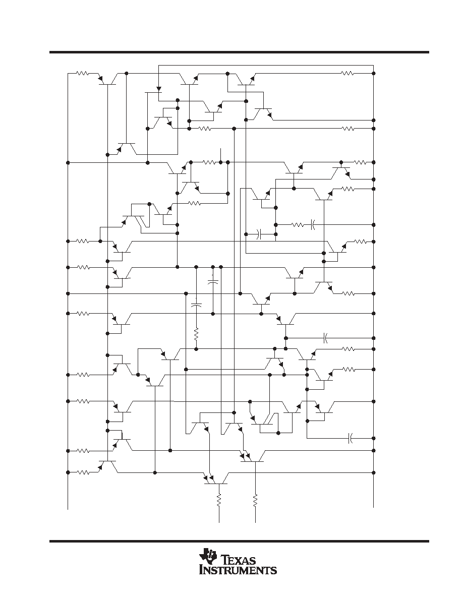
schematic
(each amplifier)
OUT
600
J1
800
V
CC-
VCC+
IN-
IN+
30
42 k
Q40
Q39
Q41
Q38
14 k
Q37
Q35
3.9 k
75 pF
5 k
5 k
2 k
1.3 k
2 k
Q24
Q23
Q34
21 pF
2.5 pF
2.4 k
18
Q26
Q33
Q25
Q30
Q32
Q15
Q14
Q16
Q13
Q6
Q5
9 k
9 k
1.6 k
1.6 k
1.6 k
100
1 k
Q3
Q4
400
400
Q1
Q21
Q22
Q2
Q12
Q29
Q1
1
Q9
Q7
Q8
10 pF
Q10
Q18
Q19
2 k
10 pF
Q27
Q28
4 pF
Q31
Q17
Q36
Q20
Component values are nominal.

LT1013, LT1013A, LT1013D
DUAL PRECISION OPERATIONAL AMPLIFIERS
SLOS018H - MAY 1988 - REVISED NOVEMBER 2004
4
POST OFFICE BOX 655303
∑
DALLAS, TEXAS 75265
absolute maximum ratings over operating free-air temperature range (unless otherwise noted)
Supply voltage (see Note 1): V
CC+
22
V
. . . . . . . . . . . . . . . . . . . . . . . . . . . . . . . . . . . . . . . . . . . . . . . . . . . . . . . . . .
V
CC-
-22
V
. . . . . . . . . . . . . . . . . . . . . . . . . . . . . . . . . . . . . . . . . . . . . . . . . . . . . . . . .
Input voltage range, V
I
(any input, see Note 1)
V
CC-
- 5 V to V
CC+
. . . . . . . . . . . . . . . . . . . . . . . . . . . . . . . . . . .
Differential input voltage (see Note 2)
±
30 V
. . . . . . . . . . . . . . . . . . . . . . . . . . . . . . . . . . . . . . . . . . . . . . . . . . . . . . . .
Duration of short-circuit current at (or below) 25
∞
C (see Note 3)
Unlimited
. . . . . . . . . . . . . . . . . . . . . . . . . . . . . .
Package thermal impedance,
JA
(see Notes 4 and 5): D package
97
∞
C/W
. . . . . . . . . . . . . . . . . . . . . . . . . . . .
P package
85
∞
C/W
. . . . . . . . . . . . . . . . . . . . . . . . . . . .
Operating virtual junction temperature, T
J
150
∞
C
. . . . . . . . . . . . . . . . . . . . . . . . . . . . . . . . . . . . . . . . . . . . . . . . . . .
Case temperature for 60 seconds: FK package
260
∞
C
. . . . . . . . . . . . . . . . . . . . . . . . . . . . . . . . . . . . . . . . . . . . . .
Lead temperature 1,6 mm (1/16 inch) from case for 10 seconds: JG package
300
∞
C
. . . . . . . . . . . . . . . . . . . .
Storage temperature range, T
stg
-65
∞
C to 150
∞
C
. . . . . . . . . . . . . . . . . . . . . . . . . . . . . . . . . . . . . . . . . . . . . . . . . . .
Stresses beyond those listed under "absolute maximum ratings" may cause permanent damage to the device. These are stress ratings only, and
functional operation of the device at these or any other conditions beyond those indicated under "recommended operating conditions" is not
implied. Exposure to absolute-maximum-rated conditions for extended periods may affect device reliability.
NOTES:
1. All voltage values, except differential voltages, are with respect to the midpoint between VCC+ and VCC-.
2. Differential voltages are at IN+ with respect to IN-.
3. The output may be shorted to either supply.
4. Maximum power dissipation is a function of TJ(max),
JA, and TA. The maximum allowable power dissipation at any allowable
ambient temperature is PD = (TJ(max) - TA)/
JA. Operating at the absolute maximum TJ of 150
∞
C can affect reliability. Due to
variation in individual device electrical characteristics and thermal resistance, the built-in thermal overload protection may be
activated at power levels slightly above or below the rated dissipation.
5. The package thermal impedance is calculated in accordance with JESD 51-7.
LT1013, LT1013A, LT1013D
DUAL PRECISION OPERATIONAL AMPLIFIERS
SLOS018H - MAY 1988 - REVISED NOVEMBER 2004
POST OFFICE BOX 655303 DALLAS, TEXAS 75265
∑
5
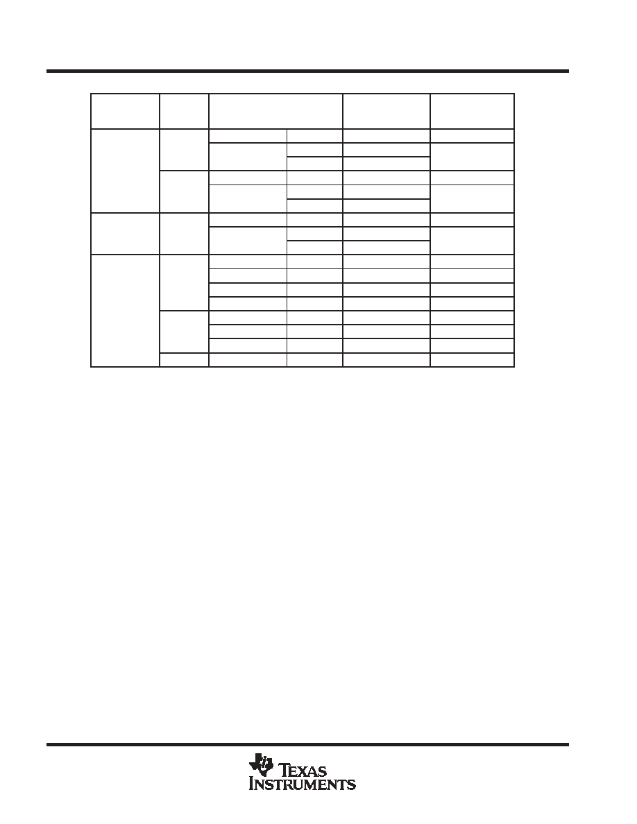
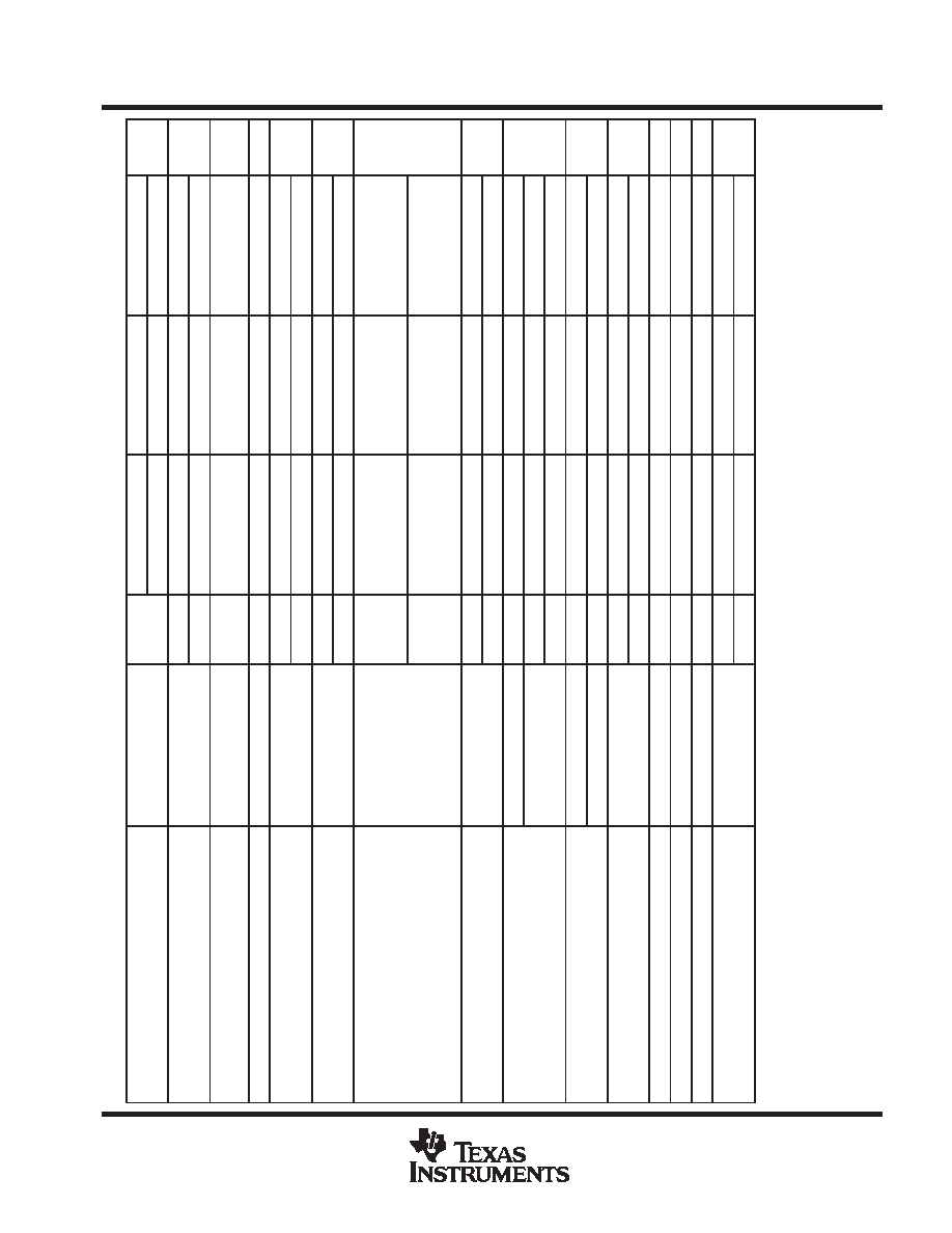
electrical characteristics at specified free-air temperature, V
CC
±
=
±
15 V
,
V
IC
= 0 (unless otherwise noted)
P
ARAMETER
TEST CONDITIONS
T
A
L
T1013C
L
T1013AC
L
T1013DC
UNIT
P
ARAMETER
TEST CONDITIONS
T
A
MIN
TYP
MAX
MIN
TYP
MAX
MIN
TYP
MAX
UNIT
V
IO
Input of
fset voltage
R
S
= 50
25
∞
C
60
300
40
150
200
800
V
V
IO
Input of
fset voltage
R
S
= 50
Full range
400
240
1000
µ
V
a
V
T
emperature coef
ficient of input
Full range
0.4
2.5
0.3
2
0.7
5
V/
∞
C
a
V
IO
T
emperature coef
ficient of input
of
fset voltage
Full range
0.4
2.5
0.3
2
0.7
5
µ
V/
∞
C
Long-term drift of input of
fset voltage
25
∞
C
0.5
0.4
0.5
µ
V/mo
I IO
Input of
fset current
25
∞
C
0.2
1.5
0.15
0.8
0.2
1.5
nA
I IO
Input of
fset current
Full range
2.8
1.5
2.8
nA
I IB
Input bias current
25
∞
C
-15
-30
-12
-20
-15
-30
nA
I IB
Input bias current
Full range
-38
-25
-38
nA
-15
-15.3
-15
-15.3
-15
-15.3
25
∞
C
-15
to
13.5
-15.3
to
13.8
-15
to
13.5
-15.3
to
13.8
-15
to
13.5
-15.3
to
13.8
V
ICR
Common-mode input voltage range
25
C
to
13.5
to
13.8
to
13.5
to
13.8
to
13.5
to
13.8
V
V
ICR
Common-mode input voltage range
-15
-15
-15
V
Full range
-15
to
13
-15
to
13
-15
to
13
Full range
to
13
to
13
to
13
V
OM
Maximum peak output voltage swing
R
L
= 2 k
25
∞
C
±
12.5
±
14
±
13
±
14
±
12.5
±
14
V
V
OM
Maximum peak output voltage swing
R
L
= 2 k
Full range
±
12
±
12.5
±
12
V
Large-signal dif
ferential voltage
V
O
=
±
10 V
,
R
L
= 600
25
∞
C
0.5
0.2
0.8
2.5
0.5
2
A
VD
Large-signal dif
ferential voltage
amplification
V
O
=
±
10 V
,
R
L
= 2 k
25
∞
C
1.2
7
1.5
8
1.2
7
V/
µ
V
A
VD
amplification
V
O
=
±
10 V
,
R
L
= 2 k
Full range
0.7
1
0.7
V/
µ
V
CMRR
Common-mode rejection ratio
V
IC
= -15 V to 13.5 V
25
∞
C
97
11
4
100
11
7
97
11
4
dB
CMRR
Common-mode rejection ratio
V
IC
= -14.9 V to 13 V
Full range
94
98
94
dB
k
SVR
Supply-voltage rejection ratio
V
CC+
=
±
2 V to
±
18 V
25
∞
C
100
11
7
103
120
100
11
7
dB
k
SVR
Supply-voltage rejection ratio
(
V
CC
/
V
IO
)
V
CC+
=
±
2 V to
±
18 V
Full range
97
101
97
dB
Channel separation
V
O
=
±
10 V
,
R
L
= 2 k
25
∞
C
120
137
123
140
120
137
dB
r id
Dif
ferential input resistance
25
∞
C
70
300
100
400
70
300
M
r ic
Common-mode input resistance
25
∞
C
4
5
4
G
I CC
Supply current per amplifier
25
∞
C
0.35
0.55
0.35
0.5
0.35
0.55
mA
I CC
Supply current per amplifier
Full range
0.7
0.55
0.6
mA
Full range is 0
∞
C to 70
∞
C.
All typical values are at T
A
= 25
∞
C.