1
Data sheet acquired from Harris Semiconductor
SCHS206B
Features
∑ Synchronous Programmable
˜
N Counter N = 3 to 9999
or 15999
∑ Presettable Down-Counter
∑ Fully Static Operation
∑ Mode-Select Control of Initial Decade Counting
Function (
˜
10, 8, 5, 4, 2)
∑ Master Preset Initialization
∑ Latchable
˜
N Output
∑ Fanout (Over Temperature Range)
- Standard Outputs . . . . . . . . . . . . . . . 10 LSTTL Loads
- Bus Driver Outputs . . . . . . . . . . . . . 15 LSTTL Loads
∑ Wide Operating Temperature Range . . . -55
o
C to 125
o
C
∑ Balanced Propagation Delay and Transition Times
∑ Significant Power Reduction Compared to LSTTL
Logic ICs
∑ HC Types
- 2V to 6V Operation
- High Noise Immunity: N
IL
= 30%, N
IH
= 30% of V
CC
at V
CC
= 5V
Applications
∑ Communications Digital Frequency Synthesizers;
VHF, UHF, FM, AM, etc.
∑ Fixed or Programmable Frequency Division
∑ "Time Out" Timer for Consumer-Application Industrial
Controls
Description
The 'HC4059 are high-speed silicon-gate devices that are
pin-compatible with the CD4059A devices of the CD4000B
series. These devices are divide-by-N down-counters that
can be programmed to divide an input frequency by any
number "N" from 3 to 15,999. The output signal is a pulse
one clock cycle wide occurring at a rate equal to the input
frequency divide by N. The down-counter is preset by means
of 16 jam inputs.
The three Mode-Select Inputs K
a
, K
b
and K
c
determine the
modulus ("divide-by" number) of the first and last counting
sections in accordance with the truth table. Every time the first
(fastest) counting section goes through one cycle, it reduces by
1 the number that has been preset (jammed) into the three
decades of the intermediate counting section an the last
counting section, which consists of flip-flops that are not
needed for opening the first counting section. For example, in
the
˜
2 mode, only one flip-flop is needed in the first counting
section. Therefore the last counting section has three flip-flops
that can be preset to a maximum count of seven with a place
value of thousands. If
˜
10 is desired for the first section, K
a
is
set "high", K
b
"high" and K
c
"low". Jam inputs J1, J2, J3, and J4
are used to preset the first counting section and there is no last
counting section. The intermediate counting section consists of
three cascaded BCD decade (
˜
10) counters presettable by
means of Jam Inputs J5 through J16.
The
Mode-Select
Inputs
permit
frequency-synthesizer
channel separations of 10, 12.5, 20, 25 or 50 parts. These
inputs set the maximum value of N at 9999 (when the first
counting section divides by 5 or 10) or 15,999 (when the first
counting section divides by 8, 4, or 2).
The three decades of the intermediate counter can be preset
to a binary 15 instead of a binary 9, while their place values
are still 1, 10, and 100, multiplied by the number of the
˜
N
mode. For example, in the
˜
8 mode, the number from which
counting down begins can be preset to:
3rd Decade
1500
2nd Decade
150
1st Decade
15
Last Counting Section
1000
The total of these numbers (2665) times 8 equals 12,320.
The first counting section can be preset to 7. Therefore,
21,327 is the maximum possible count in the
˜
8 mode.
The highest count of the various modes is shown in the
Extended Counter Range column. Control inputs K
b
and K
c
can be used to initiate and lock the counter in the "master
preset" state. In this condition the flip-flops in the counter are
preset in accordance with the jam inputs and the counter
remains in that state as long as K
b
and K
c
both remain low. The
counter begins to count down from the preset state when a
counting mode other than the master preset mode is selected.
Ordering Information
PART NUMBER
TEMP. RANGE
(
o
C)
PACKAGE
CD54HC4059F3A
-55 to 125
24 Ld CERDIP
CD74HC4059E
-55 to 125
24 Ld PDIP
CD74HC4059M96
-55 to 125
24 Ld SOIC
NOTE: When ordering, use the entire part number. The suffix 96
denotes tape and reel.
February 1998 - Revised May 2003
CAUTION: These devices are sensitive to electrostatic discharge. Users should follow proper IC Handling Procedures.
Copyright
©
2003, Texas Instruments Incorporated
CD54HC4059, CD74HC4059
High-Speed CMOS Logic
CMOS Programmable Divide-by-N Counter
[ /Title
(CD74
HC4059
)
/Sub-
ject
(High-
Speed
CMOS
Logic
CMOS
Pro-

2
The counter should always be put in the master preset mode
before the
˜
5 mode is selected. Whenever the master preset
mode is used, control signals K
b
= "low" and K
c
= "low" must
be applied for at least 3 full clock pulses.
After Preset Mode inputs have been changed to one of the
˜
modes, the next positive-going clock transition changes an
internal flip-flop so that the countdown can begin at the
second positive-going clock transition. Thus, after an MP
(Master Preset) mode, there is always one extra count
before the output goes high. Figure 1 illustrates a total count
of 3 (
˜
8 mode). If the Master Preset mode is started two
clock cycles or less before an output pulse, the output pulse
will appear at the time due. If the Master Preset Mode is not
used, the counter jumps back to the "Jam" count when the
output pulse appears.
A "high" on the Latch Enable input will cause the counter
output to remain high once an output pulse occurs, and to
remain in the high state until the latch input returns to "low".
If the Latch Enable is "low", the output pulse will remain high
for only one cycle of the clock-input signal.
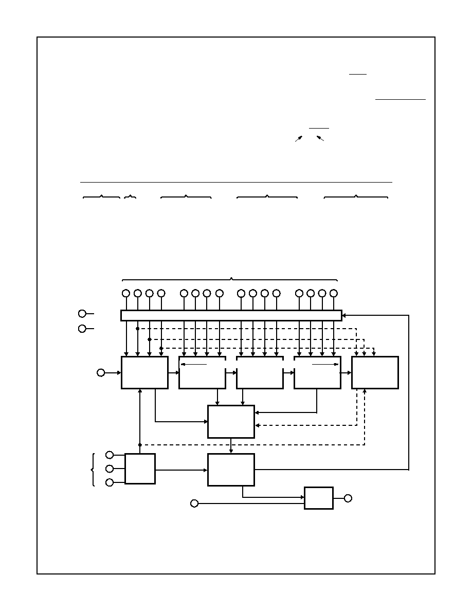
Pinout
CD54HC4059
(CERDIP)
CD74HC4059
(PDIP, SOIC)
TOP VIEW
Functional Diagram
1
2
3
4
5
6
7
8
9
10
11
12
CP
LE
J1
J2
J3
J4
J16
J15
J14
J13
K
c
GND
16
17
18
19
20
21
22
23
24
15
14
13
V
CC
J5
J6
J7
J8
J10
J12
K
a
K
b
Q
J9
J11
Q =
K
c
LE
K
b
K
a
CP
J1 - J16
f
IN
N
-------
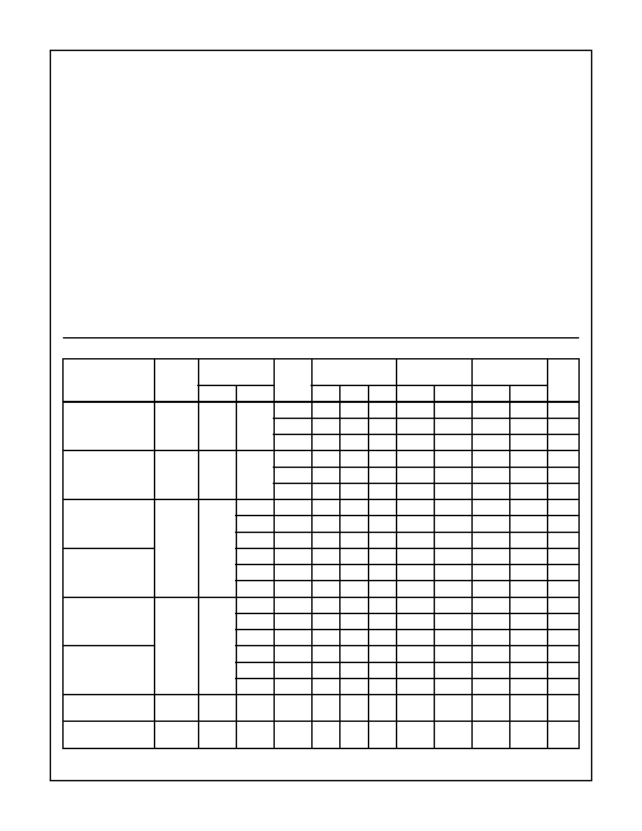
TRUTH TABLE
MODE SELECT INPUT
FIRST COUNTING SECTION
LAST COUNTING SECTION
COUNTER RANGE
DESIGN
EXTENDED
K
a
K
b
K
c
MODE
DIVIDES-BY
CAN BE
PRESET
TO A MAX
OF:
(NOTE 1)
JAM
INPUTS
USED:
MODE
DIVIDES-BY
CAN BE
PRESET
TO A MAX
OF:
(NOTE 1)
JAM
INPUTS
USED:
MAX
MAX
H
H
H
2
1
J1
8
7
J2, J3, J4
15,999
17,331
L
H
H
4
3
J1, J2
4
3
J3, J4
15,999
18,663
H
L
H
5
(Note 2)
4
J1, J2, J3
2
1
J4
9,999
13,329
L
L
H
8
7
J1, J2, J3
2
1
J4
15,999
21,327
H
H
L
10
9
J1, J2, J3, J4
1
0
-
9,999
16,659
X
L
L
Master Preset
Master Preset
-
-
X = Don't care
NOTES:
1. J1 = Least Significant Bit. J4 = Most Significant Bit.
2. Operation in the 5mode (1st counting section) requires going through the Master Preset mode prior to going into the 5mode. At power
turn-on, Kc must be "low" for a period of 3 input clock pulses after VCC reaches a minimum of 3V.
CD54HC4059, CD74HC4059
CD54HC4059, CD74HC4059
3
How to Preset the HC/HCT4059 to Desired
˜
N
The value N is determined as follows:
To calculate preset values for any N count, divide the N
count by the Mode. The resultant is the corresponding
preset values of the 5th through 2nd decade with the
remainder being equal to the 1st decade value.
NOTE: To verify the results, use Equation 1:
N = 5 (1000 x 1 + 100 x 6 + 10 x 9 + 1 x 5) + 4
N = 8479
N = (MODE
) (1000 x Decade 5 Preset + 100 x Decade 4
Preset + 10 x Decade 3 Preset + 1 x Decade 2 Preset) +
Decade 1 Preset
MODE = First counting section divider (10, 8, 5, 4 or 2)
(EQ. 1)
Preset Value =
N
Mode
Example:
N = 8479, Mode = 5
1695 + 4 (Preset Values)
5 | 8479
Mode
N
Mode Select = 5
K
a
K
b
K
c
H
L
H
(EQ. 2)
Program Jam Inputs (BCD)
J1
J2
J3
J4
L
L
H
H
4
1
J5
J6
J7
J8
H
L
H
L
5
J9
J10
J11
J12
H
L
L
H
9
J13
J14
J15
J16
L
H
H
L
6
FIGURE 1. FUNCTIONAL BLOCK DIAGRAM
FIRST
COUNTING
SECTION
˜
10, 8, 5, 4, 2
LAST
COUNTING
SECTION
˜
1, 2, 2, 4, 8
˜
10
˜
10
˜
10
RECOGNITION
GATING
PRESET
ENABLE
INTERMEDIATE COUNTING SECTION
OUTPUT
STAGE
MODE
CONTROL
PRESETTABLE LOGIC
GND
V
CC
12
24
CLOCK
1
INPUT
MODE
14
13
11
K
a
K
b
K
c
SELECT
INPUTS
LATCH
2
ENABLE
DIVIDE-BY-N
23
OUTPUT
P.E.
J1
3
J2
4
J3
5
J4
6
J5
22
J6
21
J7
20
J8
19
J9
18
J10
17
J11
16
J12
15
J13
10
J14
9
J15
8
J16
7
PROGRAM JAM INPUTS (BCD)
CD54HC4059, CD74HC4059
CD54HC4059, CD74HC4059
4
Absolute Maximum Ratings
Thermal Information
DC Supply Voltage, V
CC
. . . . . . . . . . . . . . . . . . . . . . . . -0.5V to 7V
DC Input Diode Current, I
IK
For V
I
< -0.5V or V
I
> V
CC
+ 0.5V
. . . . . . . . . . . . . . . . . . . . . .±
20mA
DC Output Diode Current, I
OK
For V
O
< -0.5V or V
O
> V
CC
+ 0.5V
. . . . . . . . . . . . . . . . . . . .±
20mA
DC Output Source or Sink Current per Output Pin, I
O
For V
O
> -0.5V or V
O
< V
CC
+ 0.5V
. . . . . . . . . . . . . . . . . . . .±
25mA
DC V
CC
or Ground Current, I
CC
. . . . . . . . . . . . . . . . . . . . . . . . .±
50mA
Operating Conditions
Temperature Range, T
A
. . . . . . . . . . . . . . . . . . . . . . -55
o
C to 125
o
C
Supply Voltage Range, V
CC
. . . . . . . . . . . . . . . . . . . . . . . . .2V to 6V
DC Input or Output Voltage, V
I
, V
O
. . . . . . . . . . . . . . . . . 0V to V
CC
Input Rise and Fall Time
2V . . . . . . . . . . . . . . . . . . . . . . . . . . . . . . . . . . . . . . 1000ns (Max)
4.5V. . . . . . . . . . . . . . . . . . . . . . . . . . . . . . . . . . . . . . 500ns (Max)
6V . . . . . . . . . . . . . . . . . . . . . . . . . . . . . . . . . . . . . . . 400ns (Max)
Thermal Resistance (Typical)
JA
(
o
C/W)
E (PDIP) Package (Note 3) . . . . . . . . . . . . . . . . . . .
67
M (SOIC) Package (Note 4). . . . . . . . . . . . . . . . . . .
46
Maximum Junction Temperature (Hermetic Package or Die) . . . 175
o
C
Maximum Junction Temperature (Plastic Package) . . . . . . . . 150
o
C
Maximum Storage Temperature Range . . . . . . . . . .-65
o
C to 150
o
C
Maximum Lead Temperature (Soldering 10s) . . . . . . . . . . . . . 300
o
C
CAUTION: Stresses above those listed in "Absolute Maximum Ratings" may cause permanent damage to the device. This is a stress only rating and operation
of the device at these or any other conditions above those indicated in the operational sections of this specification is not implied.
NOTES:
3. The package thermal impedance is calculated in accordance with JESD 51-3.
4. The package thermal impedance is calculated in accordance with JESD 51-7.
DC Electrical Specifications
PARAMETER
SYMBOL
TEST
CONDITIONS
V
CC
(V)
25
o
C
-40
o
C TO 85
o
C
-55
o
C TO 125
o
C
UNITS
V
I
(V)
I
O
(mA)
MIN
TYP
MAX
MIN
MAX
MIN
MAX
High Level Input
Voltage
V
IH
-
-
2
1.5
-
-
1.5
-
1.5
-
V
4.5
3.15
-
-
3.15
-
3.15
-
V
6
4.2
-
-
4.2
-
4.2
-
V
Low Level Input
Voltage
V
IL
-
-
2
-
-
0.5
-
0.5
-
0.5
V
4.5
-
-
1.35
-
1.35
-
1.35
V
6
-
-
1.8
-
1.8
-
1.8
V
High Level Output
Voltage
CMOS Loads
V
OH
V
IH
or
V
IL
-0.02
2
1.9
-
-
1.9
-
1.9
-
V
-0.02
4.5
4.4
-
-
4.4
-
4.4
-
V
-0.02
6
5.9
-
-
5.9
-
5.9
-
V
High Level Output
Voltage
TTL Loads
-
-
-
-
-
-
-
-
-
V
-4
4.5
3.98
-
-
3.84
-
3.7
-
V
-5.2
6
5.48
-
-
5.34
-
5.2
-
V
Low Level Output
Voltage
CMOS Loads
V
OL
V
IH
or
V
IL
0.02
2
-
-
0.1
-
0.1
-
0.1
V
0.02
4.5
-
-
0.1
-
0.1
-
0.1
V
0.02
6
-
-
0.1
-
0.1
-
0.1
V
Low Level Output
Voltage
TTL Loads
-
-
-
-
-
-
-
-
-
V
4
4.5
-
-
0.26
-
0.33
-
0.4
V
5.2
6
-
-
0.26
-
0.33
-
0.4
V
Input Leakage
Current
I
I
V
CC
or
GND
-
6
-
-
±
0.1
-
±
1
-
±
1
µ
A
Quiescent Device
Current
I
CC
V
CC
or
GND
0
6
-
-
8
-
80
-
160
µ
A
CD54HC4059, CD74HC4059
CD54HC4059, CD74HC4059

5
Prerequisite for Switching Specifications
PARAMETER
SYMBOL
V
CC
(V)
25
o
C
-40
o
C TO 85
o
C
-55
o
C TO 125
o
C
UNITS
MIN
TYP
MAX
MIN
TYP
MAX
MIN
TYP
MAX
Pulse Width CP
t
W
2
90
-
-
115
-
-
135
-
-
ns
4.5
18
-
-
23
-
-
27
-
-
ns
6
15
-
-
20
-
-
23
-
-
ns
Setup Time
Kb, Kc to CP
t
SU
2
75
-
-
95
-
-
110
-
-
ns
4.5
15
-
-
19
-
-
22
-
-
ns
6
13
-
-
16
-
-
19
-
-
ns
CP Frequency
f
MAX
2
5
-
-
4
-
-
4
-
-
MHz
4.5
27
-
-
22
-
-
18
-
-
MHz
6
32
-
-
26
-
-
21
-
-
MHz
Switching Specifications
Input t
r
, t
f
= 6ns
PARAMETER
SYMBOL
TEST
CONDITIONS
V
CC
(V)
25
o
C
-40
o
C TO 85
o
C
-55
o
C TO 125
o
C
UNITS
MIN
TYP
MAX
MIN
MAX
MIN
MAX
Propagation Delay,
CP to Q
t
PLH
, t
PHL
C
L
= 50pF
2
-
-
200
-
250
-
300
ns
4.5
-
-
40
-
50
-
60
ns
6
-
-
34
-
43
-
51
ns
C
L
= 15pF
5
-
17
-
-
-
-
-
ns
Propagation Delay,
LE to Q
t
PLH
, t
PHL
C
L
= 50pF
2
-
-
175
-
220
-
265
ns
4.5
-
-
35
-
44
-
53
ns
6
-
-
30
-
37
-
45
ns
C
L
= 15pF
5
-
14
-
-
-
-
-
ns
Output Transition Time
t
THL
, t
TLH
C
L
= 50pF
2
-
-
75
-
95
-
110
ns
4.5
-
-
15
-
19
-
22
ns
6
-
-
13
-
16
-
19
ns
CP Frequency
f
MAX
C
L
= 15pF
5
-
54
-
-
-
-
-
MHz
Input Capacitance
C
I
-
-
-
-
10
-
10
-
10
pF
Power Dissipation Capacitance
(Notes 5, 6)
C
PD
-
5
-
36
-
-
-
-
-
pF
NOTES:
5. C
PD
is used to determine the dynamic power consumption, per package.
6. P
D
= C
PD
V
CC
2
f
i
+
C
L
V
CC
2
f
o
where f
i
= input frequency, f
o
= output frequency, C
L
= output load capacitance, V
CC
= supply voltage.
CD54HC4059, CD74HC4059
CD54HC4059, CD74HC4059
6
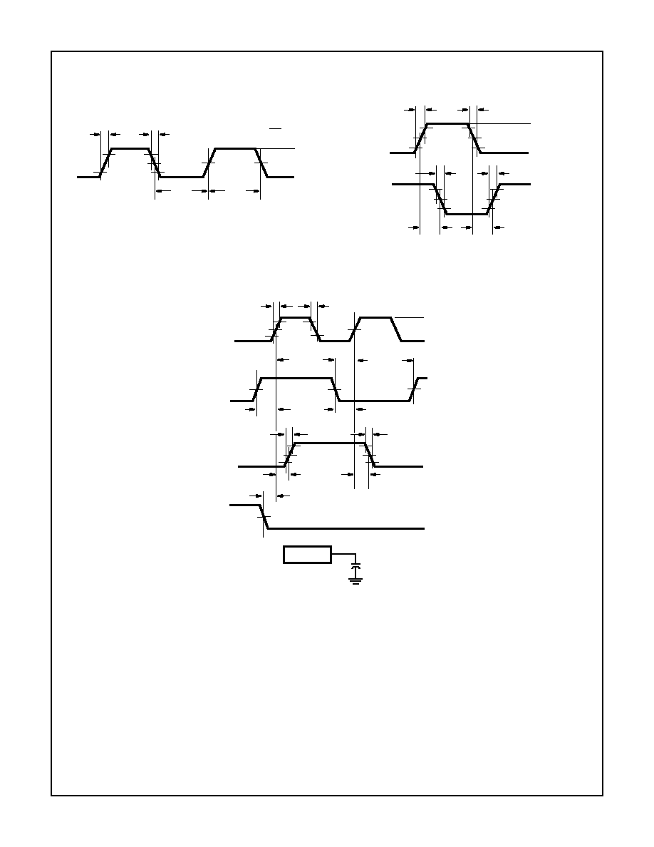
Test Circuits and Waveforms
NOTE: Outputs should be switching from 10% V
CC
to 90% V
CC
in
accordance with device truth table. For f
MAX
, input duty cycle = 50%.
FIGURE 2. HC CLOCK PULSE RISE AND FALL TIMES AND
PULSE WIDTH
FIGURE 3. HC TRANSITION TIMES AND PROPAGATION
DELAY TIMES, COMBINATION LOGIC
FIGURE 4. HC SETUP TIMES, HOLD TIMES, REMOVAL
TIME, AND PROPAGATION DELAY TIMES FOR EDGE
TRIGGERED SEQUENTIAL LOGIC CIRCUITS
CLOCK
90%
50%
10%
GND
V
CC
t
r
C
L
t
f
C
L
50%
50%
t
WL
t
WH
10%
t
WL
+ t
WH
=
fC
L
I
t
PHL
t
PLH
t
THL
t
TLH
90%
50%
10%
50%
10%
INVERTING
OUTPUT
INPUT
GND
V
CC
t
r
= 6ns
t
f
= 6ns
90%
t
r
C
L
t
f
C
L
GND
V
CC
GND
V
CC
50%
90%
10%
GND
CLOCK
INPUT
DATA
INPUT
OUTPUT
SET, RESET
OR PRESET
V
CC
50%
50%
90%
10%
50%
90%
t
REM
t
PLH
t
SU(H)
t
TLH
t
THL
t
H(L)
t
PHL
IC
C
L
50pF
t
SU(L)
t
H(H)
CD54HC4059, CD74HC4059
CD54HC4059, CD74HC4059
PACKAGING INFORMATION
Orderable Device
Status
(1)
Package
Type
Package
Drawing
Pins Package
Qty
Eco Plan
(2)
Lead/Ball Finish
MSL Peak Temp
(3)
5962-8944501JA
ACTIVE
CDIP
J
24
1
TBD
Call TI
Level-NC-NC-NC
CD54HC4059F3A
ACTIVE
CDIP
J
24
1
TBD
Call TI
Level-NC-NC-NC
CD74HC4059E
ACTIVE
PDIP
N
24
15
Pb-Free
(RoHS)
CU NIPDAU
Level-NC-NC-NC
CD74HC4059EE4
ACTIVE
PDIP
N
24
15
Pb-Free
(RoHS)
CU NIPDAU
Level-NC-NC-NC
CD74HC4059M96
ACTIVE
SOIC
DW
24
2000 Green (RoHS &
no Sb/Br)
CU NIPDAU
Level-1-260C-UNLIM
CD74HC4059M96E4
ACTIVE
SOIC
DW
24
2000 Green (RoHS &
no Sb/Br)
CU NIPDAU
Level-1-260C-UNLIM
(1)
The marketing status values are defined as follows:
ACTIVE: Product device recommended for new designs.
LIFEBUY: TI has announced that the device will be discontinued, and a lifetime-buy period is in effect.
NRND: Not recommended for new designs. Device is in production to support existing customers, but TI does not recommend using this part in
a new design.
PREVIEW: Device has been announced but is not in production. Samples may or may not be available.
OBSOLETE: TI has discontinued the production of the device.
(2)
Eco
Plan
-
The
planned
eco-friendly
classification:
Pb-Free
(RoHS)
or
Green
(RoHS
&
no
Sb/Br)
-
please
check
http://www.ti.com/productcontent
for the latest availability information and additional product content details.
TBD: The Pb-Free/Green conversion plan has not been defined.
Pb-Free (RoHS): TI's terms "Lead-Free" or "Pb-Free" mean semiconductor products that are compatible with the current RoHS requirements
for all 6 substances, including the requirement that lead not exceed 0.1% by weight in homogeneous materials. Where designed to be soldered
at high temperatures, TI Pb-Free products are suitable for use in specified lead-free processes.
Green (RoHS & no Sb/Br): TI defines "Green" to mean Pb-Free (RoHS compatible), and free of Bromine (Br) and Antimony (Sb) based flame
retardants (Br or Sb do not exceed 0.1% by weight in homogeneous material)
(3)
MSL, Peak Temp. -- The Moisture Sensitivity Level rating according to the JEDEC industry standard classifications, and peak solder
temperature.
Important Information and Disclaimer:The information provided on this page represents TI's knowledge and belief as of the date that it is
provided. TI bases its knowledge and belief on information provided by third parties, and makes no representation or warranty as to the
accuracy of such information. Efforts are underway to better integrate information from third parties. TI has taken and continues to take
reasonable steps to provide representative and accurate information but may not have conducted destructive testing or chemical analysis on
incoming materials and chemicals. TI and TI suppliers consider certain information to be proprietary, and thus CAS numbers and other limited
information may not be available for release.
In no event shall TI's liability arising out of such information exceed the total purchase price of the TI part(s) at issue in this document sold by TI
to Customer on an annual basis.
PACKAGE OPTION ADDENDUM
www.ti.com
26-Sep-2005
Addendum-Page 1
MECHANICAL DATA
MCDI004A ≠ JANUARY 1995 ≠ REVISED NOVEMBER 1997
POST OFFICE BOX 655303
∑
DALLAS, TEXAS 75265
J (R-GDIP-T**)
CERAMIC DUAL-IN-LINE PACKAGE
24 PINS SHOWN
A
C
0.018 (0,46) MIN
Seating Plane
0.010 (0.25) MAX
Lens Protrusion (Lens Optional)
WIDE
NARR
WIDE
32
NARR
WIDE
0.125 (3,18) MIN
0.514(13,06) 0.571(14,50)
0.541(13,74) 0.598(15,19)
1.668(42,37) 1.668(42,37)
1.632(41,45) 1.632(41,45)
0.590(14,99) 0.590(14,99)
0.624(15,85) 0.624(15,85)
4040084/C 10/97
0.012 (0,30)
0.008 (0,20)
40
0.624(15,85) 0.624(15,85)
0.590(14,99) 0.590(14,99)
2.032(51,61) 2.032(51,61)
2.068(52,53) 2.068(52,53)
0.541(13,74) 0.598(15,19)
0.514(13,06) 0.571(14,50)
B
13
12
0.090 (2,29)
0.060 (1,53)
0.045 (1,14)
0.065 (1,65)
24
1
28
0.022 (0,56)
0.014 (0,36)
NARR
24
NARR
WIDE
0.624(15,85) 0.624(15,85)
0.590(14,99) 0.590(14,99)
1.235(31,37) 1.235(31,37)
1.265(32,13) 1.265(32,13)
0.541(13,74) 0.598(15,19)
0.514(13,06) 0.571(14,50)
"A"
DIM
"B"
"C"
PINS **
MAX
MIN
MIN
MAX
MAX
MIN
0.514(13,06) 0.571(14,50)
0.541(13,74) 0.598(15,19)
1.465(37,21) 1.465(37,21)
1.435(36,45) 1.435(36,45)
0.590(14,99) 0.590(14,99)
0.624(15,85) 0.624(15,85)
0.175 (4,45)
0.140 (3,56)
0.100 (2,54)
NOTES: A. All linear dimensions are in inches (millimeters).
B. This drawing is subject to change without notice.
C. Window (lens) added to this group of packages (24-, 28-, 32-, 40-pin).
D. This package can be hermetically sealed with a ceramic lid using glass frit.
E. Index point is provided on cap for terminal identification.
MECHANICAL DATA
MPDI006B ≠ SEPTEMBER 2001 ≠ REVISED APRIL 2002
POST OFFICE BOX 655303
∑
DALLAS, TEXAS 75265
N (R≠PDIP≠T24)
PLASTIC DUAL≠IN≠LINE
0.020 (0,51) MIN
0.021 (0,53)
0.015 (0,38)
0.100 (2,54)
1
24
0.070 (1,78) MAX
12
13
1.222 (31,04) MAX
0.125 (3,18) MIN
0'≠15'
0.010 (0,25) NOM
0.425 (10,80) MAX
Seating Plane
0.200 (5,08) MAX
0.360 (9,14) MAX
0.010 (0,25)
4040051≠3/D 09/01
NOTES: A. All linear dimensions are in inches (millimeters).
B. This drawing is subject to change without notice.
C. Falls within JEDEC MS≠010
MECHANICAL DATA
MPDI008 ≠ OCTOBER 1994
POST OFFICE BOX 655303
∑
DALLAS, TEXAS 75265
N (R-PDIP-T**)
PLASTIC DUAL-IN-LINE PACKAGE
24 PIN SHOWN
12
Seating Plane
0.560 (14,22)
0.520 (13,21)
13
0.610 (15,49)
0.590 (14,99)
52
48
40
0.125 (3,18) MIN
2.390
(60,71)
(62,23)
(53,09)
(51,82)
2.040
2.090
2.450
2.650
(67,31)
(65,79)
2.590
0.010 (0,25) NOM
4040053 / B 04/95
A
0.060 (1,52) TYP
1
24
32
28
24
1.230
(31,24)
(32,26)
(36,83)
(35,81)
1.410
1.450
1.270
PINS **
DIM
0.015 (0,38)
0.021 (0,53)
A MIN
A MAX
1.650
(41,91)
(40,89)
1.610
0.020 (0,51) MIN
0.200 (5,08) MAX
0.100 (2,54)
M
0.010 (0,25)
0
∞
≠ 15
∞
NOTES: A. All linear dimensions are in inches (millimeters).
B. This drawing is subject to change without notice.
C. Falls within JEDEC MS-011
D. Falls within JEDEC MS-015 (32 pin only)


IMPORTANT NOTICE
Texas Instruments Incorporated and its subsidiaries (TI) reserve the right to make corrections, modifications,
enhancements, improvements, and other changes to its products and services at any time and to discontinue
any product or service without notice. Customers should obtain the latest relevant information before placing
orders and should verify that such information is current and complete. All products are sold subject to TI's terms
and conditions of sale supplied at the time of order acknowledgment.
TI warrants performance of its hardware products to the specifications applicable at the time of sale in
accordance with TI's standard warranty. Testing and other quality control techniques are used to the extent TI
deems necessary to support this warranty. Except where mandated by government requirements, testing of all
parameters of each product is not necessarily performed.
TI assumes no liability for applications assistance or customer product design. Customers are responsible for
their products and applications using TI components. To minimize the risks associated with customer products
and applications, customers should provide adequate design and operating safeguards.
TI does not warrant or represent that any license, either express or implied, is granted under any TI patent right,
copyright, mask work right, or other TI intellectual property right relating to any combination, machine, or process
in which TI products or services are used. Information published by TI regarding third-party products or services
does not constitute a license from TI to use such products or services or a warranty or endorsement thereof.
Use of such information may require a license from a third party under the patents or other intellectual property
of the third party, or a license from TI under the patents or other intellectual property of TI.
Reproduction of information in TI data books or data sheets is permissible only if reproduction is without
alteration and is accompanied by all associated warranties, conditions, limitations, and notices. Reproduction
of this information with alteration is an unfair and deceptive business practice. TI is not responsible or liable for
such altered documentation.
Resale of TI products or services with statements different from or beyond the parameters stated by TI for that
product or service voids all express and any implied warranties for the associated TI product or service and
is an unfair and deceptive business practice. TI is not responsible or liable for any such statements.
Following are URLs where you can obtain information on other Texas Instruments products and application
solutions:
Products
Applications
Amplifiers
amplifier.ti.com
Audio
www.ti.com/audio
Data Converters
dataconverter.ti.com
Automotive
www.ti.com/automotive
DSP
dsp.ti.com
Broadband
www.ti.com/broadband
Interface
interface.ti.com
Digital Control
www.ti.com/digitalcontrol
Logic
logic.ti.com
Military
www.ti.com/military
Power Mgmt
power.ti.com
Optical Networking
www.ti.com/opticalnetwork
Microcontrollers
microcontroller.ti.com
Security
www.ti.com/security
Telephony
www.ti.com/telephony
Video & Imaging
www.ti.com/video
Wireless
www.ti.com/wireless
Mailing Address:
Texas Instruments
Post Office Box 655303 Dallas, Texas 75265
Copyright
2005, Texas Instruments Incorporated