
1
Data sheet acquired from Harris Semiconductor
SCHS207G
Features
∑ Onboard Oscillator
∑ Common Reset
∑ Negative-Edge Clocking
∑ Fanout (Over Temperature Range)
- Standard Outputs . . . . . . . . . . . . . . . 10 LSTTL Loads
- Bus Driver Outputs . . . . . . . . . . . . . 15 LSTTL Loads
∑ Wide Operating Temperature Range . . . -55
o
C to 125
o
C
∑ Balanced Propagation Delay and Transition Times
∑ Significant Power Reduction Compared to LSTTL
Logic ICs
∑ HC Types
- 2V to 6V Operation
- High Noise Immunity: N
IL
= 30%, N
IH
= 30% of V
CC
at V
CC
= 5V
∑ HCT Types
- 4.5V to 5.5V Operation
- Direct LSTTL Input Logic Compatibility,
V
IL
= 0.8V (Max), V
IH
= 2V (Min)
- CMOS Input Compatibility, I
l
1
µ
A at V
OL
, V
OH
Description
The 'HC4060 and 'HCT4060 each consist of an oscillator
section and 14 ripple-carry binary counter stages. The
oscillator configuration allows design of either RC or crystal
oscillator circuits. A Master Reset input is provided which
resets the counter to the all-0's state and disables the
oscillator. A high level on the MR line accomplishes the reset
function. All counter stages are master-slave flip-flops. The
state of the counter is advanced one step in binary order on
the negative transition of
I (and
O). All inputs and outputs
are buffered. Schmitt trigger action on the input-pulse-line
permits unlimited rise and fall times.
In order to achieve a symmetrical waveform in the oscillator
section the HCT4060 input pulse switch points are the same
as in the HC4060; only the MR input in the HCT4060 has
TTL switching levels.
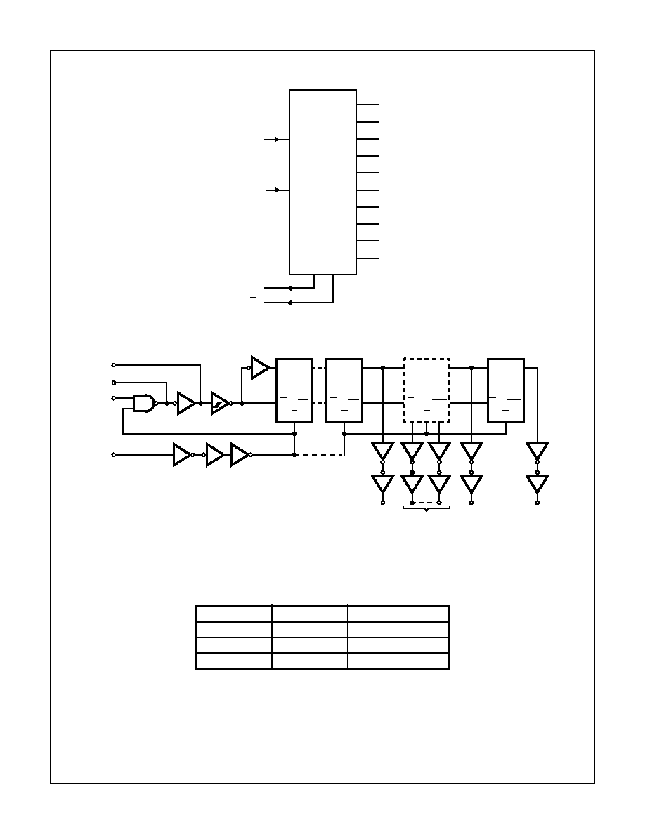
Pinout
CD54HC4060, CD54HCT4060 (CERDIP)
CD74HC4060 (PDIP, SOIC, TSSOP)
CD74HCT4060 (PDIP, SOIC)
TOP VIEW
Ordering Information
PART NUMBER
TEMP. RANGE
(
o
C)
PACKAGE
CD54HC4060F3A
-55 to 125
16 Ld CERDIP
CD54HCT4060F3A
-55 to 125
16 Ld CERDIP
CD74HC4060E
-55 to 125
16 Ld PDIP
CD74HC4060M
-55 to 125
16 Ld SOIC
CD74HC4060MT
-55 to 125
16 Ld SOIC
CD74HC4060M96
-55 to 125
16 Ld SOIC
CD74HC4060PW
-55 to 125
16 Ld TSSOP
CD74HC4060PWR
-55 to 125
16 Ld TSSOP
CD74HC4060PWT
-55 to 125
16 Ld TSSOP
CD74HCT4060E
-55 to 125
16 Ld PDIP
CD74HCT4060M
-55 to 125
16 Ld SOIC
CD74HCT4060MT
-55 to 125
16 Ld SOIC
CD74HCT4060M96
-55 to 125
16 Ld SOIC
NOTE: When ordering, use the entire part number. The suffixes 96
and R denote tape and reel. The suffix T denotes a small-quantity
reel of 250.
14
15
16
9
13
12
11
10
1
2
3
4
5
7
6
8
Q12
Q13
Q14
Q6
Q5
Q7
GND
Q4
V
CC
Q8
Q9
MR
I
O
O
Q10
February 1998 - Revised October 2003
CAUTION: These devices are sensitive to electrostatic discharge. Users should follow proper IC Handling Procedures.
Copyright
©
2003, Texas Instruments Incorporated
CD54HC4060, CD74HC4060,
CD54HCT4060, CD74HCT4060
High-Speed CMOS Logic
14-Stage Binary Counter with Oscillator
[ /Title
(CD74
HC406
0,
CD74
HCT40
60)
/Sub-
ject
(High
Speed
CMOS
2
Functional Diagram
I
Q4
Q5
Q6
Q7
Q9
Q12
Q14
O
O
MR
Q13
Q10
Q8
14-STAGE
RIPPLE
COUNTER
AND
OSCILLATOR
GND = 8
V
CC
= 16
7
5
4
6
13
1
3
2
15
14
12
11
9
10
FIGURE 1. LOGIC BLOCK DIAGRAM
TRUTH TABLE
¯
I
MR
OUTPUT STATE
L
No Change
L
Advance to Next State
X
H
All Outputs are Low
¯
1
Q1
FF1
¯
1
Q1
R
¯
4
Q4
FF4
¯
4
Q4
R
¯
14 Q14
FF14
¯
14 Q14
R
¯
5
Q13
FF5 - FF13
¯
5
Q13
R
7
2
3
5, 4, 6, 14, 13, 15, 1
Q5 - Q10, Q12
MR
12
11
10
9
Q14
Q13
Q4
¯
O
¯
O
¯
1
CD54/74HC4060, CD54/74HCT4060

3
Absolute Maximum Ratings
Thermal Information
DC Supply Voltage, V
CC
. . . . . . . . . . . . . . . . . . . . . . . . -0.5V to 7V
DC Input Diode Current, I
IK
For V
I
< -0.5V or V
I
> V
CC
+ 0.5V
. . . . . . . . . . . . . . . . . . . . . .±
20mA
DC Output Diode Current, I
OK
For V
O
< -0.5V or V
O
> V
CC
+ 0.5V
. . . . . . . . . . . . . . . . . . . .±
20mA
DC Drain Current, per Output, I
O
For -0.5V < V
O
< V
CC
+ 0.5V
. . . . . . . . . . . . . . . . . . . . . . . . . .±
25mA
DC V
CC
or Ground Current, I
CC
. . . . . . . . . . . . . . . . . . . . . . . . .±
50mA
Operating Conditions
Temperature Range, T
A
. . . . . . . . . . . . . . . . . . . . . . -55
o
C to 125
o
C
Supply Voltage Range, V
CC
HC Types . . . . . . . . . . . . . . . . . . . . . . . . . . . . . . . . . . . . .2V to 6V
HCT Types . . . . . . . . . . . . . . . . . . . . . . . . . . . . . . . . .4.5V to 5.5V
DC Input or Output Voltage, V
I
, V
O
. . . . . . . . . . . . . . . . . 0V to V
CC
Input Rise and Fall Time
2V . . . . . . . . . . . . . . . . . . . . . . . . . . . . . . . . . . . . . . 1000ns (Max)
4.5V. . . . . . . . . . . . . . . . . . . . . . . . . . . . . . . . . . . . . . 500ns (Max)
6V . . . . . . . . . . . . . . . . . . . . . . . . . . . . . . . . . . . . . . . 400ns (Max)
Thermal Resistance (Typical, Note 1)
JA
(
o
C/W)
E (PDIP) Package . . . . . . . . . . . . . . . . . . . . . . . . . .
67
M (SOIC) Package. . . . . . . . . . . . . . . . . . . . . . . . . .
73
PW (TSSOP) Package . . . . . . . . . . . . . . . . . . . . . .
108
Maximum Junction Temperature . . . . . . . . . . . . . . . . . . . . . . . 150
o
C
Maximum Storage Temperature Range . . . . . . . . . .-65
o
C to 150
o
C
Maximum Lead Temperature (Soldering 10s) . . . . . . . . . . . . . 300
o
C
(SOIC - Lead Tips Only)
CAUTION: Stresses above those listed in "Absolute Maximum Ratings" may cause permanent damage to the device. This is a stress only rating and operation
of the device at these or any other conditions above those indicated in the operational sections of this specification is not implied.
NOTE:
1. The package thermal impedance is calculated in accordance with JESD 51-7.
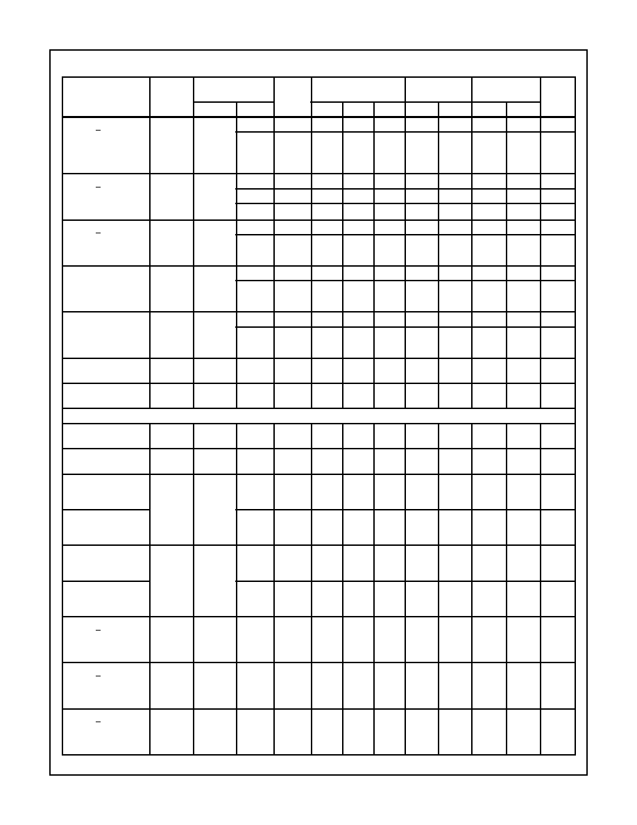
DC Electrical Specifications
PARAMETER
SYMBOL
TEST
CONDITIONS
V
CC
(V)
25
o
C
-40
o
C TO 85
o
C -55
o
C TO 125
o
C
UNITS
V
I
(V)
I
O
(mA)
MIN
TYP
MAX
MIN
MAX
MIN
MAX
HC TYPES
High Level Input
Voltage
V
IH
-
-
2
1.5
-
-
1.5
-
1.5
-
V
4.5
3.15
-
-
3.15
-
3.15
-
V
6
4.2
-
-
4.2
-
4.2
-
V
Low Level Input
Voltage
V
IL
-
-
2
-
-
0.5
-
0.5
-
0.5
V
4.5
-
-
1.35
-
1.35
-
1.35
V
6
-
-
1.8
-
1.8
-
1.8
V
High Level Output
Voltage Q Outputs
CMOS Loads
V
OH
V
IH
or V
IL
-0.02
2
1.9
-
-
1.9
-
1.9
-
V
-0.02
4.5
4.4
-
-
4.4
-
4.4
-
V
-0.02
6
5.9
-
-
5.9
-
5.9
-
V
High Level Output
Voltage Q Outputs
TTL Loads
-
-
-
-
-
-
-
-
-
V
-4
4.5
3.98
-
-
3.84
-
3.7
-
V
-5.2
6
5.48
-
-
5.34
-
5.2
-
V
Low Level Output
Voltage Q Outputs
CMOS Loads
V
OL
V
IH
or V
IL
0.02
2
-
-
0.1
-
0.1
-
0.1
V
0.02
4.5
-
-
0.1
-
0.1
-
0.1
V
0.02
6
-
-
0.1
-
0.1
-
0.1
V
Low Level Output
Voltage Q Outputs
TTL Loads
-
-
-
-
-
-
-
-
-
V
4
4.5
-
-
0.26
-
0.33
-
0.4
V
5.2
6
-
-
0.26
-
0.33
-
0.4
V
High-Level Output
Voltage
O Output
(Pin 10)
CMOS Loads
V
OH
V
CC
or
GND
-0.02
2
1.9
-
-
1.9
-
1.9
-
V
-0.02
4.5
4.4
-
-
4.4
-
4.4
-
V
-0.02
6
5.9
-
-
5.9
-
5.9
-
V
CD54/74HC4060, CD54/74HCT4060
4
High-Level Output
Voltage
O Output
(Pin 10)
TTL Loads
(Note 2)
V
OH
V
CC
or
GND
-2.6
4.5
3.98
-
-
3.84
-
3.7
-
V
-3.3
6
5.48
-
-
5.34
-
5.2
-
V
Low-Level Output
Voltage
O Output
(Pin 10)
CMOS Loads
V
OL
V
CC
or
GND
0.02
2
-
-
0.1
-
0.1
-
0.1
V
0.02
4.5
-
-
0.1
-
0.1
-
0.1
V
0.02
6
-
-
0.1
-
0.1
-
0.1
V
Low-Level Output
Voltage
O Output
(Pin 10)
TTL Loads
V
OL
V
CC
or
GND
2.6
4.5
-
-
0.26
-
0.33
-
0.4
V
3.3
6
-
-
0.26
-
0.33
-
0.4
V
High-Level Output
Voltage
O Output
(Pin 9)
TTL Loads
V
OH
V
IL
or V
IH
-3.2
4.5
3.98
-
-
3.84
-
3.7
-
V
-4.2
6
5.48
-
-
5.34
-
5.2
-
V
Low-Level Output
Voltage
O Output
(Pin 9)
TTL Loads
V
OL
V
IL
or V
IH
-2.6
4.5
-
-
0.26
-
0.33
-
0.4
V
-3.3
6
-
-
0.26
-
0.33
-
0.4
V
Input Leakage
Current
I
I
V
CC
or
GND
-
6
-
-
±
0.1
-
±
1
-
±
1
µ
A
Quiescent Device
Current
I
CC
V
CC
or
GND
0
6
-
-
8
-
80
-
160
µ
A
HCT TYPES
High Level Input
Voltage
V
IH
-
-
4.5 to
5.5
2
-
-
2
-
2
-
V
Low Level Input
Voltage
V
IL
-
-
4.5 to
5.5
-
-
0.8
-
0.8
-
0.8
V
High Level Output
Voltage Q Outputs
CMOS Loads
V
OH
V
IH
or V
IL
(Note 3)
-0.02
4.5
4.4
-
-
4.4
-
4.4
-
V
High Level Output
Voltage Q Outputs
TTL Loads
-4
4.5
3.98
-
-
3.84
-
3.7
-
V
Low Level Output
Voltage Q Outputs
CMOS Loads
V
OL
V
IH
or V
IL
(Note 3)
0.02
4.5
-
-
0.1
-
0.1
-
0.1
V
Low Level Output
Voltage Q Outputs
TTL Loads
4
4.5
-
-
0.26
-
0.33
-
0.4
V
High-Level Output
Voltage
O Output
(Pin 10)
CMOS Loads
V
OH
V
CC
or
GND
-0.02
4.5
4.4
-
-
4.4
-
4.4
-
V
High-Level Output
Voltage
O Output
(Pin 10)
TTL Loads (Note 2)
V
OH
V
CC
or
GND
-2.6
4.5
3.98
-
-
3.84
-
3.7
-
V
Low-Level Output
Voltage
O Output
(Pin 10)
CMOS Loads
V
OL
V
CC
or
GND
0.02
4.5
-
-
0.1
-
0.1
-
0.1
V
DC Electrical Specifications
(Continued)
PARAMETER
SYMBOL
TEST
CONDITIONS
V
CC
(V)
25
o
C
-40
o
C TO 85
o
C -55
o
C TO 125
o
C
UNITS
V
I
(V)
I
O
(mA)
MIN
TYP
MAX
MIN
MAX
MIN
MAX
CD54/74HC4060, CD54/74HCT4060

5
Low-Level Output
Voltage
O Output
(Pin 10)
TTL Loads
V
OL
V
CC
or
GND
2.6
4.5
-
-
0.26
-
0.33
-
0.4
V
High-Level Output
Voltage
O Output
(Pin 9)
TTL Loads
V
OH
V
IL
or V
IH
-3.2
4.5
3.98
-
-
3.84
-
3.7
-
V
Low-Level Output
Voltage
O Output
(Pin 9)
TTL Loads
V
OL
V
IH
or V
IL
(Note 3)
3.2
4.5
-
0.26
-
0.33
-
0.4
V
Input Leakage
Current
I
I
Any
Voltage
Between
V
CC
and
GND
-
5.5
-
±
0.1
-
±
1
-
±
1
µ
A
Quiescent Device
Current
I
CC
V
CC
or
GND
0
5.5
-
-
8
-
80
-
160
µ
A
Additional Quiescent
Device Current Per
Input Pin: 1 Unit Load
I
CC
(Note 4)
V
CC
- 2.1
-
4.5 to
5.5
-
100
360
-
450
-
490
µ
A
NOTES:
2. Limits not valid when pin 12 (instead of pin 11) is used as control input.
3. For pin 11 V
IH
= 3.15V, V
IL
= 0.9V.
4. For dual-supply systems theoretical worst case (V
I
= 2.4V, V
CC
= 5.5V) specification is 1.8mA.
DC Electrical Specifications
(Continued)
PARAMETER
SYMBOL
TEST
CONDITIONS
V
CC
(V)
25
o
C
-40
o
C TO 85
o
C -55
o
C TO 125
o
C
UNITS
V
I
(V)
I
O
(mA)
MIN
TYP
MAX
MIN
MAX
MIN
MAX
HCT Input Loading Table
INPUT
UNIT LOADS
MR
0.35
NOTE: Unit Load is
I
CC
limit specified in DC Electrical Specifica-
tions Table, e.g. 360
µ
A max at 25
o
C.
Prerequisite for Switching Specifications
PARAMETER
SYMBOL
V
CC
(V)
25
o
C
-40
o
C TO 85
o
C
-55
o
C TO 125
o
C
UNITS
MIN
TYP
MAX
MIN
TYP
MAX
MIN
TYP
MAX
HC TYPES
Maximum Input Pulse
Frequency
f
max
2
6
-
-
5
-
-
4
-
-
MHz
4.5
30
-
-
25
-
-
20
-
-
MHz
6
35
-
-
29
-
-
23
-
-
MHz
Input Pulse Width
t
W
2
80
-
-
100
-
-
120
-
-
ns
4.5
16
-
-
20
-
-
24
-
-
ns
6
14
-
-
17
-
-
20
-
-
ns
Reset Removal Time
t
REM
2
100
-
-
125
-
-
150
-
-
ns
4.5
20
-
-
25
-
-
30
-
-
ns
6
17
-
-
21
-
-
26
-
-
ns
CD54/74HC4060, CD54/74HCT4060