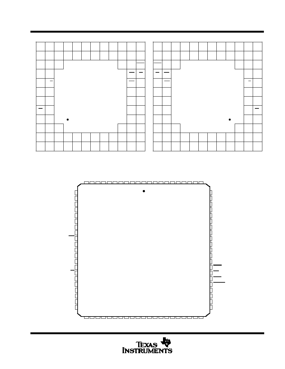
TLC34058
256
×
24 COLOR PALETTE
SLAS050 D3961, NOVEMBER 1991
POST OFFICE BOX 655303
·
DALLAS, TEXAS 75265
Copyright
©
1991, Texas Instruments Incorporated
1
·
LinEPIC
TM
1-
µ
m CMOS Process
·
125-MHz Pipelined Architecture
·
Available Clock Rates . . . 80, 110, 125,
135 MHz
·
Dual-Port Color RAM
256 Words x 24 Bits
·
Bit Plane Read and Blink Masks
·
EIA RS-343-A Compatible Outputs
·
Functionally Interchangeable With
Brooktree
®
Bt458
·
Direct Interface to TMS340XX Graphics
Processors
·
Standard Microprocessor Unit (MPU)
Palette Interface
·
Multiplexed TTL Pixel Ports
·
Triple Digital-to-Analog Converters (DACs)
·
Dual-Port Overlay Registers . . . 4
×
24 Bits
·
5-V Power Supply
description
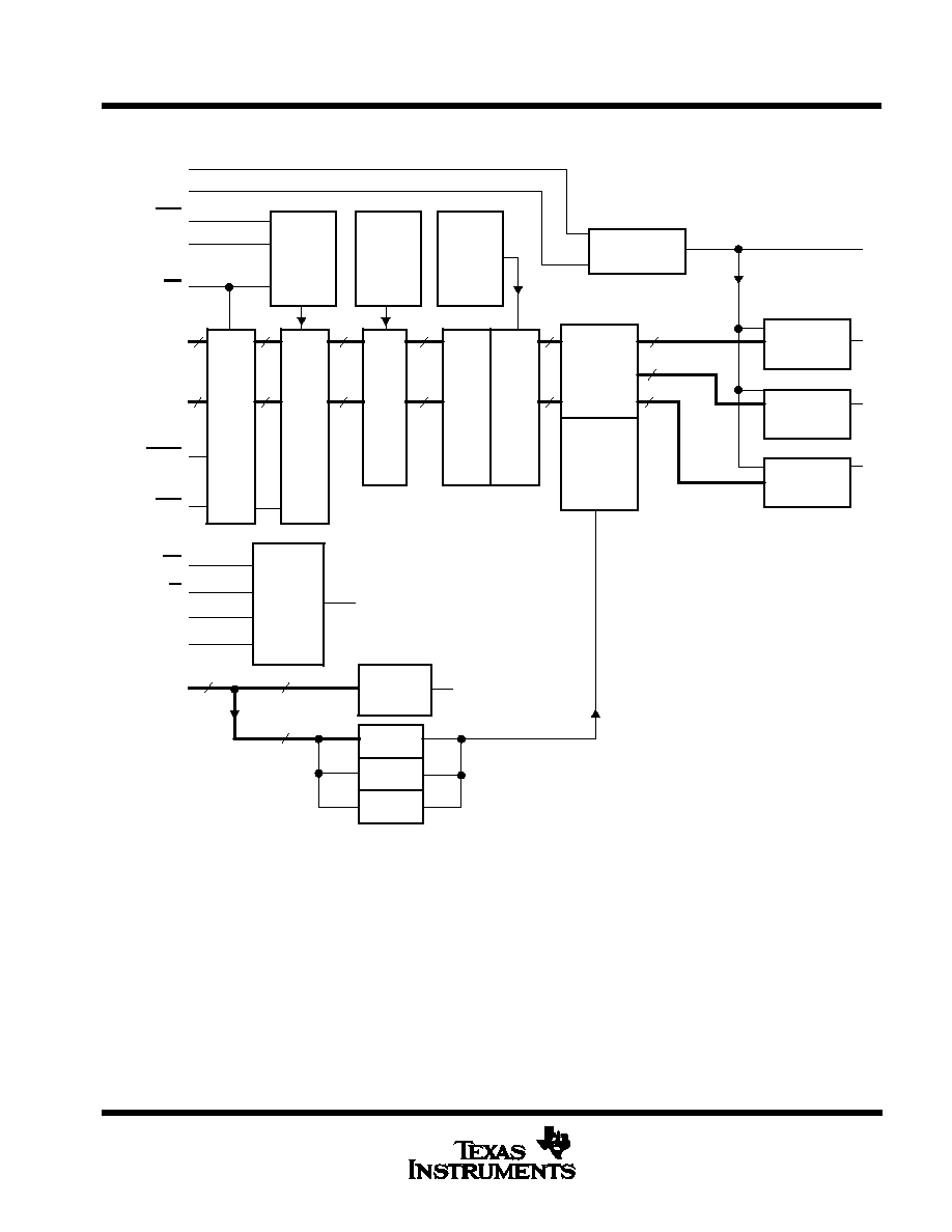
The TLC34058 color-palette integrated circuit is specifically developed for high-resolution color graphics in such
applications as CAE/CAD/CAM, image processing, and video reconstruction.
The architecture provides for the display of 1280
×
1024 bit-mapped color graphics (up to 8 bits per pixel
resolution) with 2 bits of overlay information. The TLC34058 has a 256-word
×
24-bit RAM used as a lookup
table with three 8-bit video D/A converters.
On-chip features such as high-speed pixel clock logic minimize costly ECL interface. Multiple pixel ports and
internal multiplexing provide TTL-compatible interface (up to 32 MHz) to the frame buffer while maintaining
sophisticated color graphic data rates (up to 135 MHz). Programmable blink rates, bit plane masking and
blinking, color overlay capability, and a dual-port palette RAM are other key features. The TLC34058 generates
red, green, and blue signals compatible with EIA RS-343-A and can drive, without external buffering, 75-
coaxial cables terminated at each end.
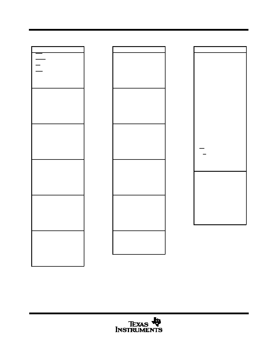
AVAILABLE OPTIONS
TA
SPEED
DAC
PACKAGE
TA
SPEED
RESOLUTION
Ceramic Grid Array (GA)
Plastic Chip Carrier (FN)
80 MHz
8 Bits
TLC34058-80GA
TLC34058-80FN
0
°
C
To
110 MHz
8 Bits
TLC34058-110GA
TLC34058-110FN
To
70
°
C
125 MHz
8 Bits
TLC34058-125GA
TLC34058-125FN
70 C
135 MHz
8 Bits
TLC34058-135GA
TLC34058-135FN
LinEPIC is a trademark of Texas Instruments Incorporated.
Brooktree
®
is a registered trademark of Brooktree Corporation.
PRODUCTION DATA information is current as of publication date.
Products conform to specifications per the terms of Texas Instruments
standard warranty. Production processing does not necessarily include
testing of all parameters.
TLC34058
256
×
24 COLOR PALETTE
SLAS050 D3961, NOVEMBER 1991
POST OFFICE BOX 655303
·
DALLAS, TEXAS 75265
5
Terminal Functions
PIN NAME
I/O
DESCRIPTION
BLK
I
Composite blank control. This TTL-compatible blanking input is stored in the input latch on the rising edge of LD. When
BLK
g
g
g
low, BLK drives the DAC outputs to the blanking level, as shown in Table 6. This causes the P0 P7 [A E] and
g
OL0 OL1 [A E] inputs to be ignored. When high, BLK allows the device to perform in the standard manner.
C0, C1
I
Command control inputs. The inputs specify the type of write or read operation (see Tables 1, 2, 3, and 4). These
y
y
(
)
TTL-compatible inputs are latched on the falling edge of CE.
CE
I
Chip enable. This TTL-compatible input control allows data to be stored and enables data to be written or read (see
CE
(
Figure 1). When low, CE enables data to be written or read. When high, CE allows data to be internally latched on the
g
g
rising edge during write operations. Care should be taken to avoid transients on this input.
CLK
I
Clock. This input provides the pixel clock rate. CLK and CLK inputs are designed to be driven by ECL logic using a 5-V
g
y
g
g
single supply.
CLK
I
Clock. This input is the complement of CLK and also provides the pixel clock rate.
COMP
I
Compensation. This input is used to compensate the internal reference amplifier (see the video generation section).
(
g
)
A 0.1-
µ
F ceramic capacitor is connected between this pin and VDD (see Figure 4). The highest possible supply voltage
µ
DD
g
g
g
rejection ratio is attained by connecting the capacitor to VDD rather than to GND.
D0 D7
I
Data input bus. This TTL-compatible bus transfers data into or out of the device. The data bus is an 8-bit bidirectional
bus where D0 is the least significant bit.
FS ADJ
I
Full-scale adjust control. A resistor Rset, (see Figure 4) which is connected between this pin and GND, controls the
j
set, (
g
)
,
magnitude of the full-scale video signal. Note that the proportional current and voltage relationships in Figure 3 are
g
g
g
g
maintained independent of the full-scale output current. The relationships between Rset and the IOR, IOG, and IOB
full-scale output currents are:
R
(
)
11294
V
(V) / IOG( A)
Rset(
) = 11294
×
Vref(V) / IOG(mA)
IOR IOB (mA)
8067
×
V
(V) / R
(
)
IOR, IOB (mA) = 8067
×
Vref(V) / Rset(
)
GND
Ground. All GND pins must be connected together.
IOR, IOG
O
Current outputs, red, green, and blue. High-impedance red, green, and blue video analog current outputs can directly
IOB
g
g
g
g
y
drive a 75-
coaxial terminated at each end (see Figure 4).
LD
I
Load control. This TTL-compatible load control input latches the P0 P7 [A E], OL0 OL1 [A E], BLK, and SYNC
[
],
[
],
,
inputs on its rising edge. The LD strobe occurs at 1/4 or 1/5 the clock rate and may be phase independent of the CLK
and CLK inputs. The LD duty cycle limits are specified in the timing requirements table.
OL0A OL1A
l
Overlay selection inputs. These TTL-compatible selection inputs for the Palette overlay registers are stored in the input
OL0A OL1A
OL0B OL1B
l
Overlay selection in uts. These TTL com atible selection in uts for the Palette overlay registers are stored in the in ut
latch on the rising edge of LD. These inputs (up to 2 bits per pixel), along with bit CR6 of the command register (refer
OL0B OL1B
OL0C OL1C
latch on the rising edge of LD. These in uts (u to 2 bits er ixel), along with bit CR6 of the command register (refer
to the command register section and Table 5), specify whether the color information is selected from the palette RAM
O 0C O
C
OL0D OL1D
to t e co
a d eg ste sect o a d ab e 5), s ec y
et e t e co o
o
at o
s se ected o
t e a ette
or the overlay registers. If the color information is selected from the overlay registers, the OL0 OL1 [A E] inputs
OL0E OL1E
y
g
y
g
,
[
]
address a particular overlay register. The OL0 OL1 [A D] or OL0 OL1 [A E] inputs are simultaneously input to the
y
g
[
]
[
]
y
device (see the description of bit CR7 in the command register section). The OL0 OL1 [A] inputs are processed first,
(
g
)
[ ]
,
then the OL0 OL1 [B] inputs, and so on. When obtaining the color information from the overlay registers, the P0 P7
[ ]
,
g
y
g
,
[A E] inputs are ignored. Unused inputs should be connected to GND.
P0A P7A
l
Address inputs. These TTL-compatible address inputs for the Palette RAM are stored in the input latch on the rising edge
P0B P7B
g
g
of LD. These address inputs (up to 8-bits per pixel) select one of 256 24-bit words in the palette RAM, which is
P0C P7C
subsequently input to the red, green, and blue D/A converters as three 8-bit or 4-bit bytes. Four or five addresses are
P0D P7D
P0E P7E
simultaneously input to the P0 P7 [A D] or P0 P7 [A E] ports, respectively (see the description of bit CR7 in the
d
i t
ti
) Th
d dd
d b P0A P7A i fi t
t t th DAC
th
th
d dd
d b
P0E P7E
command register section). The word addressed by P0A P7A is first sent to the DACs, then the word addressed by
P0B P7B and so on Unused inputs should be connected to GND
P0B P7B, and so on. Unused inputs should be connected to GND.
REF
I
Reference voltage. 1.235-V is supplied at this input. An external voltage reference circuit, shown in Figure 4, is sug-
g
g
,
g
,
g
gested. Generating the reference voltage with a resistor network is not recommended since low-frequency power supply
g
g
g
noisewill directly couple into the DAC output signals. This input must be decoupled by connecting a 0.1-
µ
F ceramic
capacitorbetween VREF and GND.