"9-Bit Bus-Interface Flip-Flops With 3-State Outputs"
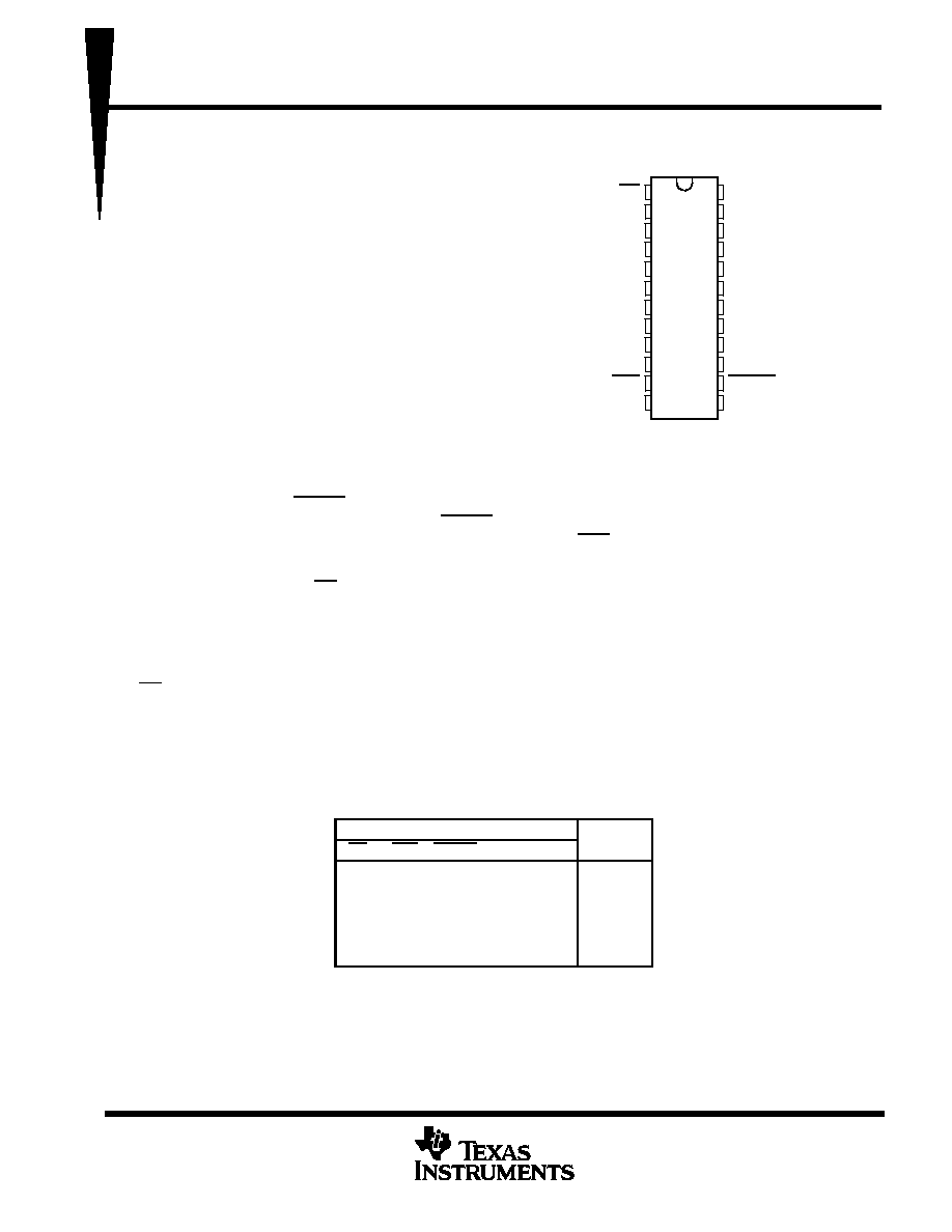
SN54ALS29823 . . . JT PACKAGE
SN74ALS29823 . . . DW OR NT PACKAGE
(TOP VIEW)
1
2
3
4
5
6
7
8
9
10
11
12
24
23
22
21
20
19
18
17
16
15
14
13
OE
1D
2D
3D
4D
5D
6D
7D
8D
9D
CLR
GND
V
CC
1Q
2Q
3Q
4Q
5Q
6Q
7Q
8Q
9Q
CLKEN
CLK
SN54ALS29823, SN74ALS29823
9-BIT BUS-INTERFACE FLIP-FLOPS
WITH 3-STATE OUTPUTS
SDAS146B JANUARY 1986 REVISED JANUARY 1995
Copyright
©
1995, Texas Instruments Incorporated
1
POST OFFICE BOX 655303
·
DALLAS, TEXAS 75265
·
Functionally Equivalent to AMD's AM29823
·
Provide Extra Data Width Necessary for
Wider Address/Data Paths or Buses With
Parity
·
Outputs Have Undershoot-Protection
Circuitry
·
Power-Up High-Impedance State
·
Buffered Control Inputs Reduce dc Loading
Effects
·
Package Options Include Plastic
Small-Outline (DW) Packages and Standard
Plastic (NT) and Ceramic (JT) 300-mil DIPs
description
These 9-bit flip-flops feature 3-state outputs
designed specifically for driving highly capacitive
or relatively low-impedance loads. They are particularly suitable for implementing wider buffer registers, I/O
ports, bidirectional bus drivers, parity bus interfacing, and working registers.
With the clock-enable (CLKEN) input low, the nine D-type edge-triggered flip-flops enter data on the low-to-high
transitions of the clock (CLK) input. Taking CLKEN high disables the clock buffer, latching the outputs. The
ALS29823 have noninverting data (D) inputs. Taking the clear (CLR) input low causes the nine Q outputs to
go low independently of the clock.
A buffered output-enable (OE) input places the nine outputs in either a normal logic state (high or low logic levels)
or a high-impedance state. The outputs also are in the high-impedance state during power-up and power-down
conditions. The outputs remain in the high-impedance state while the device is powered down. In the
high-impedance state, the outputs neither load nor drive the bus lines significantly. The high-impedance state
and increased drive provide the capability to drive bus lines without interface or pullup components.
OE does not affect the internal operation of the flip-flops. Old data can be retained or new data can be entered
while the outputs are in the high-impedance state.
The SN54ALS29823 is characterized for operation over the full military temperature range of 55
°
C to 125
°
C.
The SN74ALS29823 is characterized for operation from 0
°
C to 70
°
C.
FUNCTION TABLE
(each flip-flop)
INPUTS
OUTPUT
OE
CLR
CLKEN
CLK
D
Q
L
L
X
X
X
L
L
H
L
H
H
L
H
L
L
L
L
H
H
X
X
Q0
H
X
X
X
X
Z
PRODUCTION DATA information is current as of publication date.
Products conform to specifications per the terms of Texas Instruments
standard warranty. Production processing does not necessarily include
testing of all parameters.
SN54ALS29823, SN74ALS29823
9-BIT BUS-INTERFACE FLIP-FLOPS
WITH 3-STATE OUTPUTS
SDAS146B JANUARY 1986 REVISED JANUARY 1995
2
POST OFFICE BOX 655303
·
DALLAS, TEXAS 75265
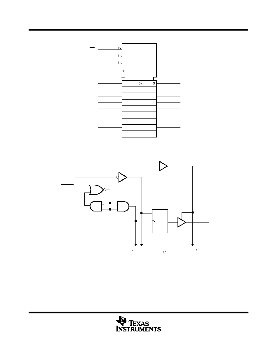
logic symbol
EN
1
7
6D
8
7D
9
8D
10
9D
2D
2
1D
6Q
18
7Q
17
8Q
16
9Q
15
1Q
23
3
2D
4
3D
5
4D
6
5D
2Q
22
3Q
21
4Q
20
5Q
19
OE
13
CLK
1C2
R
11
CLR
G1
14
CLKEN
This symbol is in accordance with ANSI/IEEE Std 91-1984 and IEC Publication 617-12.
logic diagram (positive logic)
To Eight Other Channels
23
2
1
1D
1Q
R
C1
1D
CLKEN
CLK
11
14
13
OE
CLR
SN54ALS29823, SN74ALS29823
9-BIT BUS-INTERFACE FLIP-FLOPS
WITH 3-STATE OUTPUTS
SDAS146B JANUARY 1986 REVISED JANUARY 1995
3
POST OFFICE BOX 655303
·
DALLAS, TEXAS 75265
absolute maximum ratings over operating free-air temperature range (unless otherwise noted)
Supply voltage, V
CC
7 V
. . . . . . . . . . . . . . . . . . . . . . . . . . . . . . . . . . . . . . . . . . . . . . . . . . . . . . . . . . . . . . . . . . . . . . . .
Input voltage, V
I
5.5 V
. . . . . . . . . . . . . . . . . . . . . . . . . . . . . . . . . . . . . . . . . . . . . . . . . . . . . . . . . . . . . . . . . . . . . . . . . .
Voltage applied to a disabled high-impedance output
5.5 V
. . . . . . . . . . . . . . . . . . . . . . . . . . . . . . . . . . . . . . . . . .
Operating free-air temperature range, T
A
: SN54ALS29823
55
°
C to 125
°
C
. . . . . . . . . . . . . . . . . . . . . . . . . . .
Storage temperature range
65
°
C to 150
°
C
. . . . . . . . . . . . . . . . . . . . . . . . . . . . . . . . . . . . . . . . . . . . . . . . . . . . . . .
Stresses beyond those listed under "absolute maximum ratings" may cause permanent damage to the device. These are stress ratings only, and
functional operation of the device at these or any other conditions beyond those indicated under "recommended operating conditions" is not
implied. Exposure to absolute-maximum-rated conditions for extended periods may affect device reliability.
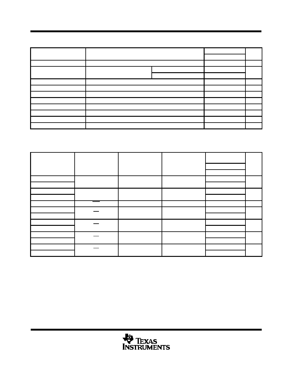
recommended operating conditions
SN54ALS29823
UNIT
MIN
NOM
MAX
UNIT
VCC
Supply voltage
4.5
5
5.5
V
VIH
High-level input voltage
2
V
VIL
Low-level input voltage
0.8
V
IOH
High-level output current
18
mA
IOL
Low-level output current
32
mA
t
Pulse duration
CLR low
7
ns
tw
Pulse duration
CLK high or low
8
ns
CLR inactive
7
tsu
Setup time before CLK
Data
4
ns
CLKEN high or low
8
th
Hold time after CLK
CLKEN
2
ns
th
Hold time after CLK
Data
4
ns
TA
Operating free-air temperature
55
25
125
°
C
electrical characteristics over recommended operating free-air temperature range (unless
otherwise noted)
PARAMETER
TEST CONDITIONS
SN54ALS29823
UNIT
PARAMETER
TEST CONDITIONS
MIN
TYP
MAX
UNIT
VIK
VCC = 4.5 V,
II = 18 mA
1.2
V
VOH
VCC = 4 5 V
IOH = 12 mA
2.4
3.3
V
VOH
VCC = 4.5 V
IOH = 18 mA
2
V
VOL
VCC = 4.5 V,
IOL = 32 mA
0.25
0.5
V
IOZH
VCC = 5.5 V,
VO = 2.4 V
50
µ
A
IOZL
VCC = 5.5 V,
VO = 0.4 V
50
µ
A
II
VCC = 5.5 V,
VI = 5.5 V
0.1
mA
IIH
VCC = 5.5 V,
VI = 2.7 V
20
µ
A
IIL
VCC = 5.5 V,
VI = 0.4 V
0.5
mA
IOS§
VCC = 5.5 V,
VO = 0
75
250
mA
Outputs high
90
ICC
VCC = 5.5 V
Outputs low
105
mA
Outputs open
115
All typical values are at VCC = 5 V, TA = 25
°
C.
§ Not more than one output should be shorted at a time, and the duration of the short circuit should not exceed one second.
SN54ALS29823, SN74ALS29823
9-BIT BUS-INTERFACE FLIP-FLOPS
WITH 3-STATE OUTPUTS
SDAS146B JANUARY 1986 REVISED JANUARY 1995
4
POST OFFICE BOX 655303
·
DALLAS, TEXAS 75265
switching characteristics (see Figure 1)
PARAMETER
FROM
TO
TEST CONDITIONS
VCC = MIN to MAX,
TA = MIN to MAX
UNIT
PARAMETER
FROM
(INPUT)
TO
(OUTPUT)
TEST CONDITIONS
SN54ALS29823
UNIT
MIN
MAX
tPLH
CLK
An Q
C
50 pF
2
11.5
ns
tPHL
CLK
Any Q
CL = 50 pF
2
11.5
ns
tPLH
CLK
An Q
C
300 pF
2
21
ns
tPHL
CLK
Any Q
CL = 300 pF
2
21
ns
tPHL
CLR
Any Q
CL = 50 pF
1
17.5
ns
tPZH
OE
An Q
C
50 pF
1
17
ns
tPZL
OE
Any Q
CL = 50 pF
1
17
ns
tPZH
OE
An Q
C
300 pF
1
25
ns
tPZL
OE
Any Q
CL = 300 pF
1
29.5
ns
tPHZ
OE
An Q
C
50 pF
1
16
ns
tPLZ
OE
Any Q
CL = 50 pF
1
14
ns
tPHZ
OE
Any Q
CL 5 pF
1
12
ns
tPLZ
OE
Any Q
CL = 5 pF
1
11
ns
For conditions shown as MIN or MAX, use the appropriate value specified under recommended operating conditions.
absolute maximum ratings over operating free-air temperature range (unless otherwise noted)
Supply voltage, V
CC
7 V
. . . . . . . . . . . . . . . . . . . . . . . . . . . . . . . . . . . . . . . . . . . . . . . . . . . . . . . . . . . . . . . . . . . . . . . .
Input voltage, V
I
5.5 V
. . . . . . . . . . . . . . . . . . . . . . . . . . . . . . . . . . . . . . . . . . . . . . . . . . . . . . . . . . . . . . . . . . . . . . . . . .
Voltage applied to a disabled 3-state output
5.5 V
. . . . . . . . . . . . . . . . . . . . . . . . . . . . . . . . . . . . . . . . . . . . . . . . . .
Operating free-air temperature range, T
A
: SN74ALS29823
0
°
C to 70
°
C
. . . . . . . . . . . . . . . . . . . . . . . . . . . . . . .
Storage temperature range
65
°
C to 150
°
C
. . . . . . . . . . . . . . . . . . . . . . . . . . . . . . . . . . . . . . . . . . . . . . . . . . . . . . .
Stresses beyond those listed under "absolute maximum ratings" may cause permanent damage to the device. These are stress ratings only, and
functional operation of the device at these or any other conditions beyond those indicated under "recommended operating conditions" is not
implied. Exposure to absolute-maximum-rated conditions for extended periods may affect device reliability.
recommended operating conditions
SN74ALS29823
UNIT
MIN
NOM
MAX
UNIT
VCC
Supply voltage
4.75
5
5.25
V
VIH
High-level input voltage
2
V
VIL
Low-level input voltage
0.8
V
IOH
High-level output current
24
mA
IOL
Low-level output current
48
mA
t
Pulse duration
CLR low
5
ns
tw
Pulse duration
CLK high or low
5
ns
CLR inactive
5
tsu
Setup time before CLK
Data
2
ns
CLKEN high or low
6
th
Hold time after CLK
CLKEN
0
ns
th
Hold time after CLK
Data
2
ns
TA
Operating free-air temperature
0
25
70
°
C
SN54ALS29823, SN74ALS29823
9-BIT BUS-INTERFACE FLIP-FLOPS
WITH 3-STATE OUTPUTS
SDAS146B JANUARY 1986 REVISED JANUARY 1995
5
POST OFFICE BOX 655303
·
DALLAS, TEXAS 75265
electrical characteristics over recommended operating free-air temperature range (unless
otherwise noted)
PARAMETER
TEST CONDITIONS
SN74ALS29823
UNIT
PARAMETER
TEST CONDITIONS
MIN
TYP
MAX
UNIT
VIK
VCC = 4.75 V,
II = 18 mA
1.2
V
VOH
VCC = 4 75 V
IOH = 15 mA
2.4
3.3
V
VOH
VCC = 4.75 V
IOH = 24 mA
2
3.1
V
VOL
VCC = 4.75 V,
IOL = 48 mA
0.35
0.5
V
IOZH
VCC = 5.25 V,
VO = 2.4 V
20
µ
A
IOZL
VCC = 5.25 V,
VO = 0.4 V
20
µ
A
II
VCC = 5.25 V,
VI = 5.5 V
0.1
mA
IIH
VCC = 5.25 V,
VI = 2.7 V
20
µ
A
IIL
VCC = 5.25 V,
VI = 0.4 V
0.2
mA
IOS
VCC = 5.25 V,
VO = 0
75
250
mA
ICC
VCC = 5.25 V,
Outputs open
80
115
mA
All typical values are at VCC = 5 V, TA = 25
°
C.
Not more than one output should be shorted at a time, and the duration of the short circuit should not exceed one second.
switching characteristics (see Figure 1)
PARAMETER
FROM
TO
TEST CONDITIONS
VCC = MIN to MAX§,
TA = MIN to MAX§
UNIT
PARAMETER
FROM
(INPUT)
TO
(OUTPUT)
TEST CONDITIONS
SN74ALS29823
UNIT
MIN
MAX
tPLH
CLK
An Q
C
50 pF
2
10
ns
tPHL
CLK
Any Q
CL = 50 pF
2
10
ns
tPLH
CLK
An Q
C
300 pF
16
ns
tPHL
CLK
Any Q
CL = 300 pF
16
ns
tPHL
CLR
Any Q
CL = 50 pF
12
ns
tPZH
OE
An Q
C
50 pF
14
ns
tPZL
OE
Any Q
CL = 50 pF
14
ns
tPZH
OE
An Q
C
300 pF
20
ns
tPZL
OE
Any Q
CL = 300 pF
23
ns
tPHZ
OE
An Q
C
50 pF
14
ns
tPLZ
OE
Any Q
CL = 50 pF
12
ns
tPHZ
OE
Any Q
CL 5 pF
9
ns
tPLZ
OE
Any Q
CL = 5 pF
9
ns
§ For conditions shown as MIN or MAX, use the appropriate value specified under recommended operating conditions.