SN55LBC175
QUADRUPLE LOW-POWER DIFFERENTIAL LINE RECEIVER
SGLS083A ≠ MARCH 1995 ≠ REVISED JUNE 2000
1
POST OFFICE BOX 655303
∑
DALLAS, TEXAS 75265
D
Meets EIA Standards RS-422-A, RS-423-A,
RS-485, and CCITT V.11
D
Designed to Operate With Pulse Durations
as Short as 20 ns
D
Designed for Multipoint Transmission on
Long Bus Lines in Noisy Environments
D
Input Sensitivity . . .
±
200 mV
D
Low-Power Consumption . . . 20 mA Max
D
Open-Circuit Fail-Safe Design
D
Common-Mode Input Voltage Range of
≠ 7 V to 12 V
description
The SN55LBC175 is a monolithic quadruple
differential line receiver with 3-state outputs and is
designed to meet the requirements of the EIA
Standards RS-422-A, RS-423-A, RS-485, and
CCITT V.11. This device is optimized for balanced
multipoint bus transmission at data rates up to and
exceeding 10 million bits per second. The
receivers are enabled in pairs with an active-high
enable input. Each differential receiver input
features high impedance, hysteresis for
increased noise immunity, and sensitivity of
±
200
mV over a common-mode input voltage range of
12 V to ≠7 V. Fail-safe design ensures that if the
inputs are open-circuited, the outputs are always
high. This device is designed using the Texas
Instruments proprietary LinBiCMOS
TM
technology
allowing low power consumption, high switching
speeds, and robustness.
This device offers optimum performance when used with the SN55LBC174 quadruple line driver. The
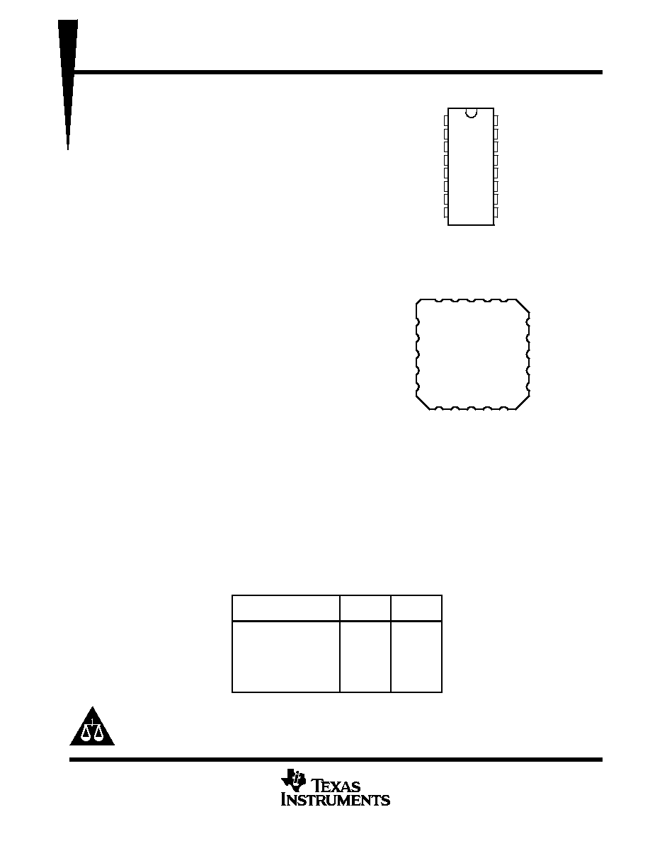
SN55LBC175 is available in the 16-pin CDIP (J) package, a 16-pin CPAK (W) package, or a 20-pin LCCC (FK)
package.
The SN55LBC175 is characterized over the military temperature range of ≠ 55
∞
C to 125
∞
C.
FUNCTION TABLE
(each receiver)
DIFFERENTIAL INPUTS
A ≠ B
ENABLE
OUTPUT
Y
VID
0.2 V
H
H
≠ 0.2 V < VID < 0.2 V
H
?
VID
≠ 0.2 V
H
L
X
L
Z
Open circuit
H
H
H = high level, L = low level, X = irrelevant,
Z = high impedance (off), ? = indeterminate
Copyright
©
2000, Texas Instruments Incorporated
PRODUCTION DATA information is current as of publication date.
Products conform to specifications per the terms of Texas Instruments
standard warranty. Production processing does not necessarily include
testing of all parameters.
Please be aware that an important notice concerning availability, standard warranty, and use in critical applications of
Texas Instruments semiconductor products and disclaimers thereto appears at the end of this data sheet.
LinBiCMOS is a trademark of Texas Instruments.
1
2
3
4
5
6
7
8
16
15
14
13
12
11
10
9
1B
1A
1Y
1, 2EN
2Y
2A
2B
GND
V
CC
4B
4A
4Y
3, 4EN
3Y
3A
3B
J OR W PACKAGE
(TOP VIEW)
NC ≠ No internal connection
FK PACKAGE
(TOP VIEW)
19
20
1
3
2
17
18
16
15
14
13
12
11
9
10
5
4
6
7
8
4A
4Y
NC
3, 4EN
3Y
1Y
1, 2EN
NC
2Y
2A
1A
1B
NC
4B
GND
NC
3B
3A
2B
V
CC
SN55LBC175
QUADRUPLE LOW-POWER DIFFERENTIAL LINE RECEIVER
SGLS083A ≠ MARCH 1995 ≠ REVISED JUNE 2000
2
POST OFFICE BOX 655303
∑
DALLAS, TEXAS 75265
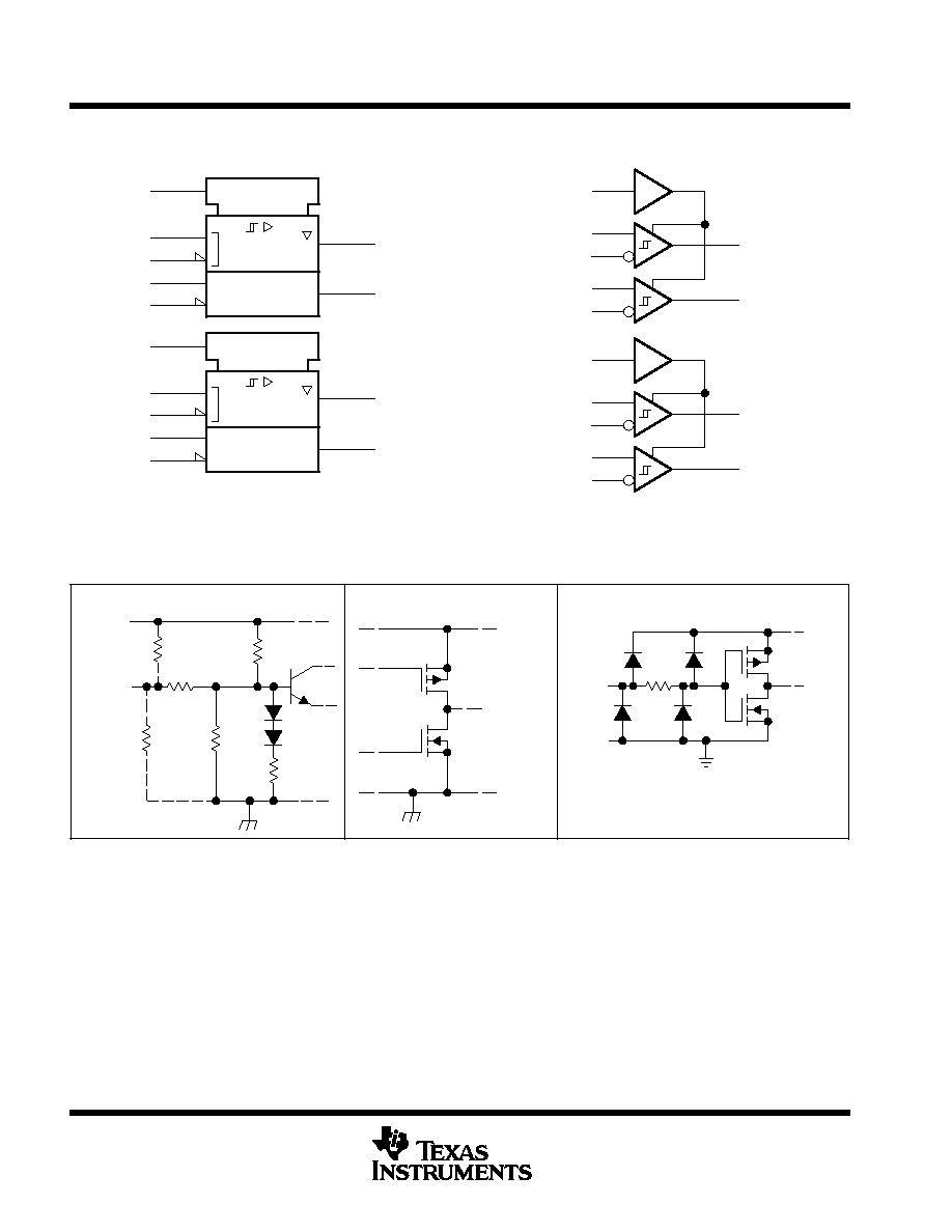
logic symbol
2B
2A
1B
1A
1, 2EN
2Y
1Y
5
3
7
6
1
2
4
EN
4B
4A
3B
3A
3, 4EN
4Y
3Y
13
11
15
14
9
10
12
EN
Pin numbers shown are for the J or W package.
This symbol is in accordance with ANSI/IEEE Std 91-1984
and IEC Publication 617-12.
logic diagram (positive logic)
2Y
1Y
5
3
7
6
1
2
4
2B
2A
1B
1A
1, 2EN
4Y
3Y
13
11
15
14
9
10
12
4B
4A
3B
3A
3, 4EN
schematics of inputs and outputs
TYPICAL OF ALL OUTPUTS
VCC
Y Output
EQUIVALENT OF A AND B INPUTS
12 k
3 k
18 k
1 k
VCC
Input
100 k
A Only
100 k
B Only
Input
VCC
TYPICAL OF EN INPUT
SN55LBC175
QUADRUPLE LOW-POWER DIFFERENTIAL LINE RECEIVER
SGLS083A ≠ MARCH 1995 ≠ REVISED JUNE 2000
3
POST OFFICE BOX 655303
∑
DALLAS, TEXAS 75265
absolute maximum ratings over operating free-air temperature range (unless otherwise noted)
Supply voltage range, V
CC
(see Note 1)
≠ 0.3 V to 7 V
. . . . . . . . . . . . . . . . . . . . . . . . . . . . . . . . . . . . . . . . . . . . . .
Input voltage, A or B inputs, V
I
±
25 V
. . . . . . . . . . . . . . . . . . . . . . . . . . . . . . . . . . . . . . . . . . . . . . . . . . . . . . . . . . . . . .
Differential input voltage, V
ID
(see Note 2)
±
25 V
. . . . . . . . . . . . . . . . . . . . . . . . . . . . . . . . . . . . . . . . . . . . . . . . . . .
Data and control voltage range
≠ 0.3 V to 7 V
. . . . . . . . . . . . . . . . . . . . . . . . . . . . . . . . . . . . . . . . . . . . . . . . . . . . . .
Continuous total dissipation
See Dissipation Rating Table
. . . . . . . . . . . . . . . . . . . . . . . . . . . . . . . . . . . . . . . . . . .
Operating free-air temperature range, T
A
≠ 55
∞
C to 125
∞
C
. . . . . . . . . . . . . . . . . . . . . . . . . . . . . . . . . . . . . . . . . . .
Storage temperature range, T
stg
≠ 65
∞
C to 150
∞
C
. . . . . . . . . . . . . . . . . . . . . . . . . . . . . . . . . . . . . . . . . . . . . . . . . . .
Lead temperature 1,6 mm (1/16 inch) from case for 10 seconds
260
∞
C
. . . . . . . . . . . . . . . . . . . . . . . . . . . . . . .
Stresses beyond those listed under "absolute maximum ratings" may cause permanent damage to the device. These are stress ratings only, and
functional operation of the device at these or any other conditions beyond those indicated under "recommended operating conditions" is not
implied. Exposure to absolute-maximum-rated conditions for extended periods may affect device reliability.
NOTES:
1. All voltage values are with respect to GND.
2. Differential input voltage is measured at the noninverting input with respect to the corresponding inverting input.
DISSIPATION RATING TABLE
PACKAGE
TA
25
∞
C
POWER RATING
DERATING FACTOR
ABOVE TA = 25
∞
C
TA = 125
∞
C
POWER RATING
FK
1375 mW
11.0 mW/
∞
C
275 mW
J
1375 mW
11.0 mW/
∞
C
275 mW
W
1000 mW
8.0 mW/
∞
C
200 mW
recommended operating conditions
MIN
NOM
MAX
UNIT
Supply voltage, VCC
4.75
5
5.25
V
Common-mode input voltage, VIC
≠ 7
12
V
Differential input voltage, VID
±
6
V
High-level input voltage, VIH
EN inputs
2
V
Low-level input voltage, VIL
EN inputs
0.8
V
High-level output current, IOH
≠ 8
mA
Low-level output current, IOL
16
mA
Operating free-air temperature, TA
≠ 55
125
∞
C
SN55LBC175
QUADRUPLE LOW-POWER DIFFERENTIAL LINE RECEIVER
SGLS083A ≠ MARCH 1995 ≠ REVISED JUNE 2000
4
POST OFFICE BOX 655303
∑
DALLAS, TEXAS 75265
electrical characteristics over recommended ranges of supply voltage and operating free-air
temperature (unless otherwise noted)
PARAMETER
TEST CONDITIONS
MIN
TYP
MAX
UNIT
VIT + Positive-going input threshold voltage
IO = ≠ 8 mA
0.2
V
VIT ≠ Negative-going input threshold voltage
IO = 8 mA
≠ 0.2
V
Vhys Hysteresis voltage ( VIT + ≠ VIT ≠ )
45
mV
VIK
Enable input clamp voltage
II = ≠ 18 mA
≠ 0.9
≠ 1.5
V
VOH
High-level output voltage
VID = 200 mV,
IOH = ≠ 8 mA
3.5
4.5
V
VOL
Low level output voltage
VID = ≠ 200 mV,
IOL = 8 mA
0.3
0.5
V
VOL
Low-level output voltage
VID = ≠ 200 mV,
IOL = 8 mA, TA = 125
∞
C
0.7
V
IOZ
High-impedance-state output current
VO = 0 V to VCC
±
20
µ
A
VIH = 12 V,
VCC = 5 V, Other inputs at 0 V
0.7
1
II
Bus input current
A or B
VIH = 12 V,
VCC = 0 V, Other inputs at 0 V
0.8
1
mA
II
Bus input current
inputs
VIH = ≠ 7 V,
VCC = 5 V, Other inputs at 0 V
≠ 0.5
≠ 0.8
mA
VIH = ≠ 7 V,
VCC = 0 V, Other inputs at 0 V
≠ 0.4
≠ 0.8
IIH
High-level enable input current
VIH = 5 V
±
20
µ
A
IIL
Low-level enable input current
VIL = 0 V
≠ 20
µ
A
IOS
Short-circuit output
current
VO = 0
≠ 80
≠ 120
mA
ICC
Supply current
Outputs enabled,
IO = 0,
VID = 5 V
11
20
mA
ICC
Supply current
Outputs disabled
0.9
1.4
mA
All typical values are at VCC = 5 V and TA = 25
∞
C.
switching characteristics, V
CC
= 5 V, C
L
= 15 pF
PARAMETER
TEST CONDITIONS
TA
MIN
TYP
MAX
UNIT
tPHL
Propagation delay time high to low level output
VID = ≠ 1.5 V to 1.5 V,
25
∞
C
11
22
30
ns
tPHL
Propagation delay time, high- to low-level output
ID
,
See Figure 1
≠ 55
∞
C to 125
∞
C
35
ns
tPLH
Propagation delay time low to high level output
VID = ≠ 1.5 V to 1.5 V,
25
∞
C
11
22
30
ns
tPLH
Propagation delay time, low- to high-level output
ID
,
See Figure 1
≠ 55
∞
C to 125
∞
C
35
ns
tPZH
Output enable time to high level
See Figure 2
25
∞
C
17
40
ns
tPZH
Output enable time to high level
See Figure 2
≠ 55
∞
C to 125
∞
C
45
ns
tPZL
Output enable time to low level
See Figure 3
25
∞
C
18
30
ns
tPZL
Output enable time to low level
See Figure 3
≠ 55
∞
C to 125
∞
C
35
ns
tPHZ
Output disable time from high level
See Figure 2
25
∞
C
30
40
ns
tPHZ
Output disable time from high level
See Figure 2
≠ 55
∞
C to 125
∞
C
55
ns
tPLZ
Output disable time from low level
See Figure 3
25
∞
C
23
30
ns
tPLZ
Output disable time from low level
See Figure 3
≠ 55
∞
C to 125
∞
C
45
ns
t k( )
Pulse skew (|tPHL tPLH|)
See Figure 1
25
∞
C
4
6
ns
tsk(p)
Pulse skew (|tPHL ≠ tPLH|)
See Figure 1
≠ 55
∞
C to 125
∞
C
7
ns
tt
Transition time
See Figure 1
25
∞
C
3
10
ns
tt
Transition time
See Figure 1
≠ 55
∞
C to 125
∞
C
16
ns
SN55LBC175
QUADRUPLE LOW-POWER DIFFERENTIAL LINE RECEIVER
SGLS083A ≠ MARCH 1995 ≠ REVISED JUNE 2000
5
POST OFFICE BOX 655303
∑
DALLAS, TEXAS 75265
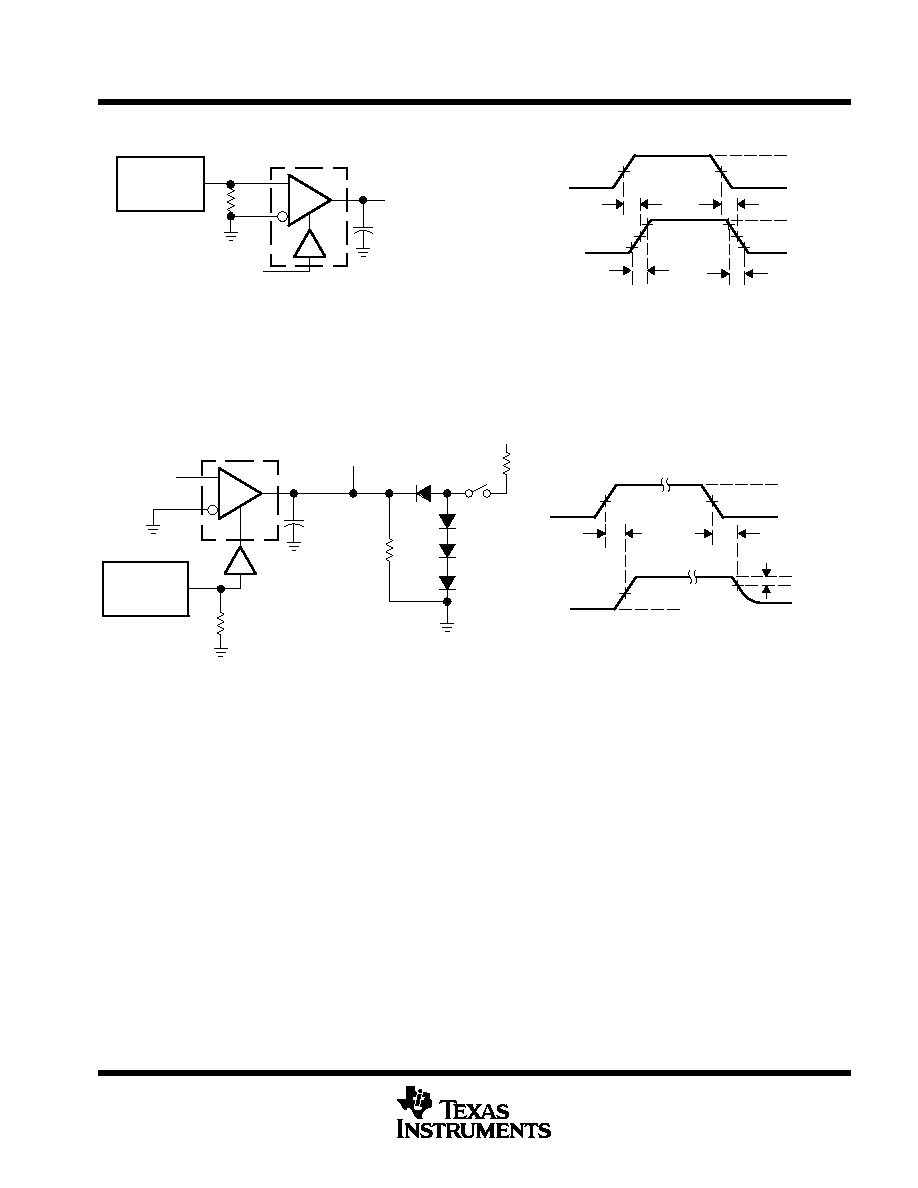
PARAMETER MEASUREMENT INFORMATION
VOL
VOH
≠ 1.5 V
1.5 V
Output
Input
1.3 V
1.3 V
tPHL
tPLH
0 V
0 V
(see Note A)
Generator
Output
(see Note B)
CL = 15 pF
50
TEST CIRCUIT
VOLTAGE WAVEFORMS
tt
tt
90%
10%
2 V
NOTES: A. The input pulse is supplied by a generator having the following characteristics: PRR = 1 MHz, duty cycle
50%, tr
6 ns, tf
6 ns, ZO = 50
.
B. CL includes probe and jig capacitance.
Figure 1. t
PLH
and t
PHL
Test Circuit and Voltage Waveforms
0 V
S1 Open
S1 Close
1.3 V
1.3 V
tPHZ
tPZH
0.5 V
See Note C
VCC
2 k
S1
5 k
1.5 V
CL = 15 pF
(see Note B)
Output
Generator
(see Note A)
1.3 V
Input
Output
3 V
0 V
VOH
1.4 V
50
TEST CIRCUIT
VOLTAGE WAVEFORMS
NOTES: A. The input pulse is supplied by a generator having the following characteristics: PRR = 1 MHz, duty cycle
50%, tr
6 ns,
tf
6 ns, ZO = 50
.
B. CL includes probe and jig capacitance.
C. All diodes are 1N916 or equivalent.
Figure 2. t
PHZ
and t
PZH
Test Circuit and Voltage Waveforms