SN55LBC173
QUADRUPLE LOW-POWER DIFFERENTIAL RECEIVER
SGLS081A ≠ MARCH 1995 ≠ REVISED JUNE 2000
1
POST OFFICE BOX 655303
∑
DALLAS, TEXAS 75265
D
Meets EIA Standards RS-422-A, RS-423-A,
RS-485, and CCITT V.11
D
Designed to Operate With Pulse Durations
as Short as 20 ns
D
Designed for Multipoint Bus Transmission
on Long Bus Lines in Noisy Environments
D
Input Sensitivity . . .
±
200 mV
D
Low-Power Consumption . . . 20 mA Max
D
Open-Circuit Fail-Safe Design
D
Pin Compatible With SN75173 and
AM26LS32
description
The SN55LBC173 is a monolithic quadruple
differential line receiver with 3-state outputs
designed to meet the requirements of the EIA
standards RS-422-A, RS-423-A, RS-485, and
CCITT V.11. This device is optimized for balanced
multipoint bus transmission at data rates up to and
exceeding 10 million bits per second. The four
receivers share two ORed enable inputs, one
active when high, the other active when low. Each
receiver features high input impedance, input
hysteresis for increased noise immunity, and input
sensitivity of
±
200 mV over a common-mode input
voltage range of 12 V to ≠7 V. Fail-safe design
ensures that if the inputs are open circuited, the
output is always high. The SN55LBC173 is
designed using the Texas Instruments proprietary
LinBiCMOS
TM
technology that provides low power
consumption, high switching speeds, and
robustness.
This device offers optimum performance when used with the SN55LBC172M quadruple line driver. The
SN55LBC173 is available in the 16-pin CDIP (J), the 16-pin CPAK (W), or the 20-pin LCCC (FK) packages.
The SN55LBC173 is characterized over the military temperature range of ≠ 55
∞
C to 125
∞
C.
Copyright
©
2000, Texas Instruments Incorporated
PRODUCTION DATA information is current as of publication date.
Products conform to specifications per the terms of Texas Instruments
standard warranty. Production processing does not necessarily include
testing of all parameters.
Please be aware that an important notice concerning availability, standard warranty, and use in critical applications of
Texas Instruments semiconductor products and disclaimers thereto appears at the end of this data sheet.
1
2
3
4
5
6
7
8
16
15
14
13
12
11
10
9
1B
1A
1Y
G
2Y
2A
2B
GND
V
CC
4B
4A
4Y
G
3Y
3A
3B
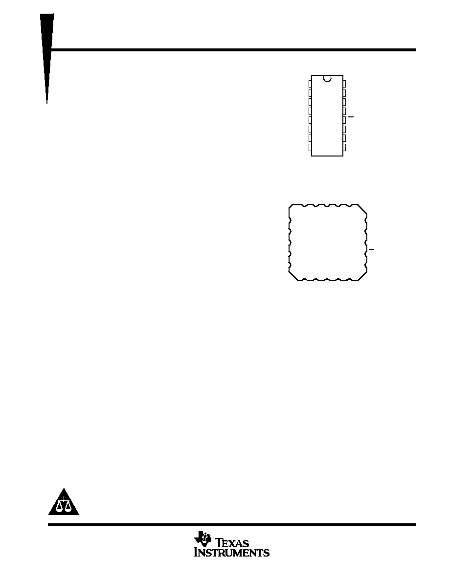
J OR W PACKAGE
(TOP VIEW)
NC ≠ No internal connection
FK PACKAGE
(TOP VIEW)
19
20
1
3
2
17
18
16
15
14
13
12
11
9
10
5
4
6
7
8
4A
4Y
NC
G
3Y
1Y
G
NC
2Y
2A
1A
1B
NC
4B
GND
NC
3B
3A
2B
V
CC
LinBiCMOS is a trademark of Texas Instruments.
SN55LBC173
QUADRUPLE LOW-POWER DIFFERENTIAL RECEIVER
SGLS081A ≠ MARCH 1995 ≠ REVISED JUNE 2000
2
POST OFFICE BOX 655303
∑
DALLAS, TEXAS 75265
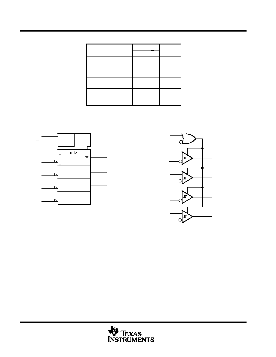
FUNCTION TABLE
(each receiver)
DIFFERENTIAL INPUTS
ENABLES
OUTPUT
A ≠ B
G
G
Y
VID
0.2 V
H
X
X
L
H
H
≠ 0.2 V < VID < 0.2 V
H
X
X
L
?
?
VID
≠ 0.2 V
H
X
X
L
L
L
X
L
H
Z
Open circuit
H
X
X
L
H
H
H = high level, L = low level, X = irrelevant,
Z = high impedance (off), ? = indeterminate
logic symbol
4B
4A
3B
3A
2B
2A
1B
1A
G
G
4Y
3Y
2Y
1Y
13
11
5
3
15
14
9
10
7
6
1
2
12
4
1
This symbol is in accordance with ANSI/IEEE Std 91-1984
and IEC Publication 617-12.
Pin numbers shown are for the J or W package.
logic diagram (positive logic)
4Y
3Y
2Y
1Y
13
11
5
3
15
14
9
10
7
6
1
2
12
4
4B
4A
3B
3A
2B
2A
1B
1A
G
G
SN55LBC173
QUADRUPLE LOW-POWER DIFFERENTIAL RECEIVER
SGLS081A ≠ MARCH 1995 ≠ REVISED JUNE 2000
3
POST OFFICE BOX 655303
∑
DALLAS, TEXAS 75265
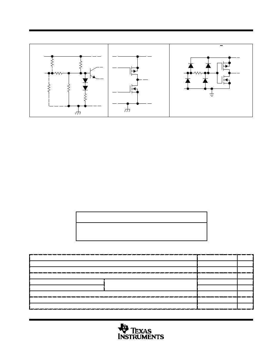
schematics of inputs and outputs
TYPICAL OF ALL OUTPUTS
VCC
Y Output
EQUIVALENT OF A AND B INPUTS
12 k
3 k
18 k
1 k
VCC
Input
100 k
A Only
100 k
B Only
Input
VCC
Receiver
TYPICAL OF G AND G INPUTS
absolute maximum ratings over operating free-air temperature range (unless otherwise noted)
Supply voltage range, V
CC
(see Note 1)
≠ 0.3 V to 7 V
. . . . . . . . . . . . . . . . . . . . . . . . . . . . . . . . . . . . . . . . . . . . . .
Input voltage, V
I
(A or B inputs)
±
25 V
. . . . . . . . . . . . . . . . . . . . . . . . . . . . . . . . . . . . . . . . . . . . . . . . . . . . . . . . . . . . .
Differential input voltage, V
ID
(see Note 2)
±
25 V
. . . . . . . . . . . . . . . . . . . . . . . . . . . . . . . . . . . . . . . . . . . . . . . . . . .
Data and control voltage range
≠ 0.3 V to 7 V
. . . . . . . . . . . . . . . . . . . . . . . . . . . . . . . . . . . . . . . . . . . . . . . . . . . . . .
Continuous total dissipation
See Dissipation Rating Table
. . . . . . . . . . . . . . . . . . . . . . . . . . . . . . . . . . . . . . . . . . .
Operating free-air temperature range, T
A
≠ 55
∞
C to 125
∞
C
. . . . . . . . . . . . . . . . . . . . . . . . . . . . . . . . . . . . . . . . . . .
Storage temperature range, T
stg
≠ 65
∞
C to 150
∞
C
. . . . . . . . . . . . . . . . . . . . . . . . . . . . . . . . . . . . . . . . . . . . . . . . . . .
Lead temperature 1,6 mm (1/16 inch) from case for 10 seconds
260
∞
C
. . . . . . . . . . . . . . . . . . . . . . . . . . . . . . .
Stresses beyond those listed under "absolute maximum ratings" may cause permanent damage to the device. These are stress ratings only, and
functional operation of the device at these or any other conditions beyond those indicated under "recommended operating conditions" is not
implied. Exposure to absolute-maximum-rated conditions for extended periods may affect device reliability.
NOTES:
1. All voltage values are with respect to GND.
2. Differential input voltage is measured at the noninverting input with respect to the corresponding inverting input.
DISSIPATION RATING TABLE
PACKAGE
TA
25
∞
C
POWER RATING
DERATING FACTOR
ABOVE TA = 25
∞
C
TA = 125
∞
C
POWER RATING
FK
1375 mW
11.0 mW/
∞
C
275 mW
J
1375 mW
11.0 mW/
∞
C
275 mW
W
1000 mW
8.0 mW/
∞
C
200 mW
recommended operating conditions
MIN
NOM
MAX
UNIT
Supply voltage, VCC
4.75
5
5.25
V
Common-mode input voltage, VIC
≠ 7
12
V
Differential input voltage, VID
±
6
V
High-level input voltage, VIH
G inputs
2
V
Low-level input voltage, VIL
G inputs
0.8
V
High-level output current, IOH
≠ 8
mA
Low-level output current, IOL
16
mA
Operating free-air temperature, TA
≠ 55
125
∞
C

SN55LBC173
QUADRUPLE LOW-POWER DIFFERENTIAL RECEIVER
SGLS081A ≠ MARCH 1995 ≠ REVISED JUNE 2000
4
POST OFFICE BOX 655303
∑
DALLAS, TEXAS 75265
electrical characteristics over recommended ranges of supply voltage and operating free-air
temperature (unless otherwise noted)
PARAMETER
TEST CONDITIONS
MIN
TYP
MAX
UNIT
VIT + Positive-going input threshold voltage
IO = ≠ 8 mA
0.2
V
VIT ≠ Negative-going input threshold voltage
IO = 8 mA
≠ 0.2
V
Vhys Hysteresis voltage ( VIT + ≠ VIT ≠ )
45
mV
VIK
Enable input clamp voltage
II = ≠ 18 mA
≠ 0.9
≠ 1.5
V
VOH
High-level output voltage
VID = 200 mV,
IOH = ≠ 8 mA
3.5
4.5
V
VOL
Low level output voltage
VID = ≠ 200 mV,
IOL = 8 mA
0.3
0.5
V
VOL
Low-level output voltage
VID = ≠ 200 mV,
IOL = 8 mA, TA = 125
∞
C
0.7
V
IOZ
High-impedance-state output current
VO = 0 V to VCC
±
20
µ
A
VIH = 12 V,
VCC = 5 V,
Other inputs at 0 V
0.7
1
II
Bus input current
A or B inputs
VIH = 12 V,
VCC = 0 V,
Other inputs at 0 V
0.8
1
mA
II
Bus input current
A or B inputs
VIH = ≠ 7 V,
VCC = 5 V,
Other inputs at 0 V
≠ 0.5
≠ 0.8
mA
VIH = ≠ 7 V,
VCC = 0 V,
Other inputs at 0 V
≠ 0.4
≠ 0.8
IIH
High-level input
current
VIH = 5 V
±
20
µ
A
IIL
Low-level input current
VIL = 0 V
≠ 20
µ
A
IOS
Short-circuit output current
VO = 0
≠ 80
≠ 120
mA
ICC
Supply current
Outputs enabled,
IO = 0,
VID = 5 V
11
20
mA
ICC
Supply current
Outputs disabled
0.9
1.4
mA
All typical values are at VCC = 5 V and TA = 25
∞
C.
switching characteristics, V
CC
= 5 V, C
L
= 15 pF
PARAMETER
TEST CONDITIONS
TA
MIN
TYP
MAX
UNIT
tPHL
Propagation delay time high to low level output
VID = ≠ 1.5 V to 1.5 V,
25
∞
C
11
22
30
ns
tPHL
Propagation delay time, high-to-low-level output
ID
,
See Figure 1
≠ 55
∞
C to 125
∞
C
11
35
ns
tPLH
Propagation delay time low to high level output
VID = ≠ 1.5 V to 1.5 V,
25
∞
C
11
22
35
ns
tPLH
Propagation delay time, low-to-high-level output
ID
,
See Figure 1
≠ 55
∞
C to 125
∞
C
11
35
ns
tPZH
Output enable time to high level
See Figure 2
25
∞
C
17
40
ns
tPZH
Output enable time to high level
See Figure 2
≠ 55
∞
C to 125
∞
C
45
ns
tPZL
Output enable time to low level
See Figure 3
25
∞
C
18
30
ns
tPZL
Output enable time to low level
See Figure 3
≠ 55
∞
C to 125
∞
C
35
ns
tPHZ
Output disable time from high level
See Figure 2
25
∞
C
30
40
ns
tPHZ
Output disable time from high level
See Figure 2
≠ 55
∞
C to 125
∞
C
55
ns
tPLZ
Output disable time from low level
See Figure 3
25
∞
C
25
40
ns
tPLZ
Output disable time from low level
See Figure 3
≠ 55
∞
C to 125
∞
C
45
ns
tsk(p)
Pulse skew (|tPHL ≠ tPLH|)
See Figure 1
25
∞
C
0.5
6
ns
tsk(p)
Pulse skew (|tPHL ≠ tPLH|)
See Figure 1
≠ 55
∞
C to 125
∞
C
7
ns
tt
Transition time
See Figure 1
25
∞
C
5
10
ns
tt
Transition time
See Figure 1
≠ 55
∞
C to 125
∞
C
16
ns

SN55LBC173
QUADRUPLE LOW-POWER DIFFERENTIAL RECEIVER
SGLS081A ≠ MARCH 1995 ≠ REVISED JUNE 2000
5
POST OFFICE BOX 655303
∑
DALLAS, TEXAS 75265
PARAMETER MEASUREMENT INFORMATION
VOL
VOH
≠ 1.5 V
1.5 V
Output
Input
1.3 V
1.3 V
tPHL
tPLH
0 V
0 V
2 V
(see Note A)
Generator
Output
(see Note B)
CL = 15 pF
50
TEST CIRCUIT
VOLTAGE WAVEFORMS
tt
tt
90%
10%
NOTES: A. The input pulse is supplied by a generator having the following characteristics: PRR = 1 MHz, duty cycle
50%, tr
6 ns,
tf
6 ns, ZO = 50
.
B. CL includes probe and jig capacitance.
Figure 1. t
pd
and t
t
Test Circuit and Voltage Waveforms
(see Note D)
0 V
S1 Open
S1 Closed
1.3 V
1.3 V
tPHZ
tPZH
0.5 V
See Note C
VCC
2 k
S1
5 k
1.5 V
CL = 15 pF
(see Note B)
Output
2 V
1.3 V
Input
Output
3 V
0 V
VOH
1.4 V
50
TEST CIRCUIT
VOLTAGE WAVEFORMS
Generator
(see Note A)
NOTES: A. The input pulse is supplied by a generator having the following characteristics: PRR = 1 MHz, duty cycle
50%, tr
6 ns,
tf
6 ns, ZO = 50
.
B. CL includes probe and jig capacitance.
C. All diodes are 1N916 or equivalent.
D. To test the active-low enable G, ground G and apply an inverted input waveform to G.
Figure 2. t
PHZ
and t
PZH
Test Circuit and Voltage Waveforms

SN55LBC173
QUADRUPLE LOW-POWER DIFFERENTIAL RECEIVER
SGLS081A ≠ MARCH 1995 ≠ REVISED JUNE 2000
6
POST OFFICE BOX 655303
∑
DALLAS, TEXAS 75265
PARAMETER MEASUREMENT INFORMATION
S2
0 V
3 V
S2 Closed
tPLZ
S2 Open
tPZL
VOL
Output
Input
1.3 V
2 V
(see Note A)
Generator
Output
(see Note B)
CL = 15 pF
≠ 1.5 V
See Note C
0.5 V
1.3 V
1.3 V
(see Note D)
50
5 k
2 k
VCC
1.4 V
TEST CIRCUIT
VOLTAGE WAVEFORMS
NOTES: A. The input pulse is supplied by a generator having the following characteristics: PRR = 1 MHz, duty cycle
50%, tr
6 ns,
tf
6 ns, ZO = 50
.
B. CL includes probe and jig capacitance.
C. All diodes are 1N916 or equivalent.
D. To test the active-low enable G, ground G and apply an inverted input waveform to G.
Figure 3. t
PZL
and t
PLZ
Test Circuit and Voltage Waveforms
TYPICAL CHARACTERISTICS
1.5
1
0.5
0
0
10
20
30
40
50
≠ Output V
oltage ≠ V
2
2.5
OUTPUT VOLTAGE
vs
DIFFERENTIAL INPUT VOLTAGE
3
60
70
80
90 100
3.5
4
4.5
V
O
VID ≠ Differential Input Voltage ≠ mV
VCC = 5 V
TA = 25
∞
C
V
IC
= 0 V
V
IC
= 12 V
V
IC
= 0 V
V
IC
= 12 V
V
IC
= ≠ 7 V
V
IC
= ≠ 7 V
Figure 4
HIGH-LEVEL OUTPUT VOLTAGE
vs
HIGH-LEVEL OUTPUT CURRENT
Figure 5
1.5
1
0.5
0
0
≠ 4
≠ 8 ≠ 12 ≠ 16 ≠ 20
≠ High-Level Output V
oltage ≠ V
2
2.5
3
≠ 24 ≠ 28 ≠ 32 ≠ 36 ≠ 40
3.5
4
4.5
V
OH
IOH ≠ High-Level Output Current ≠ mA
5
5.5
VCC = 4.75 V
VCC = 5.25 V
VCC = 5 V
VID = 0.2 V
TA = 25
∞
C
SN55LBC173
QUADRUPLE LOW-POWER DIFFERENTIAL RECEIVER
SGLS081A ≠ MARCH 1995 ≠ REVISED JUNE 2000
7
POST OFFICE BOX 655303
∑
DALLAS, TEXAS 75265
TYPICAL CHARACTERISTICS
180
120
60
0
0
3
6
9
12
15
≠ Low-Level Output V
oltage ≠ mV
240
300
LOW-LEVEL OUTPUT VOLTAGE
vs
LOW-LEVEL OUTPUT CURRENT
360
18
21
24
27
30
420
480
540
V
OL
IOL ≠ Low-Level Output Current ≠ mA
600
660
TA = 25
∞
C
VCC = 5 V
VID = 200 mV
Figure 6
AVERAGE SUPPLY CURRENT
vs
FREQUENCY
Figure 7
6
4
2
0
10 K
100 K
2 M
≠
A
verage Supply Current ≠ mA
8
10
12
10 M
100 M
14
I CC
f ≠ Frequency ≠ Hz
TA = 25
∞
C
VCC = 5 V
ŒŒŒŒŒŒŒŒŒŒŒŒŒ
ŒŒŒŒŒŒŒŒŒŒŒŒŒ
ŒŒŒŒŒŒŒŒŒŒŒŒŒ
ŒŒŒŒŒŒŒŒŒŒŒŒŒ
ŒŒŒŒŒŒŒŒŒŒŒŒŒ
ŒŒŒŒŒŒŒŒŒŒŒŒŒ
ŒŒŒŒŒŒŒŒŒŒŒŒŒ
ŒŒŒŒŒŒŒŒŒŒŒŒŒ
ŒŒŒŒŒŒŒŒŒŒŒŒŒ
ŒŒŒŒŒŒŒŒŒŒŒŒŒ
ŒŒŒŒŒŒŒŒŒŒŒŒŒ
ŒŒŒŒŒŒŒŒŒŒŒŒŒ
ŒŒŒŒŒŒŒŒŒŒŒŒŒ
ŒŒŒŒŒŒŒŒŒŒŒŒŒ
ŒŒŒŒŒŒŒŒŒŒŒŒŒ
≠ 0.4
≠ 0.6
≠ 0.8
≠ 1
≠ 8
≠ 6
≠ 4
≠ 2
0
2
≠ 0.2
0
BUS INPUT CURRENT
vs
INPUT VOLTAGE
(COMPLEMENTARY INPUT AT 0 V)
0.2
4
6
8
10
12
0.4
0.6
0.8
VI ≠ Input Voltage ≠ V
1
TA = 25
∞
C
VCC = 5 V
The shaded region of this graph represents
more than 1 unit load per RS-485.
≠ Bus Input Current ≠ mA
I I
Figure 8
23.5
23
22.5
22
≠ 40
≠ 20
0
20
40
60
Propagation Delay T
ime
≠
ns
24
24.5
PROPAGATION DELAY TIME
vs
FREE-AIR TEMPERATURE
80
100
TA ≠ Free-Air Temperature ≠
∞
C
tPHL
tPLH
VCC = 5 V
CL = 15 pF
VIO =
±
1.5 V
Figure 9

PACKAGING INFORMATION
Orderable Device
Status
(1)
Package
Type
Package
Drawing
Pins Package
Qty
Eco Plan
(2)
Lead/Ball Finish
MSL Peak Temp
(3)
5962-9076604Q2A
ACTIVE
LCCC
FK
20
1
TBD
POST-PLATE
N / A for Pkg Type
5962-9076604QEA
ACTIVE
CDIP
J
16
1
TBD
A42 SNPB
N / A for Pkg Type
5962-9076604QFA
ACTIVE
CFP
W
16
1
TBD
A42 SNPB
N / A for Pkg Type
SNJ55LBC173FK
ACTIVE
LCCC
FK
20
1
TBD
POST-PLATE
N / A for Pkg Type
SNJ55LBC173J
ACTIVE
CDIP
J
16
1
TBD
A42 SNPB
N / A for Pkg Type
SNJ55LBC173W
ACTIVE
CFP
W
16
1
TBD
A42 SNPB
N / A for Pkg Type
(1)
The marketing status values are defined as follows:
ACTIVE: Product device recommended for new designs.
LIFEBUY: TI has announced that the device will be discontinued, and a lifetime-buy period is in effect.
NRND: Not recommended for new designs. Device is in production to support existing customers, but TI does not recommend using this part in
a new design.
PREVIEW: Device has been announced but is not in production. Samples may or may not be available.
OBSOLETE: TI has discontinued the production of the device.
(2)
Eco Plan - The planned eco-friendly classification: Pb-Free (RoHS), Pb-Free (RoHS Exempt), or Green (RoHS & no Sb/Br) - please check
http://www.ti.com/productcontent
for the latest availability information and additional product content details.
TBD: The Pb-Free/Green conversion plan has not been defined.
Pb-Free (RoHS): TI's terms "Lead-Free" or "Pb-Free" mean semiconductor products that are compatible with the current RoHS requirements
for all 6 substances, including the requirement that lead not exceed 0.1% by weight in homogeneous materials. Where designed to be soldered
at high temperatures, TI Pb-Free products are suitable for use in specified lead-free processes.
Pb-Free (RoHS Exempt): This component has a RoHS exemption for either 1) lead-based flip-chip solder bumps used between the die and
package, or 2) lead-based die adhesive used between the die and leadframe. The component is otherwise considered Pb-Free (RoHS
compatible) as defined above.
Green (RoHS & no Sb/Br): TI defines "Green" to mean Pb-Free (RoHS compatible), and free of Bromine (Br) and Antimony (Sb) based flame
retardants (Br or Sb do not exceed 0.1% by weight in homogeneous material)
(3)
MSL, Peak Temp. -- The Moisture Sensitivity Level rating according to the JEDEC industry standard classifications, and peak solder
temperature.
Important Information and Disclaimer:The information provided on this page represents TI's knowledge and belief as of the date that it is
provided. TI bases its knowledge and belief on information provided by third parties, and makes no representation or warranty as to the
accuracy of such information. Efforts are underway to better integrate information from third parties. TI has taken and continues to take
reasonable steps to provide representative and accurate information but may not have conducted destructive testing or chemical analysis on
incoming materials and chemicals. TI and TI suppliers consider certain information to be proprietary, and thus CAS numbers and other limited
information may not be available for release.
In no event shall TI's liability arising out of such information exceed the total purchase price of the TI part(s) at issue in this document sold by TI
to Customer on an annual basis.
PACKAGE OPTION ADDENDUM
www.ti.com
18-Jul-2006
Addendum-Page 1


MECHANICAL DATA
MLCC006B ≠ OCTOBER 1996
POST OFFICE BOX 655303
∑
DALLAS, TEXAS 75265
FK (S-CQCC-N**)
LEADLESS CERAMIC CHIP CARRIER
4040140 / D 10/96
28 TERMINAL SHOWN
B
0.358
(9,09)
MAX
(11,63)
0.560
(14,22)
0.560
0.458
0.858
(21,8)
1.063
(27,0)
(14,22)
A
NO. OF
MIN
MAX
0.358
0.660
0.761
0.458
0.342
(8,69)
MIN
(11,23)
(16,26)
0.640
0.739
0.442
(9,09)
(11,63)
(16,76)
0.962
1.165
(23,83)
0.938
(28,99)
1.141
(24,43)
(29,59)
(19,32)
(18,78)
**
20
28
52
44
68
84
0.020 (0,51)
TERMINALS
0.080 (2,03)
0.064 (1,63)
(7,80)
0.307
(10,31)
0.406
(12,58)
0.495
(12,58)
0.495
(21,6)
0.850
(26,6)
1.047
0.045 (1,14)
0.045 (1,14)
0.035 (0,89)
0.035 (0,89)
0.010 (0,25)
12
13
14
15
16
18
17
11
10
8
9
7
5
4
3
2
0.020 (0,51)
0.010 (0,25)
6
1
28
26
27
19
21
B SQ
A SQ
22
23
24
25
20
0.055 (1,40)
0.045 (1,14)
0.028 (0,71)
0.022 (0,54)
0.050 (1,27)
NOTES: A. All linear dimensions are in inches (millimeters).
B. This drawing is subject to change without notice.
C. This package can be hermetically sealed with a metal lid.
D. The terminals are gold plated.
E. Falls within JEDEC MS-004

IMPORTANT NOTICE
Texas Instruments Incorporated and its subsidiaries (TI) reserve the right to make corrections, modifications,
enhancements, improvements, and other changes to its products and services at any time and to discontinue
any product or service without notice. Customers should obtain the latest relevant information before placing
orders and should verify that such information is current and complete. All products are sold subject to TI's terms
and conditions of sale supplied at the time of order acknowledgment.
TI warrants performance of its hardware products to the specifications applicable at the time of sale in
accordance with TI's standard warranty. Testing and other quality control techniques are used to the extent TI
deems necessary to support this warranty. Except where mandated by government requirements, testing of all
parameters of each product is not necessarily performed.
TI assumes no liability for applications assistance or customer product design. Customers are responsible for
their products and applications using TI components. To minimize the risks associated with customer products
and applications, customers should provide adequate design and operating safeguards.
TI does not warrant or represent that any license, either express or implied, is granted under any TI patent right,
copyright, mask work right, or other TI intellectual property right relating to any combination, machine, or process
in which TI products or services are used. Information published by TI regarding third-party products or services
does not constitute a license from TI to use such products or services or a warranty or endorsement thereof.
Use of such information may require a license from a third party under the patents or other intellectual property
of the third party, or a license from TI under the patents or other intellectual property of TI.
Reproduction of information in TI data books or data sheets is permissible only if reproduction is without
alteration and is accompanied by all associated warranties, conditions, limitations, and notices. Reproduction
of this information with alteration is an unfair and deceptive business practice. TI is not responsible or liable for
such altered documentation.
Resale of TI products or services with statements different from or beyond the parameters stated by TI for that
product or service voids all express and any implied warranties for the associated TI product or service and
is an unfair and deceptive business practice. TI is not responsible or liable for any such statements.
Following are URLs where you can obtain information on other Texas Instruments products and application
solutions:
Products
Applications
Amplifiers
amplifier.ti.com
Audio
www.ti.com/audio
Data Converters
dataconverter.ti.com
Automotive
www.ti.com/automotive
DSP
dsp.ti.com
Broadband
www.ti.com/broadband
Interface
interface.ti.com
Digital Control
www.ti.com/digitalcontrol
Logic
logic.ti.com
Military
www.ti.com/military
Power Mgmt
power.ti.com
Optical Networking
www.ti.com/opticalnetwork
Microcontrollers
microcontroller.ti.com
Security
www.ti.com/security
Low Power Wireless www.ti.com/lpw
Telephony
www.ti.com/telephony
Video & Imaging
www.ti.com/video
Wireless
www.ti.com/wireless
Mailing Address:
Texas Instruments
Post Office Box 655303 Dallas, Texas 75265
Copyright
2006, Texas Instruments Incorporated