TLC32044C, TLC32044E, TLC32044I, TLC32044M, TLC32045C, TLC32045I
VOICE-BAND ANALOG INTERFACE CIRCUITS
SLAS017F ≠ MARCH 1988 ≠ REVISED MAY 1995
1
POST OFFICE BOX 655303
∑
DALLAS, TEXAS 75265
D
14-Bit Dynamic Range ADC and DAC
D
2's Complement Format
D
Variable ADC and DAC Sampling Rate Up
to 19,200 Samples per Second
D
Switched-Capacitor Antialiasing Input Filter
and Output-Reconstruction Filter
D
Serial Port for Direct Interface to
TMS(SMJ)320C17, TMS(SMJ)32020,
TMS(SMJ)320C25,
and TMS320C30 Digital Signal Processors
D
Synchronous or Asynchronous ADC and
DAC Conversion Rates With Programmable
Incremental ADC and DAC Conversion
Timing Adjustments
D
Serial Port Interface to SN74(54)299
Serial-to-Parallel Shift Register for Parallel
Interface to TMS(SMJ)32010,
TMS(SMJ)320C15, or Other Digital
Processors
D
Internal Reference for Normal Operation
and External Purposes, or Can Be
Overridden by External Reference
D
CMOS Technology
description
The TLC32044 and TLC32045 are complete
analog-to-digital and digital-to-analog input and
output systems on single monolithic CMOS chips.
The TLC32044 and TLC32045 integrate a
bandpass switched-capacitor antialiasing input
filter, a 14-bit-resolution A/D converter, four
microprocessor-compatible serial port modes, a
14-bit-resolution D/A converter, and a low-pass
switched-capacitor output-reconstruction filter.
The devices offer numerous combinations of
master clock input frequencies and conversion/
sampling rates, which can be changed via digital
processor control.
Copyright
©
1995, Texas Instruments Incorporated
PRODUCTION DATA information is current as of publication date.
Products conform to specifications per the terms of Texas Instruments
standard warranty. Production processing does not necessarily include
testing of all parameters.
Please be aware that an important notice concerning availability, standard warranty, and use in critical applications of
Texas Instruments semiconductor products and disclaimers thereto appears at the end of this data sheet.
1
2
3
4
5
6
7
8
9
10
11
12
13
14
28
27
26
25
24
23
22
21
20
19
18
17
16
15
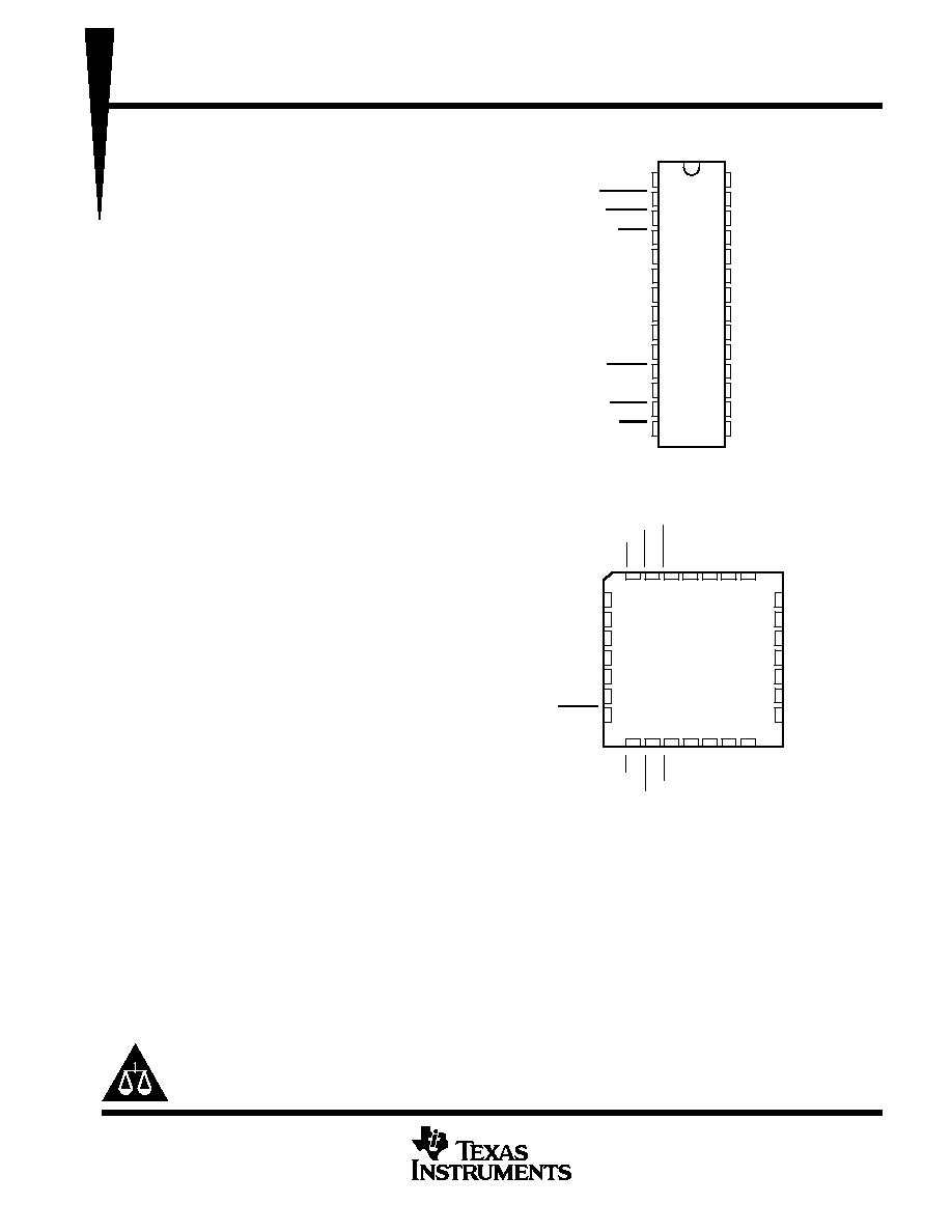
NU
RESET
EODR
FSR
DR
MSTR CLK
V
DD
REF
DGTL GND
SHIFT CLK
EODX
DX
WORD/BYTE
FSX
NU
NU
IN +
IN ≠
AUX IN +
AUX IN ≠
OUT +
OUT ≠
V
CC +
V
CC ≠
ANLG GND
ANLG GND
NU
NU
J OR N PACKAGE
(TOP VIEW)
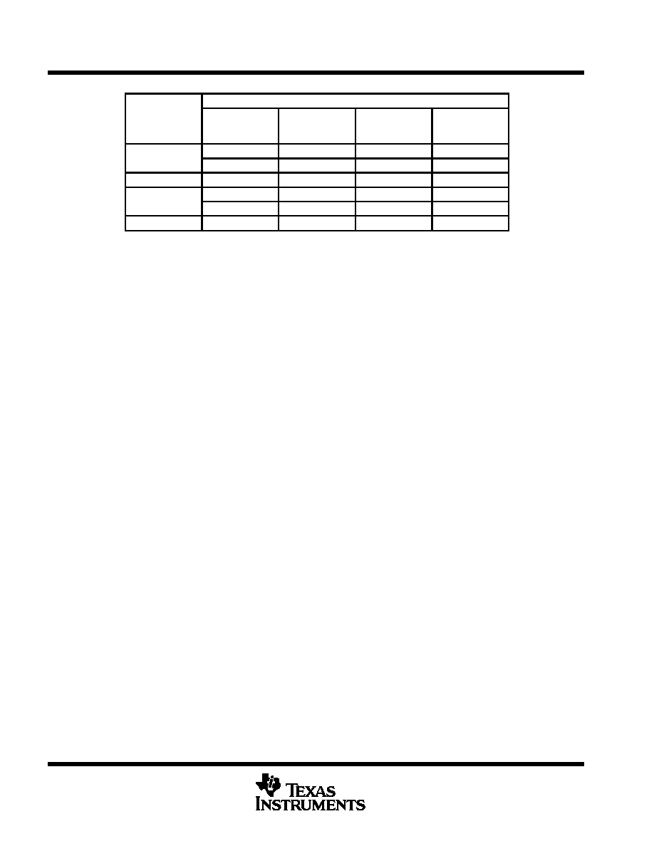
3 2
1
13 14
5
6
7
8
9
10
11
IN ≠
AUX IN +
AUX IN ≠
OUT +
OUT ≠
V
CC +
V
CC ≠
DR
MSTR CLK
V
DD
REF
DGTL GND
SHIFT CLK
EODX
4
15 16 17 18
WORD/BYTE
FSX
NU
NU
ANLG GND
ANLG GND
FSR
EODR
RESET
NU
28 27 26
25
24
23
22
21
20
19
12
DX
NU
IN +
NU
NU ≠ Nonusable; no external connection should be made to
these terminals (see Table 2).
FK OR FN PACKAGE
(TOP VIEW)
Refer to the mechanical data for the JT package.
TLC32044C, TLC32044E, TLC32044I, TLC32044M, TLC32045C, TLC32045I
VOICE-BAND ANALOG INTERFACE CIRCUITS
SLAS017F ≠ MARCH 1988 ≠ REVISED MAY 1995
2
POST OFFICE BOX 655303
∑
DALLAS, TEXAS 75265
AVAILABLE OPTIONS
PACKAGE
TA
PLASTIC CHIP
CARRIER
(FN)
PLASTIC DIP
(N)
CERAMIC DIP
(J)
CHIP CARRIER
(FK)
0
∞
C to 70
∞
C
TLC32044CFN
TLC32044CN
0
∞
C to 70
∞
C
TLC32045CFN
TLC32045CN
≠ 20
∞
C to 85
∞
C
TLC32044EFN
40
∞
C to 85
∞
C
TLC32044IN
≠ 40
∞
C to 85
∞
C
TLC32045IN
≠ 55
∞
C to 125
∞
C
TLC32044MJ
TLC32044MFK
description (continued)
Typical applications for the TLC32044 and TLC32045 include speech encryption for digital transmission,
speech recognition/ storage systems, speech synthesis, modems (7.2-, 8-, 9.6-, 14.4-, and 19.2-kHz sampling
rate), analog interface for digital signal processors (DSPs), industrial process control, biomedical
instrumentation, acoustical signal processing, spectral analysis, data acquisition, and instrumentation
recorders. Four serial modes, which allow direct interface to the TMS(SMJ)320C17, TMS(SMJ)32020,
TMS(SMJ)320C25, and TMS(SMJ)320C30 digital signal processors, are provided. Also, when the transmit and
receive sections of the analog interface circuit (AIC) are operating synchronously, it will interface to two
SN74(54)299 serial-to-parallel shift registers. These serial-to-parallel shift registers can then interface in
parallel to the TMS(SMJ)32010, TMS(SMJ)320C15, and other digital signal processors, or external FIFO
circuitry. Output data pulses are emitted to inform the processor that data transmission is complete or to allow
the DSP to differentiate between two transmitted bytes. A flexible control scheme is provided so that the
functions of the TLC32044 or TLC32045 can be selected and adjusted coincidentally with signal processing via
software control.
The antialiasing input filter comprises eighth-order and fourth-order CC-type (Chebyshev/elliptic transitional)
low-pass and high-pass filters, respectively. The input filter is implemented in switched-capacitor technology
and is preceded by a continuous time filter to eliminate any possibility of aliasing caused by sampled data
filtering. When only low-pass filtering is desired, the high-pass filter can be switched out of the signal path. A
selectable, auxiliary, differential analog input is provided for applications where more than one analog input is
required.
The A/D and D/A architectures ensure no missing codes and monotonic operation. An internal voltage reference
is provided to ease the design task and to provide complete control over the performance of the TLC32044 or
TLC32045. The internal voltage reference is brought out to a terminal and is available to the designer. Separate
analog and digital voltage supplies and grounds are provided to minimize noise and ensure a wide dynamic
range. Also, the analog circuit path contains only differential circuitry to keep noise to an absolute minimum.
The only exception is the DAC sample and hold, which utilizes pseudo-differential circuitry.
The output-reconstruction filter is an eighth-order CC-type (Chebyshev/elliptic transitional low-pass filter)
followed by a second-order (sin x) / x correction filter and is implemented in switched-capacitor technology. This
filter is followed by a continuous-time filter to eliminate images of the digitally encoded signal. The on-board
(sin x) / x correction filter can be switched out of the signal path using digital signal processor control, if desired.
The TLC32044C and TLC32045C are characterized for operation from 0
∞
C to 70
∞
C. The TLC32044E is
characterized for operation from ≠ 20
∞
C to 85
∞
C. The TLC32044I and TLC32045I are characterized for
operation from ≠ 40
∞
C to 85
∞
C. The TLC32044M is characterized for operation from ≠ 55
∞
C to 125
∞
C.

TLC32044C, TLC32044E, TLC32044I, TLC32044M, TLC32045C, TLC32045I
VOICE-BAND ANALOG INTERFACE CIRCUITS
SLAS017F ≠ MARCH 1988 ≠ REVISED MAY 1995
3
POST OFFICE BOX 655303
∑
DALLAS, TEXAS 75265
functional block diagram
M
U
X
M
U
X
IN +
IN ≠
AUX IN +
AUX IN ≠
Internal
Voltage
Reference
SHIFT CLK
MSTER CLK
EODR
DR
FSR
WORD/BYTE
DX
FSX
EODX
SERIAL
PORT
A/D
OUT +
OUT ≠
M
U
X
D/A
sin x/x
Correction
Filter
Filter
Transmit Section
VCC + VCC ≠ ANLG
GND
DTGL
GND
VDD
(Digital)
REF
RESET
Receive Section
Terminal Functions
TERMINAL
I/O
DESCRIPTION
NAME
NO.
I/O
DESCRIPTION
ANLG GND
17,18
Analog ground return for all internal analog circuits. Not internally connected to DGTL GND.
AUX IN +
24
I
Noninverting auxiliary analog input stage. AUX IN + can be switched into the bandpass filter and A/D
t
th i
ft
t l If th
i t bit i th
t l
i t
i
1 th
ili
i
t
converter path via software control. If the appropriate bit in the control register is a 1, the auxiliary inputs
will replace the IN + and IN ≠ inputs. If the bit is a 0, the IN + and IN ≠ inputs will be used (see the AIC DX
will re lace the IN + and IN ≠ in uts. If the bit is a 0, the IN + and IN ≠ in uts will be used (see the AIC DX
data word format section).
AUX IN ≠
23
I
Inverting auxiliary analog input (see the above AUX IN + description).
DGTL GND
9
Digital ground for all internal logic circuits. Not internally connected to ANLG GND.
DR
5
O
Data receive. DR is used to transmit the ADC output bits from the AIC to the TMS320 (SMJ320) serial port.
This transmission of bits from the AIC to the TMS320 (SMJ320) serial port is synchronized with the SHIFT
CLK signal.
DX
12
I
Data transmit. DX is used to receive the DAC input bits and timing and control information from the TMS320
(SMJ320). This serial transmission from the TMS320 (SMJ320) serial port to the AIC is synchronized with
the SHIFT CLK signal.
EODR
3
O
End of data receive. (See the WORD/BYTE description and Serial Port Timing diagram.) During the
word-mode timing, EODR is a low-going pulse that occurs immediately after the 16 bits of A/D information
have been transmitted from the AIC to the TMS320 (SMJ320) serial port. EODR can be used to interrupt
a microprocessor upon completion of serial communications. Also, EODR can be used to strobe and enable
external serial-to-parallel shift registers, latches, or external FIFO RAM, and to facilitate parallel data bus
communications between the AIC and the serial-to-parallel shift registers. During the byte-mode timing,
EODR goes low after the first byte has been transmitted from the AIC to the TMS320 (SMJ320) serial port
and is kept low until the second byte has been transmitted. The DSP can use this low-going signal to
differentiate between the two bytes as to which is first and which is second. EODR does not occur after
secondary communication.
TLC32044C, TLC32044E, TLC32044I, TLC32044M, TLC32045C, TLC32045I
VOICE-BAND ANALOG INTERFACE CIRCUITS
SLAS017F ≠ MARCH 1988 ≠ REVISED MAY 1995
4
POST OFFICE BOX 655303
∑
DALLAS, TEXAS 75265
Terminal Functions (continued)
TERMINAL
I/O
DESCRIPTION
NAME
NO.
I/O
DESCRIPTION
EODX
11
O
End of data transmit. (See the WORD/BYTE description and Serial Port Timing diagram.) During the
word-mode timing, EODX is a low-going pulse that occurs immediately after the 16 bits of D/A converter
and control or register information have been transmitted from the TMS320 (SMJ320) serial port to the AIC.
EODX can be used to interrupt a microprocessor upon the completion of serial communications. Also,
EODX can be used to strobe and enable external serial-to-parallel shift registers, latches, or an external
FIFO RAM, and to facilitate parallel data-bus communications between the AIC and the serial-to-parallel
shift registers. During the byte-mode timing, EODX goes low after the first byte has been transmitted from
the TMS320 (SMJ320) serial port to the AIC and is kept low until the second byte has been transmitted. The
DSP can use this low-going signal to differentiate between the two bytes as to which is first and which is
second.
FSR
4
O
Frame sync receive. In the serial transmission modes, which are described in the WORD/BYTE description,
FSR is held low during bit transmission. When FSR goes low, the TMS320 (SMJ320) serial port begins
receiving bits from the AIC via DR of the AIC. The most significant DR bit is present on DR before FSR goes
low. (See Serial Port Timing and Internal Timing Configuration diagrams.) FSR does not occur after
secondary communications.
FSX
14
O
Frame sync transmit. When FSX goes low, the TMS320 (SMJ320) serial port begins transmitting bits to the
FSX
y
g
,
(
)
g
g
AIC via DX of the AIC. In all serial transmission modes, which are described in the WORD/BYTE description,
FSX is held low during bit transmission (see Serial Port Timing and Internal Timing Configuration diagrams).
IN +
26
I
Noninverting input to analog input amplifier stage
IN ≠
25
I
Inverting input to analog input amplifier stage
MSTR CLK
6
I
Master clock. MSTR CLK is used to derive all the key logic signals of the AIC, such as the shift clock, the
switched-capacitor filter clocks, and the A/D and D/A timing signals. The Internal Timing Configuration
diagram shows how these key signals are derived. The frequencies of these key signals are synchronous
submultiples of the master clock frequency to eliminate unwanted aliasing when the sampled analog signals
are transferred between the switched-capacitor filters and the A/D and D/A converters (see the Internal
Timing Configuration diagram).
OUT +
22
O
Noninverting output of analog output power amplifier. OUT+ can drive transformer hybrids or
high-impedance loads directly in either a differential or a single-ended configuration.
OUT ≠
21
O
Inverting output of analog output power amplifier. OUT≠ is functionally identical with and complementary
to OUT +.
REF
8
I/O
Internal voltage reference. An internal reference voltage is brought out on REF. An external voltage
reference can also be applied to REF.
RESET
2
I
Reset function. RESET is provided to initialize the TA, TA', TB, RA, RA', RB, and control registers. A reset
initiates serial communications between the AIC and DSP. A reset initializes all AIC registers including the
control register. After a negative-going pulse on RESET, the AIC registers are initialized to provide an 8-khz
data conversion rate for a 5.184-MHz master clock input signal. The conversion rate adjust registers, TA'
and RA', are reset to 1. The control register bits are reset as follows (see AIC DX data word format section):
d9 = 1, d7 = 1, d6 = 1, d5 = 1, d4 = 0, d3 = 0, d2 = 1.
This initialization allows normal serial-port communication to occur between the AIC and DSP.
SHIFT CLK
10
O
Shift clock. SHIFT CLK is obtained by dividing the master clock signal frequency by four. SHIFT CLK is used
to clock the serial data transfers of the AIC, described in the WORD/BYTE description below (see the Serial
Port Timing and Internal Timing Configuration diagrams).
VDD
7
Digital supply voltage, 5 V
±
5%
VCC +
20
Positive analog supply voltage, 5 V
±
5%
VCC ≠
19
Negative analog supply voltage, ≠ 5 V
±
5%
TLC32044C, TLC32044E, TLC32044I, TLC32044M, TLC32045C, TLC32045I
VOICE-BAND ANALOG INTERFACE CIRCUITS
SLAS017F ≠ MARCH 1988 ≠ REVISED MAY 1995
5
POST OFFICE BOX 655303
∑
DALLAS, TEXAS 75265
Terminal Functions (continued)
TERMINAL
I/O
DESCRIPTION
NAME
NO.
I/O
DESCRIPTION
WORD/BYTE
13
I
Used in conjunction with a bit in the control register, WORD/BYTE is used to establish one of four serial
modes. These four serial modes are described below.
AIC transmit and receive sections are operated asynchronously.
The following description applies when the AIC is configured to have asynchronous transmit and receive
sections. If the appropriate data bit in the control register is a 0 (see the AIC DX data word format section),
the transmit and receive sections are asynchronous.
L
Serial port directly interfaces with the serial port of the DSP and communicates in two
8-bit bytes. The operation sequence is as follows (see Serial Port Timing diagrams).
1. FSX or FSR is brought low.
2. One 8-bit byte is transmitted or one 8-bit byte is received.
3. EODX or EODR is brought low.
4. FSX or FSR emits a positive frame-sync pulse that is four shift clock cycles wide.
5. One 8-bit byte is transmitted or one 8-bit byte is received.
6. EODX or EODR is brought high.
7. FSX or FSR is brought high.
H
Serial port directly interfaces with the serial ports of the TMS(SMJ)32020, TMS(SMJ)320C25, or
TMS(SMJ)320C30, and communicates in one 16-bit word. The operation sequence is as follows
(see Serial Port Timing diagrams):
1. FSX or FSR is brought low.
2. One 16-bit word is transmitted or one 16-bit word is received.
3. FSX or FSR is brought high.
4. EODX or EODR emits a low-going pulse.
AIC transmit and receive sections are operated synchronously.
If the appropriate data bit in the control register is 1, the transmit and receive sections are configured to be
synchronous. In this case, the bandpass switched-capacitor filter and the A/D conversion timing are derived
from the TX counter A, TX counter B, and TA, TA', and TB registers, rather than the RX counter A, RX counter
B, and RA, RA', and RB registers. In this case, the AIC FSX and FSR timing are identical during primary
data communication; however, FSR is not asserted during secondary data communication since there is
no new A/D conversion result. The synchronous operation sequences are as follows (see Serial Port Timing
diagrams).
L
Serial port directly interfaces with the serial port of the DSP and communicates in two 8-bit
bytes. The operation sequence is as follows (see Serial Port Timing diagrams):
1. FSX and FSR are brought low.
2. One 8-bit byte is transmitted and one 8-bit byte is received.
3. EODX and EODR are brought low.
4. FSX and FSR emit positive frame-sync pulses that are four shift clock cycles wide.
5. One 8-bit byte is transmitted and one 8-bit byte is received.
6. EODX and EODR are brought high.
7. FSX and FSR are brought high.
H
Serial port directly interfaces with the serial port of the TMS(SJM)32020, TMS(SMJ)320C25, or
TMS320C30, and communicates in one 16-bit word. The operation sequence is as follows (see
Serial Port Timing diagrams):
1. FSX and FSR are brought low.
2. One 16-bit word is transmitted and one 16-bit word is received.
3. FSX and FSR are brought high.
4. EODX or EODR emit low-going pulses.
Since the transmit and receive sections of the AIC are now synchronous, the AIC serial port with additional
NOR and AND gates interface to two SN74(54)299 serial-to-parallel shift registers. Interfacing the AIC to
the SN74(54)299 shift register allows the AIC to interface to an external FIFO RAM and facilitates parallel,
data bus communications between the AIC and the digital signal processor. The operation sequence is the
same as the above sequence (see Serial Port Timing diagrams).