TL7770-5, TL7770-12
DUAL POWER-SUPPLY SUPERVISORS
SLVS019F ≠ OCTOBER 1987 ≠ REVISED JULY 1999
1
POST OFFICE BOX 655303
∑
DALLAS, TEXAS 75265
D
Power-On Reset Generator
D
Automatic Reset Generation After Voltage
Drop
D
RESET Defined When V
CC
Exceeds 1 V
D
Wide Supply-Voltage Range . . . 3.5 V
to 18 V
D
Precision Overvoltage and Undervoltage
Sensing
D
250-mA Peak Output Current for Driving
SCR Gates
D
2-mA Active-Low SCR Gate Drive for
False-Trigger Protection
D
Temperature-Compensated Voltage
Reference
D
True and Complementary Reset Outputs
D
Externally Adjustable Output Pulse
Duration
description
The TL7770 is an integrated-circuit system supervisor designed for use as a reset controller in microcomputer
and microprocessor power-supply systems. This device contains two independent supply-voltage supervisors
that monitor the supplies for overvoltage and undervoltage conditions at the VSO and VSU terminals,
respectively. When V
CC
attains the minimum voltage of 1 V during power up, the RESET output becomes active
(low). As V
CC
approaches 3.5 V, the time-delay function activates, latching RESET and RESET active (high and
low, respectively) for a time delay (t
d
) after system voltages have achieved normal levels. Above V
CC
= 3.5 V,
taking RESIN low activates the time-delay function during normal system-voltage levels. To ensure that the
microcomputer system has reset, the outputs remain active until the voltage at VSU exceeds the threshold
value, V
IT+
, for a time delay, which is determined by an external timing capacitor such that:
t
d
[
20
10
3
capacitance
where t
d
is in seconds and capacitance is in farads.
The overvoltage-detection circuit is programmable for a wide range of designs. During an overvoltage condition,
an internal silicon-controlled rectifier (SCR) is triggered, providing 250-mA peak instantaneous current and
25-mA continuous current to the SCR gate drive terminal, which can drive an external high-current SCR gate
or an overvoltage-warning circuit.
The TL7770C series is characterized for operation from 0
∞
C to 70
∞
C. The TL7770I series is characterized for
operation from ≠40
∞
C to 85
∞
C.
Copyright
©
1999, Texas Instruments Incorporated
PRODUCTION DATA information is current as of publication date.
Products conform to specifications per the terms of Texas Instruments
standard warranty. Production processing does not necessarily include
testing of all parameters.
Please be aware that an important notice concerning availability, standard warranty, and use in critical applications of
Texas Instruments semiconductor products and disclaimers thereto appears at the end of this data sheet.
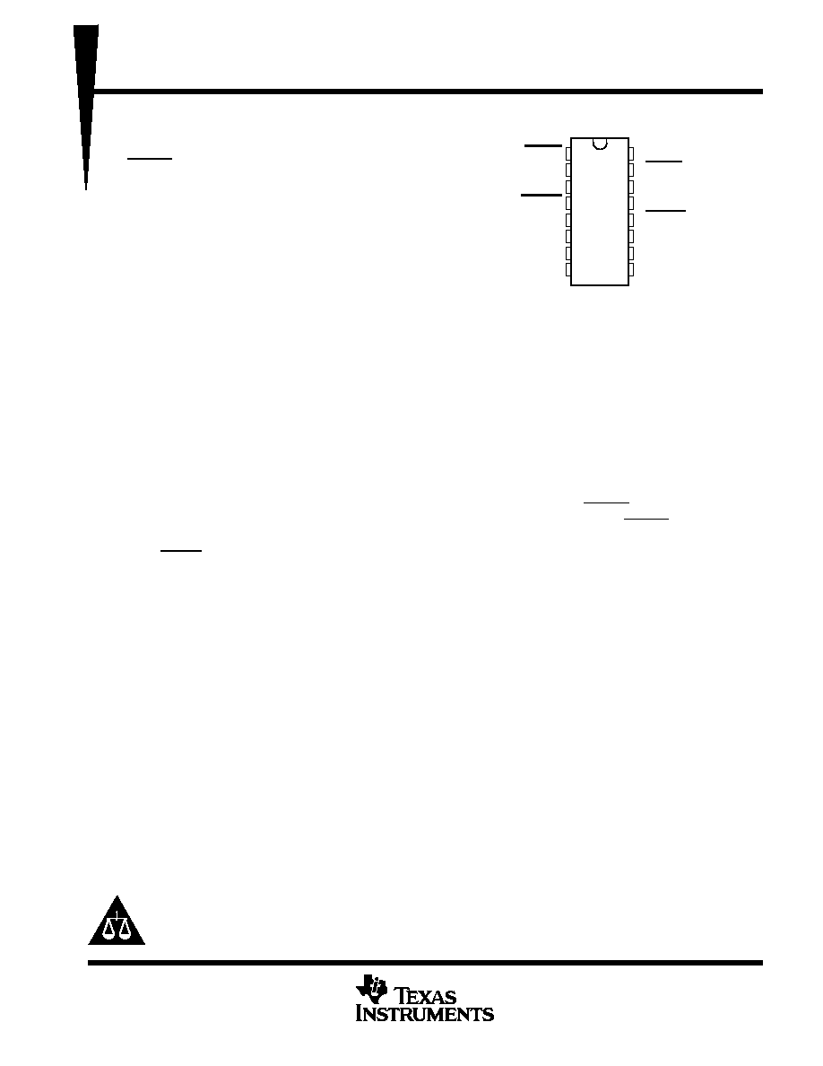
DW OR N PACKAGE
(TOP VIEW)
1
2
3
4
5
6
7
8
16
15
14
13
12
11
10
9
1RESIN
1CT
1RESET
1RESET
1VSU
1VSO
1SCR DRIVE
GND
V
CC
2RESIN
2CT
2RESET
2RESET
2VSU
2VSO
2SCR DRIVE
TL7770-5, TL7770-12
DUAL POWER-SUPPLY SUPERVISORS
SLVS019F ≠ OCTOBER 1987 ≠ REVISED JULY 1999
2
POST OFFICE BOX 655303
∑
DALLAS, TEXAS 75265
AVAILABLE OPTIONS
PACKAGED DEVICES
CHIP FORM
TA
SMALL OUTLINE
(DW)
PLASTIC DIP
(N)
CHIP FORM
(Y)
0
∞
C to 70
∞
C
TL7770-5CDW
TL7770-12CDW
TL7770-5CN
TL7770-12CN
TL7770-5Y
TL7770-12Y
≠40
∞
C to 85
∞
C
TL7770-5IDW
TL7770-5IN
--
DW package is available taped and reeled. Add the suffix R to the device type
(e.g., TL7770-5CDWR). Chip forms are tested at 25
∞
C.
functional block diagram (each channel)
65
µ
A (TYP)
R1
RESET
Vref
RESET
R2
VCC
RESIN
VSO
VSU
CT
2 mA
(TYP)
SCR DRIVE
DEVICE
1 VSU
2 VSU
R1
TL7770-5
TL7770-12
R2
R1
R2
The values listed are nominal.
24 k
70 k
10 k
10 k
Short
Short
Open
Open
TL7770-5, TL7770-12
DUAL POWER-SUPPLY SUPERVISORS
SLVS019F ≠ OCTOBER 1987 ≠ REVISED JULY 1999
3
POST OFFICE BOX 655303
∑
DALLAS, TEXAS 75265
timing requirements
RESET
VIT≠
VSU
VIT+
VCC = 1 V (TYP)
VOH
VOL
ŒŒŒŒŒŒŒ
ŒŒŒŒŒŒŒ
Undefined Operation
for VCC Less Than 1 V
VOL
VOH
VT
VSO
SCR DRIVE
td
td
td
absolute maximum ratings over operating free-air temperature range (unless otherwise noted)
Supply voltage, V
CC
(see Note 1)
20 V
. . . . . . . . . . . . . . . . . . . . . . . . . . . . . . . . . . . . . . . . . . . . . . . . . . . . . . . . . . . .
Input voltage range, V
I
: 1VSU, 2VSU, 1VSO, and 2VSO (see Note 1)
≠0.3 V to 18 V
. . . . . . . . . . . . . . . . . . . .
Low-level output current (1RESET and 2RESET), I
OL
20
mA
. . . . . . . . . . . . . . . . . . . . . . . . . . . . . . . . . . . . . . . .
High-level output current (1RESET and 2RESET), I
OH
≠20
mA
. . . . . . . . . . . . . . . . . . . . . . . . . . . . . . . . . . . . . . .
Package thermal impedance,
JA
(see Notes 2 and 3): DW package
57
∞
C/W
. . . . . . . . . . . . . . . . . . . . . . . . . . .
N package
88
∞
C/W
. . . . . . . . . . . . . . . . . . . . . . . . . . . .
Lead temperature 1,6 mm (1/16 in) from case for 10 seconds: DW or N package
260
∞
C
. . . . . . . . . . . . . . . . .
Storage temperature range, T
stg
≠65
∞
C to 150
∞
C
. . . . . . . . . . . . . . . . . . . . . . . . . . . . . . . . . . . . . . . . . . . . . . . . . . .
Stresses beyond those listed under "absolute maximum ratings" may cause permanent damage to the device. These are stress ratings only, and
functional operation of the device at these or any other conditions beyond those indicated under "recommended operating conditions" is not
implied. Exposure to absolute-maximum-rated conditions for extended periods may affect device reliability.
NOTES:
1. All voltage values are with respect to the network ground terminal.
2. Maximum power dissipation is a function of TJ(max),
JA, and TA. The maximum allowable power dissipation at any allowable
ambient temperature is PD = (TJ(max) ≠ TA)/
JA. Operating at the absolute maximum TJ of 150
∞
C can impact reliability.
3. The package thermal impedance is calculated in accordance with JESD 51, except for through-hole packages, which use a trace
length of zero.
TL7770-5, TL7770-12
DUAL POWER-SUPPLY SUPERVISORS
SLVS019F ≠ OCTOBER 1987 ≠ REVISED JULY 1999
4
POST OFFICE BOX 655303
∑
DALLAS, TEXAS 75265
recommended operating conditions
MIN
MAX
UNIT
Supply voltage, VCC
3.5
18
V
Input voltage range, VI (see Note 4)
1VSU, 2VSU, 2VSO, 1VSO
0
18
V
Output voltage, VO (1CT, 2CT)
5
V
High-level input voltage range, VIH (1RESIN, 2RESIN)
2
18
V
Low-level input voltage range, VIL (1RESIN, 2RESIN)
0
0.8
V
Output sink current, IO (1CT, 2CT)
50
µ
A
High-level output current, IOH (1RESET, 2RESET)
≠16
mA
Low-level output current, IOL (1RESET, 2RESET)
16
mA
Continuous output current, IO (1SCR DRIVE, 2SCR DRIVE)
25
mA
Timing capacitor, CT
10
µ
F
Operating free air temperature TA
TL7770C series
0
70
∞
C
Operating free-air temperature, TA
TL7770I series
≠40
85
∞
C
NOTE 4: The algebraic convention, in which the least positive (most negative) value is designated minimum, is used in this data sheet for logic
voltage levels only.
TL7770-5, TL7770-12
DUAL POWER-SUPPLY SUPERVISORS
SLVS019F ≠ OCTOBER 1987 ≠ REVISED JULY 1999
5
POST OFFICE BOX 655303
∑
DALLAS, TEXAS 75265
electrical characteristics over recommended operating conditions (unless otherwise noted)
supply supervisor section
PARAMETER
TEST
CONDITIONS
TL7770-5C
TL7770-12C
TL7770-5I
UNIT
CONDITIONS
MIN
TYP
MAX
VOH
High level output voltage
RESET
IOH = ≠15 mA
VCC≠1.5
V
VOH
High-level output voltage
SCR DRIVE
IOH = ≠20 mA
VCC≠1.5
V
VOL
Low-level output voltage
RESET
IOL = 15 mA
0.4
V
TL7770-5 (5-V sense, 1VSU)
4.46
4.64
VIT
Undervoltage input threshold
TL7770-12 (12-V sense, 1VSU)
TA = MIN to MAX
10.68
11.12
V
VIT≠
at VSU (negative-going)
TL7770-5, TL7770-12
(programmable sense, 2VSU)
TA = MIN to MAX
1.47
1.53
V
TL7770-5 (5-V sense, 1VSU)
15
Vhys
Hysteresis at VSU
TL7770-12 (12-V sense, 1VSU)
TA = MIN to MAX
36
mV
Vhys
(VIT+ ≠ VIT≠)
TL7770-5, TL7770-12
(programmable sense, 2VSU)
TA = MIN to MAX
5
mV
VT
Overvoltage threshold at VSO
TL7770-5, TL7770-12 (VSO)
TA = MIN to MAX
2.48
2.68
V
II
Input current
RESIN
VI = 5.5 V or 0.4 V
≠10
µ
A
II
Input current
VSO
VI = 2.4 V
0.5
2
µ
A
IOH
High-level output current
RESET
VO = 18 V
50
µ
A
IOL
Low-level output current
RESET
VO = 0
≠50
µ
A
IOH
Peak output current
SCR DRIVE
Duration = 1 ms
250
mA
For conditions shown as MIN or MAX, use the appropriate value specified in the recommended operating conditions.
Typical values are at VCC = 5 V, TA = 25
∞
C.
total device
PARAMETER
TEST CONDITIONS
TL7770-5C
TL7770-12C
TL7770-5I
UNIT
MIN
TYP
MAX
Vresß
Power-up reset voltage
VCC = VSU
0.8
1
V
ICC
Supply current
1VSU = 18 V, 2VSU = 2 V,
1RESIN and 2RESIN at VCC
TA = 25
∞
C
5
mA
ICC
Supply current
1RESIN and 2RESIN at VCC,
1VSO and 2VSO at 0 V
TA = MIN to MAX
6.5
mA
For conditions shown as MIN or MAX, use the appropriate value specified in the recommended operating conditions.
Typical values are at VCC = 5 V, TA = 25
∞
C.
ß This is the lowest voltage at which RESET becomes active.

TL7770-5, TL7770-12
DUAL POWER-SUPPLY SUPERVISORS
SLVS019F ≠ OCTOBER 1987 ≠ REVISED JULY 1999
6
POST OFFICE BOX 655303
∑
DALLAS, TEXAS 75265
electrical characteristics over recommended operating conditions (unless otherwise noted)
supply supervisor section
PARAMETER
TEST
CONDITIONS
TL7770-5Y
TL7770-12Y
UNIT
CONDITIONS
MIN
TYP
MAX
TL7770-5 (5-V sense, 1VSU)
4.46
4.64
VIT
Undervoltage input threshold at VSU
TL7770-12 (12-V sense, 1VSU)
TA = MIN to MAX
10.68
11.12
V
VIT≠
(negative-going)
TL7770-5, TL7770-12
(programmable sense, 2VSU)
TA = MIN to MAX
1.47
1.53
V
TL7770-5 (5-V sense, 1VSU)
15
Vhys
Hysteresis at VSU
TL7770-12 (12-V sense, 1VSU)
TA = MIN to MAX
36
mV
Vhys
(VIT+ ≠ VIT≠)
TL7770-5, TL7770-12
(programmable sense, 2VSU)
TA = MIN to MAX
5
mV
VT
Overvoltage threshold at VSO
TL7770-5, TL7770-12 (VSO)
TA = MIN to MAX
2.48
2.68
V
II
Input current
VSO
VI = 2.4 V
0.5
µ
A
Typical values are at VCC = 5 V, TA = 25
∞
C.
total device
PARAMETER
TEST CONDITIONS
TL7770-5Y
TL7770-12Y
UNIT
MIN
TYP
MAX
Vres
Power-up reset voltage
VCC = VSU,
VOL = 0.4 V, IOL = 1 mA
0.8
V
ICC
Supply current
1VSU = 18 V, 2VSU = 2 V,
1RESIN and 2RESIN at VCC,
1VSO and 2VSO at 0 V
TA = 25
∞
C
5
mA
Typical values are at VCC = 5 V, TA = 25
∞
C.
This is the lowest voltage at which RESET becomes active.
switching characteristics, V
CC
= 5 V, C
T
open, T
A
= 25
∞
C
PARAMETER
FROM
(INPUT)
TO
(OUTPUT)
TEST
CONDITIONS
MIN
TYP
MAX
UNIT
tPLH
Propagation delay time, low-to-high-level output
RESIN
RESET
270
500
ns
tPHL
Propagation delay time, high-to-low-level output
RESIN
RESET
270
500
ns
tr
Rise time
RESET
See Figures 1
75
ns
tf
Fall time
RESET
g
and 3
150
ns
tr
Rise time
RESET
75
ns
tf
Fall time
RESET
50
ns
tw(min)
Minimum effective pulse duration
RESIN
See Figure 2a
150
ns
tw(min)
Minimum effective ulse duration
VSU
See Figure 2b
100
ns

TL7770-5, TL7770-12
DUAL POWER-SUPPLY SUPERVISORS
SLVS019F ≠ OCTOBER 1987 ≠ REVISED JULY 1999
7
POST OFFICE BOX 655303
∑
DALLAS, TEXAS 75265
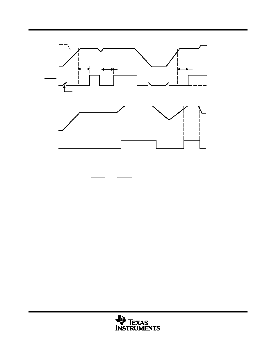
PARAMETER MEASUREMENT INFORMATION
15 pF
(see Note A)
RESET
DUT
GND
5 V
511
RESET OUTPUT CONFIGURATION
VCC
5 V
DUT
RESET
511
15 pF
(see Note A)
RESET OUTPUT CONFIGURATION
NOTE A: This includes jig and probe capacitance.
Figure 1. RESET and RESET Output Configurations
tw
5 V
2.5 V
0 V
a) RESIN
b) VSU
VIT ≠ 2 V
VIT
VIT + 2 V
tw
WAVEFORMS
Figure 2. Input Pulse Definition
10%
VIT+
VIT≠
VIT+
0 V
VIH
VIL
2 V
0.8 V
tPLH
50%
50%
10%
10%
90%
10%
td
VSU
Undefined
RESET
Voltage
Fault
tf
tr
90%
tf
td
tr
RESIN
RESET
ŒŒ
td
tPHL
10%
90%
90%
VOH
VOL
Figure 3. Voltage Waveforms
TL7770-5, TL7770-12
DUAL POWER-SUPPLY SUPERVISORS
SLVS019F ≠ OCTOBER 1987 ≠ REVISED JULY 1999
8
POST OFFICE BOX 655303
∑
DALLAS, TEXAS 75265
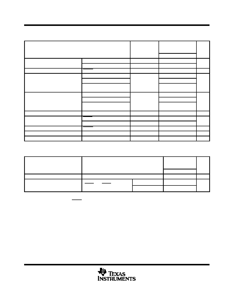
APPLICATION INFORMATION
VS
10 k
1VSU
1RESIN
GND
1RESET
1RESET
VCC
1CT
To System Reset
10 k
RT
(see Note B)
CT
System Supply
Reset Input
(from system)
To System Reset
5
1
4
3
2
8
16
NOTE B: When VCC and 1VSU are connected to the same point, it is recommended that series resistance (RT) be added between the time-delay
programming capacitor (CT) and the voltage-supervisor device terminal (1CT). The suggested RT value is given by:
R
T
u
V
I
*
V
IT
*
1
10
*
3
, where V
I
+
the lesser of 7.1 V or V
S
When this series resistor is used, the td calculation is as follows:
t
d
+
1.3
*
(6.5E
*
5)
10
*
5
R
T
6.5
10
*
5
C
T
Figure 4. System Reset Controller With Undervoltage Sensing

IMPORTANT NOTICE
Texas Instruments and its subsidiaries (TI) reserve the right to make changes to their products or to discontinue
any product or service without notice, and advise customers to obtain the latest version of relevant information
to verify, before placing orders, that information being relied on is current and complete. All products are sold
subject to the terms and conditions of sale supplied at the time of order acknowledgement, including those
pertaining to warranty, patent infringement, and limitation of liability.
TI warrants performance of its semiconductor products to the specifications applicable at the time of sale in
accordance with TI's standard warranty. Testing and other quality control techniques are utilized to the extent
TI deems necessary to support this warranty. Specific testing of all parameters of each device is not necessarily
performed, except those mandated by government requirements.
CERTAIN APPLICATIONS USING SEMICONDUCTOR PRODUCTS MAY INVOLVE POTENTIAL RISKS OF
DEATH, PERSONAL INJURY, OR SEVERE PROPERTY OR ENVIRONMENTAL DAMAGE ("CRITICAL
APPLICATIONS"). TI SEMICONDUCTOR PRODUCTS ARE NOT DESIGNED, AUTHORIZED, OR
WARRANTED TO BE SUITABLE FOR USE IN LIFE-SUPPORT DEVICES OR SYSTEMS OR OTHER
CRITICAL APPLICATIONS. INCLUSION OF TI PRODUCTS IN SUCH APPLICATIONS IS UNDERSTOOD TO
BE FULLY AT THE CUSTOMER'S RISK.
In order to minimize risks associated with the customer's applications, adequate design and operating
safeguards must be provided by the customer to minimize inherent or procedural hazards.
TI assumes no liability for applications assistance or customer product design. TI does not warrant or represent
that any license, either express or implied, is granted under any patent right, copyright, mask work right, or other
intellectual property right of TI covering or relating to any combination, machine, or process in which such
semiconductor products or services might be or are used. TI's publication of information regarding any third
party's products or services does not constitute TI's approval, warranty or endorsement thereof.
Copyright
©
1999, Texas Instruments Incorporated