
AM26C32
QUADRUPLE DIFFERENTIAL LINE RECEIVER
SLLS104I - DECEMBER 1990 - REVISED SEPTEMBER 2004
1
POST OFFICE BOX 655303
∑
DALLAS, TEXAS 75265
D
Meets or Exceeds the Requirements of
ANSI TIA/EIA-422-B, TIA/EIA-423-B, and ITU
Recommendation V.10 and V.11
D
Low Power, I
CC
= 10 mA
Typ
D
±
7-V Common-Mode Range With
±
200-mV
Sensitivity
D
Input Hysteresis . . . 60 mV Typ
D
t
pd
= 17 ns Typ
D
Operates From a Single 5-V Supply
D
3-State Outputs
D
Input Fail-Safe Circuitry
D
Improved Replacements for AM26LS32
D
Available in Q-Temp Automotive
- High Reliability Automotive Applications
- Configuration Control/Print Support
- Qualification to Automotive Standards
description/ordering information
The AM26C32 is a quadruple differential line
receiver for balanced or unbalanced digital data
transmission. The enable function is common to
all four receivers and offers a choice of active-high
or active-low input. The 3-state outputs permit
connection directly to a bus-organized system.
Fail-safe design specifies that if the inputs are
open, the outputs always are high.
The AM26C32 devices are manufactured using a BiCMOS process, which is a combination of bipolar and
CMOS transistors. This process provides the high voltage and current of bipolar with the low power of CMOS
to reduce the power consumption to about one-fifth that of the standard AM26LS32, while maintaining ac and
dc performance.
The AM26C32C is characterized for operation from 0
∞
C to 70
∞
C. The AM26C32I is characterized for operation
from -40
∞
C to 85
∞
C. The AM26C32Q is characterized for operation from -40
∞
C to 125
∞
C. The AM26C32M is
characterized for operation over the full military temperature range of -55
∞
C to 125
∞
C.
Copyright
2004, Texas Instruments Incorporated
PRODUCTION DATA information is current as of publication date.
Products conform to specifications per the terms of Texas Instruments
standard warranty. Production processing does not necessarily include
testing of all parameters.
Please be aware that an important notice concerning availability, standard warranty, and use in critical applications of
Texas Instruments semiconductor products and disclaimers thereto appears at the end of this data sheet.
1
2
3
4
5
6
7
8
16
15
14
13
12
11
10
9
1B
1A
1Y
G
2Y
2A
2B
GND
V
CC
4B
4A
4Y
G
3Y
3A
3B
AM26C32C . . . D, N, OR NS PACKAGE
AM26C32I . . . D, N, NS, OR PW PACKAGE
AM26C32Q . . . D PACKAGE
AM26C32M . . . J OR W PACKAGE
(TOP VIEW)
3
2
1 20 19
9 10 11 12 13
4
5
6
7
8
18
17
16
15
14
4A
4Y
NC
G
3Y
1Y
G
NC
2Y
2A
AM26C32M . . . FK PACKAGE
(TOP VIEW)
1A
1B
NC
3B
3A
4B
2B
GND
NC
CC
V
NC - No internal connection
On products compliant to MIL PRF 38535, all parameters are tested
unless otherwise noted. On all other products, production
processing does not necessarily include testing of all parameters.
AM26C32
QUADRUPLE DIFFERENTIAL LINE RECEIVER
SLLS104I - DECEMBER 1990 - REVISED SEPTEMBER 2004
2
POST OFFICE BOX 655303
∑
DALLAS, TEXAS 75265
description/ordering information (continued)
ORDERING INFORMATION
TA
PACKAGE
ORDERABLE
PART NUMBER
TOP-SIDE
MARKING
PDIP (N)
Tube of 25
AM26C32CN
AM26C32CN
0
∞
C to 70
∞
C
SOIC (D)
Tube of 40
AM26C32CD
AM26C32C
0
∞
C to 70
∞
C
SOIC (D)
Reel of 2500
AM26C32CDR
AM26C32C
SOP (NS)
Reel of 2000
AM26C32CNSR
26C32
PDIP (N)
Tube of 25
AM26C32IN
AM26C32IN
SOIC (D)
Tube of 40
AM26C32ID
AM26C32I
-40
∞
C to 85
∞
C
SOIC (D)
Reel of 2500
AM26C32IDR
AM26C32I
-40 C to 85 C
SOP (NS)
Reel of 2000
AM26C32INSR
26C32I
TSSOP (PW)
Tube of 90
AM26C32IPW
26C32I
-40
∞
C to 125
∞
C
SOIC (D)
Tube of 40
AM26C32QD
AM26C32QD
CDIP (J)
Tube of 25
AM26C32MJ
AM26C32MJ
- 55
∞
C to 125
∞
C
CFP (W)
Tube of 150
AM26C32MW
AM26C32MW
- 55 C to 125 C
LCCC (FK)
Tube of 55
AM26C32MFK
AM26C32MFK
Package drawings, standard packing quantities, thermal data, symbolization, and PCB design guidelines are
available at www.ti.com/sc/package.
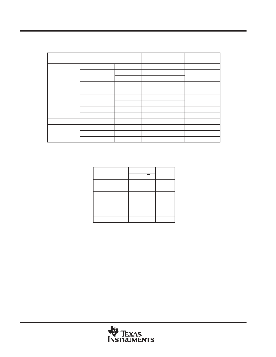
FUNCTION TABLE
(each receiver)
DIFFERENTIAL
ENABLES
OUTPUT
DIFFERENTIAL
INPUT
G
G
OUTPUT
Y
VID
VIT+
H
X
H
VID
VIT+
X
L
H
VIT- < VID < VIT+
H
X
?
VIT- < VID < VIT+
X
L
?
VID
VIT-
H
X
L
VID
VIT-
X
L
L
X
L
H
Z
H = high level, L = low level, X = irrelevant
Z = high impedance (off), ? = indeterminate
AM26C32
QUADRUPLE DIFFERENTIAL LINE RECEIVER
SLLS104I - DECEMBER 1990 - REVISED SEPTEMBER 2004
3
POST OFFICE BOX 655303
∑
DALLAS, TEXAS 75265
logic diagram (positive logic)
4Y
3Y
2Y
1Y
4B
4A
3B
3A
2B
2A
1B
1A
G
G
Pin numbers shown are for the D, J, N, NS, PW, and W packages.
4
12
2
1
6
7
10
9
14
15
3
5
11
13
schematics
Input
VCC
EQUIVALENT OF A OR B INPUT
TYPICAL OF ALL OUTPUTS
Output
VCC
VCC
1.7 k
NOM
GND
GND
1.7 k
NOM
17 k
NOM
288 k
NOM
VCC (A inputs)
or
GND (B inputs)
Input
GND
EQUIVALENT OF G OR G INPUT

AM26C32
QUADRUPLE DIFFERENTIAL LINE RECEIVER
SLLS104I - DECEMBER 1990 - REVISED SEPTEMBER 2004
4
POST OFFICE BOX 655303
∑
DALLAS, TEXAS 75265
absolute maximum ratings over operating free-air temperature range (unless otherwise noted)
Supply voltage, V
CC
(see Note 1)
7 V
. . . . . . . . . . . . . . . . . . . . . . . . . . . . . . . . . . . . . . . . . . . . . . . . . . . . . . . . . . . . .
Input voltage range, V
I
: A or B inputs
-11 V to 14 V
. . . . . . . . . . . . . . . . . . . . . . . . . . . . . . . . . . . . . . . . . . . . . . . . .
G or G inputs
-0.5 V to V
CC
+ 0.5 V
. . . . . . . . . . . . . . . . . . . . . . . . . . . . . . . . . . . . . . . . .
Differential input voltage range, V
ID
-14 V to 14 V
. . . . . . . . . . . . . . . . . . . . . . . . . . . . . . . . . . . . . . . . . . . . . . . . . .
Output voltage range, V
O
-0.5 V to V
CC
+ 0.5 V
. . . . . . . . . . . . . . . . . . . . . . . . . . . . . . . . . . . . . . . . . . . . . . . . . . . .
Output current, I
O
±
25 mA
. . . . . . . . . . . . . . . . . . . . . . . . . . . . . . . . . . . . . . . . . . . . . . . . . . . . . . . . . . . . . . . . . . . . . . .
Package thermal impedance,
JA
(see Notes 2 and 3): D package
73
∞
C/W
. . . . . . . . . . . . . . . . . . . . . . . . . . . .
N package
67
∞
C/W
. . . . . . . . . . . . . . . . . . . . . . . . . . . .
NS package
64
∞
C/W
. . . . . . . . . . . . . . . . . . . . . . . . . . .
PW package
108
∞
C/W
. . . . . . . . . . . . . . . . . . . . . . . . .
Operating virtual junction temperature, T
J
150
∞
C
. . . . . . . . . . . . . . . . . . . . . . . . . . . . . . . . . . . . . . . . . . . . . . . . . . .
Lead temperature 1,6 mm (1/16 inch) from case for 10 seconds
260
∞
C
. . . . . . . . . . . . . . . . . . . . . . . . . . . . . . .
Storage temperature range, T
stg
-65
∞
C to 150
∞
C
. . . . . . . . . . . . . . . . . . . . . . . . . . . . . . . . . . . . . . . . . . . . . . . . . . .
Stresses beyond those listed under "absolute maximum ratings" may cause permanent damage to the device. These are stress ratings only, and
functional operation of the device at these or any other conditions beyond those indicated under "recommended operating conditions" is not
implied. Exposure to absolute-maximum-rated conditions for extended periods may affect device reliability.
NOTES:
1. All voltage values, except differential output voltage, VOD, are with respect to network GND. Currents into the device are positive
and currents out of the device are negative.
2. Maximum power dissipation is a function of TJ(max),
JA, and TA. The maximum allowable power dissipation at any allowable
ambient temperature is PD = (TJ(max) - TA)/
JA. Operating at the absolute maximum TJ of 150
∞
C can affect reliability.
3. The package thermal impedance is calculated in accordance with JESD 51-7.
recommended operating conditions
MIN
NOM
MAX
UNIT
VCC
Supply voltage
4.5
5
5.5
V
VIH
High-level input voltage
2
V
VIL
Low-level input voltage
0.8
V
VIC
Common-mode input voltage
±
7
V
IOH
High-level output current
-6
mA
IOL
Low-level output current
6
mA
AM26C32C
0
70
TA
Operating free-air temperature
AM26C32I
-40
85
∞
C
TA
Operating free-air temperature
AM26C32Q
-40
125
∞
C
AM26C32M
-55
125

AM26C32
QUADRUPLE DIFFERENTIAL LINE RECEIVER
SLLS104I - DECEMBER 1990 - REVISED SEPTEMBER 2004
5
POST OFFICE BOX 655303
∑
DALLAS, TEXAS 75265
electrical characteristics over recommended ranges of V
CC
, V
IC
, and operating free-air
temperature (unless otherwise noted)
PARAMETER
TEST CONDITIONS
MIN
TYP
MAX
UNIT
VIT+
Differential input high-threshold voltage
VO = VOH(min),
VIC = -7 V to 7 V
0.2
V
VIT+
Differential input high-threshold voltage
VO = VOH(min),
IOH = -440
µ
A
VIC = 0 to 5.5 V
0.1
V
VIT-
Differential input low-threshold voltage
VO = 0.45 V,
VIC = -7 V to 7 V
-0.2
V
VIT-
Differential input low-threshold voltage
VO = 0.45 V,
IOL = 8 mA
VIC = 0 to 5.5 V
-0.1
V
Vhys
Hysteresis voltage (VIT+ - VIT-)
60
mV
VIK
Enable input clamp voltage
VCC = 4.5 V,
II = -18 mA
-1.5
V
VOH
High-level output voltage
VID = 200 mV,
IOH = -6 mA
3.8
V
VOL
Low-level output voltage
VID = -200 mV,
IOL = 6 mA
0.2
0.3
V
IOZ
Off-state (high-impedance state) output current
VO = VCC or GND
±
0.5
±
5
µ
A
II
Line input current
VI = 10 V,
Other input at 0 V
1.5
mA
II
Line input current
VI = -10 V,
Other input at 0 V
-2.5
mA
IIH
High-level enable current
VI = 2.7 V
20
µ
A
IIL
Low-level enable current
VI = 0.4 V
-100
µ
A
ri
Input resistance
One input to ground
12
17
k
ICC
Supply current
VCC = 5.5 V
10
15
mA
All typical values are at VCC = 5 V, VIC = 0, and TA = 25
∞
C.
The algebraic convention, in which the less positive (more negative) limit is designated minimum, is used in this data sheet for common-mode
input voltage.
switching characteristics over recommended ranges of operation conditions, C
L
= 50 pF (unless
otherwise noted)
PARAMETER
TEST
CONDITIONS
AM26C32C
AM26C32I
AM26C32Q
AM26C32M
UNIT
PARAMETER
CONDITIONS
MIN
TYP
MAX
MIN
TYP
MAX
UNIT
tPLH
Propagation delay time, low- to high-level output
See Figure 1
9
17
27
9
17
27
ns
tPHL
Propagation delay time, high- to low-level output
See Figure 1
9
17
27
9
17
27
ns
tTLH
Output transition time, low- to high-level output
See Figure 1
4
9
4
10
ns
tTHL
Output transition time, high- to low-level output
See Figure 1
4
9
4
9
ns
tPZH
Output enable time to high level
See Figure 2
13
22
13
22
ns
tPZL
Output enable time to low level
See Figure 2
13
22
13
22
ns
tPHZ
Output disable time from high level
See Figure 2
13
22
13
26
ns
tPLZ
Output disable time from low level
See Figure 2
13
22
13
25
ns
All typical values are at VCC = 5 V, TA = 25
∞
C.