SN54ABT245A, SN74ABT245B
OCTAL BUS TRANSCEIVERS
WITH 3 STATE OUTPUTS
SCBS081L - JANUARY 1991 - REVISED APRIL 2005
1
POST OFFICE BOX 655303
∑
DALLAS, TEXAS 75265
D
Typical V
OLP
(Output Ground Bounce)
<1 V at V
CC
= 5 V, T
A
= 25
∞
C
D
I
off
and Power-Up 3-State Support Hot
Insertion
D
High-Drive Outputs (-32-mA I
OH
, 64-mA I
OL
)
D
Latch-Up Performance Exceeds 500 mA Per
JEDEC Standard JESD 17
D
ESD Protection Exceeds JESD 22
- 2000-V Human-Body Model (A114-A)
- 200-V Machine Model (A115-A)
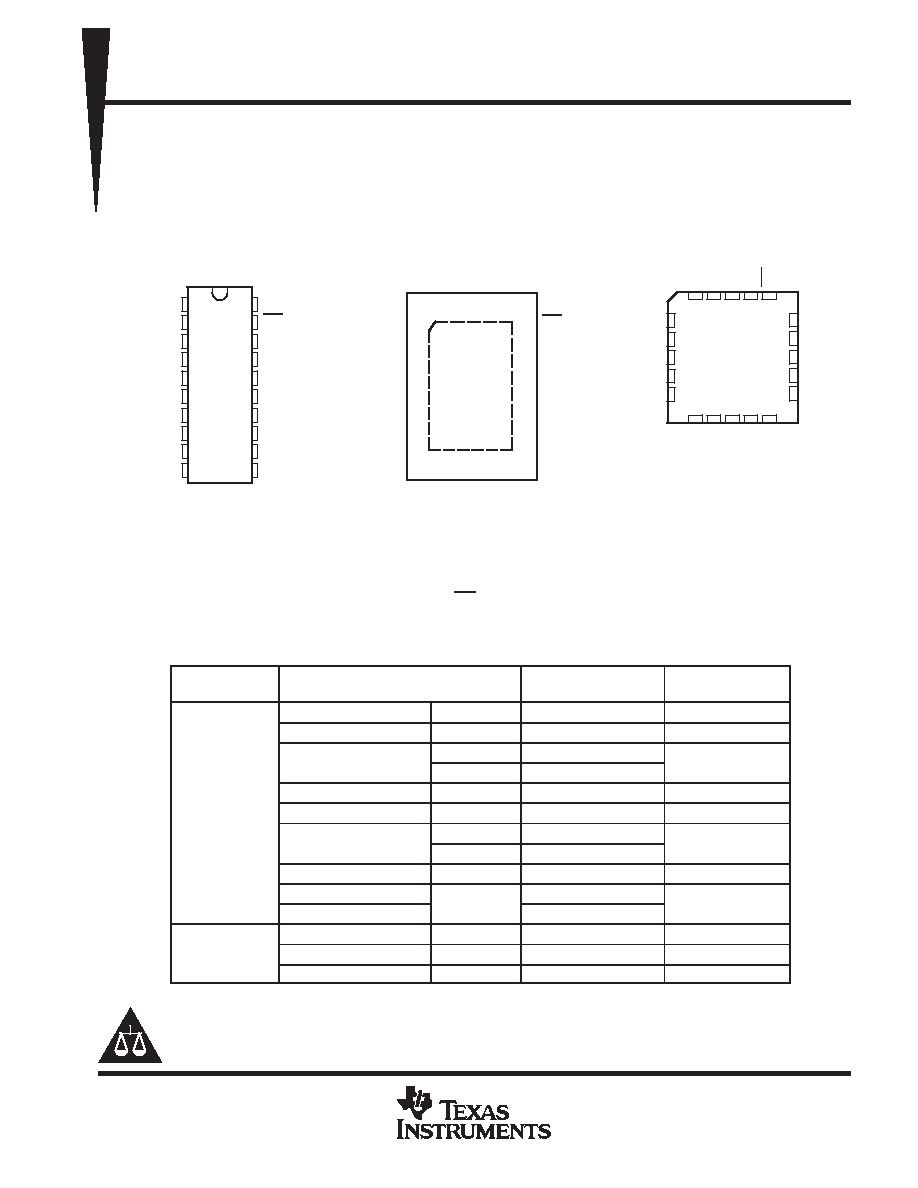
SN54ABT245A . . . J OR W PACKAGE
SN74ABT245B . . . DB, DGV, DW, N, NS,
OR PW PACKAGE
(TOP VIEW)
3
2
1 20 19
9 10 11 12 13
4
5
6
7
8
18
17
16
15
14
B1
B2
B3
B4
B5
A3
A4
A5
A6
A7
A2
A1
DIR
B7
B6
OE
A8
GND
B8
V
CC
SN54ABT245B . . . FK PACKAGE
(TOP VIEW)
1
2
3
4
5
6
7
8
9
10
20
19
18
17
16
15
14
13
12
11
DIR
A1
A2
A3
A4
A5
A6
A7
A8
GND
V
CC
OE
B1
B2
B3
B4
B5
B6
B7
B8
SN74ABT245B . . . RGY PACKAGE
(TOP VIEW)
1
20
10
11
2
3
4
5
6
7
8
9
19
18
17
16
15
14
13
12
OE
B1
B2
B3
B4
B5
B6
B7
A1
A2
A3
A4
A5
A6
A7
A8
DIR
B8
V
G
ND
CC
description/ordering information
These octal bus transceivers are designed for asynchronous communication between data buses. The devices
transmit data from the A bus to the B bus or from the B bus to the A bus, depending on the logic level at the
direction-control (DIR) input. The output-enable (OE) input can be used to disable the device so the buses are
effectively isolated.
ORDERING INFORMATION
TA
PACKAGE
ORDERABLE
PART NUMBER
TOP-SIDE
MARKING
PDIP - N
Tube
SN74ABT245BN
SN74ABT245BN
QFN - RGY
Tape and reel
SN74ABT245BRGYR
AB245B
SOIC - DW
Tube
SN74ABT245BDW
ABT245B
SOIC - DW
Tape and reel
SN74ABT245BDWR
ABT245B
SOP - NS
Tape and reel
SN74ABT245BNSR
ABT245B
-40
∞
C to 85
∞
C
SSOP - DB
Tape and reel
SN74ABT245BDBR
AB245B
-40 C to 85 C
TSSOP - PW
Tube
SN74ABT245BPW
AB245B
TSSOP - PW
Tape and reel
SN74ABT245BPWR
AB245B
TVSOP - DGV
Tape and reel
SN74ABT245BDGVR
AB245B
VFBGA - GQN
Tape and reel
SN74ABT245BGQNR
AB245B
VFBGA - ZQN (Pb-free)
Tape and reel
SN74ABT245BZQNR
AB245B
CDIP - J
Tube
SNJ54ABT245AJ
SNJ54ABT245AJ
-55
∞
C to 125
∞
C
CFP - W
Tube
SNJ54ABT245AW
SNJ54ABT245AW
-55 C to 125 C
LCCC - FK
Tube
SNJ54ABT245AFK
SNJ54ABT245AFK
Package drawings, standard packing quantities, thermal data, symbolization, and PCB design guidelines are available
at www.ti.com/sc/package.
Copyright
2005, Texas Instruments Incorporated
PRODUCTION DATA information is current as of publication date.
Products conform to specifications per the terms of Texas Instruments
standard warranty. Production processing does not necessarily include
testing of all parameters.
Please be aware that an important notice concerning availability, standard warranty, and use in critical applications of
Texas Instruments semiconductor products and disclaimers thereto appears at the end of this data sheet.
On products compliant to MIL PRF 38535, all parameters are tested
unless otherwise noted. On all other products, production
processing does not necessarily include testing of all parameters.
SN54ABT245A, SN74ABT245B
OCTAL BUS TRANSCEIVERS
WITH 3 STATE OUTPUTS
SCBS081L - JANUARY 1991 - REVISED APRIL 2005
2
POST OFFICE BOX 655303
∑
DALLAS, TEXAS 75265
description/ordering information (continued)
To ensure the high-impedance state during power up or power down, OE should be tied to V
CC
through a pullup
resistor; the minimum value of the resistor is determined by the current-sinking capability of the driver.
This device is fully specified for hot-insertion applications using I
off
and power-up 3-state. The I
off
circuitry
disables the outputs, preventing damaging current backflow through the device when it is powered down. The
power-up 3-state circuitry places the outputs in the high-impedance state during power up and power down,
which prevents driver conflict.
terminal assignments
1
2
3
4
A
A1
DIR
VCC
OE
B
A3
B2
A2
B1
C
A5
A4
B4
B3
D
A7
B6
A6
B5
E
GND
A8
B8
B7
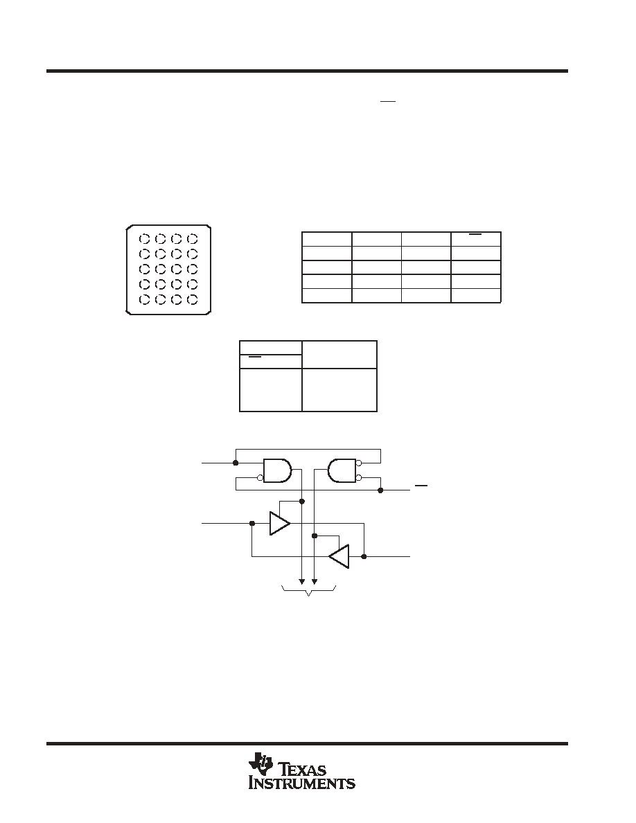
FUNCTION TABLE
INPUTS
OPERATION
OE
DIR
OPERATION
L
L
B data to A bus
L
H
A data to B bus
H
X
Isolation
logic diagram (positive logic)
DIR
OE
A1
B1
To Seven Other Channels
1
2
19
18
Pin numbers shown are for the DB, DGV, DW, FK, J, N, NS, PW, RGY, and W packages.
SN74ABT245B . . . GQN OR ZQN PACKAGE
(TOP VIEW)
1
2
3
4
A
B
C
D
E

SN54ABT245A, SN74ABT245B
OCTAL BUS TRANSCEIVERS
WITH 3 STATE OUTPUTS
SCBS081L - JANUARY 1991 - REVISED APRIL 2005
3
POST OFFICE BOX 655303
∑
DALLAS, TEXAS 75265
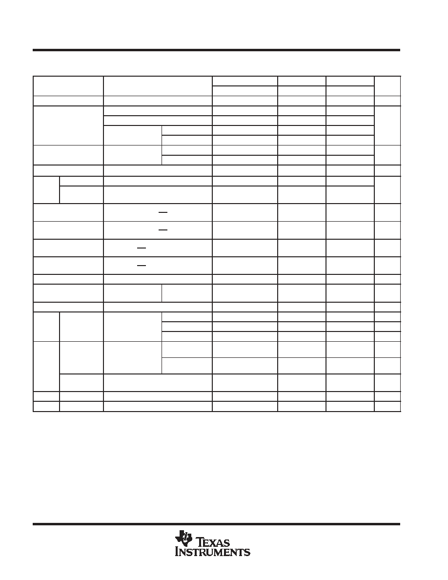
absolute maximum ratings over operating free-air temperature range (unless otherwise noted)
Supply voltage range, V
CC
-0.5 V to 7 V
. . . . . . . . . . . . . . . . . . . . . . . . . . . . . . . . . . . . . . . . . . . . . . . . . . . . . . . . . .
Input voltage range, V
I
(except I/O ports) (see Note 1)
-0.5 V to 7 V
. . . . . . . . . . . . . . . . . . . . . . . . . . . . . . . . . .
Voltage range applied to any output in the high or power-off state, V
O
-0.5 V to 5.5 V
. . . . . . . . . . . . . . . . . . .
Current into any output in the low state, I
O
: SN54ABT245A 96
mA
. . . . . . . . . . . . . . . . . . . . . . . . . . . . . . . . . . .
SN74ABT245B 128
mA
. . . . . . . . . . . . . . . . . . . . . . . . . . . . . . . . . .
Input clamp current, I
IK
(V
I
< 0)
-18 mA
. . . . . . . . . . . . . . . . . . . . . . . . . . . . . . . . . . . . . . . . . . . . . . . . . . . . . . . . . . .
Output clamp current, I
OK
(V
O
< 0)
-50 mA
. . . . . . . . . . . . . . . . . . . . . . . . . . . . . . . . . . . . . . . . . . . . . . . . . . . . . . . .
Package thermal impedance,
JA
(see Note 2): DB package
70
∞
C/W
. . . . . . . . . . . . . . . . . . . . . . . . . . . . . . . . .
(see Note 2): DGV package
92
∞
C/W
. . . . . . . . . . . . . . . . . . . . . . . . . . . . . . . .
(see Note 2): DW package
58
∞
C/W
. . . . . . . . . . . . . . . . . . . . . . . . . . . . . . . . .
(see Note 2): GQN/ZQN package
78
∞
C/W
. . . . . . . . . . . . . . . . . . . . . . . . . . .
(see Note 2): N package
69
∞
C/W
. . . . . . . . . . . . . . . . . . . . . . . . . . . . . . . . . . .
(see Note 2): NS package
60
∞
C/W
. . . . . . . . . . . . . . . . . . . . . . . . . . . . . . . . .
(see Note 2): PW package
83
∞
C/W
. . . . . . . . . . . . . . . . . . . . . . . . . . . . . . . . .
(see Note 3): RGY package
37
∞
C/W
. . . . . . . . . . . . . . . . . . . . . . . . . . . . . . . .
Storage temperature range, T
stg
-65
∞
C to 150
∞
C
. . . . . . . . . . . . . . . . . . . . . . . . . . . . . . . . . . . . . . . . . . . . . . . . . . .
Stresses beyond those listed under "absolute maximum ratings" may cause permanent damage to the device. These are stress ratings only, and
functional operation of the device at these or any other conditions beyond those indicated under "recommended operating conditions" is not
implied. Exposure to absolute-maximum-rated conditions for extended periods may affect device reliability.
NOTES:
1. The input and output negative-voltage ratings may be exceeded if the input and output clamp-current ratings are observed.
2. The package thermal impedance is calculated in accordance with JESD 51-7.
3. The package thermal impedance is calculated in accordance with JESD 51-5.
recommended operating conditions (see Note 4)
SN54ABT245A
SN74ABT245B
UNIT
MIN
MAX
MIN
MAX
UNIT
VCC
Supply voltage
4.5
5.5
4.5
5.5
V
VIH
High-level input voltage
2
2
V
VIL
Low-level input voltage
0.8
0.8
V
VI
Input voltage
0
VCC
0
VCC
V
IOH
High-level output current
-24
-32
mA
IOL
Low-level output current
48
64
mA
t/
v
Input transition rise or fall rate
5
5
ns/V
t/
VCC
Power-up ramp rate
200
µ
s/V
TA
Operating free-air temperature
-55
125
-40
85
∞
C
NOTE 4: All unused inputs of the device must be held at VCC or GND to ensure proper device operation. Refer to the TI application report,
Implications of Slow or Floating CMOS Inputs, literature number SCBA004.
SN54ABT245A, SN74ABT245B
OCTAL BUS TRANSCEIVERS
WITH 3 STATE OUTPUTS
SCBS081L - JANUARY 1991 - REVISED APRIL 2005
4
POST OFFICE BOX 655303
∑
DALLAS, TEXAS 75265
electrical characteristics over recommended operating free-air temperature range (unless
otherwise noted)
PARAMETER
TEST CONDITIONS
TA = 25
∞
C
SN54ABT245A
SN74ABT245B
UNIT
PARAMETER
TEST CONDITIONS
MIN
TYP
MAX
MIN
MAX
MIN
MAX
UNIT
VIK
VCC = 4.5 V,
II = -18 mA
-1.2
-1.2
-1.2
V
VCC = 4.5 V,
IOH = -3 mA
2.5
2.5
2.5
VOH
VCC = 5 V,
IOH = -3 mA
3
3
3
V
VOH
VCC = 4.5 V
IOH = -24 mA
2
2
V
VCC = 4.5 V
IOH = -32 mA
2*
2
VOL
VCC = 4.5 V
IOL = 48 mA
0.55
0.55
V
VOL
VCC = 4.5 V
IOL = 64 mA
0.55*
0.55
V
Vhys
100
mV
Control inputs
VCC = 0 to 5.5 V, VI = VCC or GND
±
1
±
1
±
1
II
A or B ports
VCC = 2.1 V to 5.5 V,
VI = VCC or GND
±
20
±
100
±
20
µ
A
IOZPU
VCC = 0 to 2.1 V,
VO = 0.5 V to 2.7 V, OE = X
±
50
±
50
±
50
µ
A
IOZPD
VCC = 2.1 V to 0,
VO = 0.5 V to 2.7 V, OE = X
±
50
±
50
±
50
µ
A
IOZH
VCC = 2.1 V to 5.5 V,
VO = 2.7 V, OE
2 V
10
10
10
µ
A
IOZL
VCC = 2.1 V to 5.5 V,
VO = 0.5 V, OE
2 V
-10
-10
-10
µ
A
Ioff
VCC = 0,
VI or VO
5.5 V
±
100
±
100
µ
A
ICEX
VCC = 5.5 V,
VO = 5.5 V
Outputs high
50
50
50
µ
A
IOß
VCC = 5.5 V,
VO = 2.5 V
-50
-140
-180
-50
-180
-50
-180
mA
VCC = 5.5 V,
Outputs high
5
250
250
250
µ
A
ICC
A or B ports
VCC = 5.5 V,
IO = 0,
V = V
or GND
Outputs low
22
30
30
30
mA
ICC
A or B ports
IO = 0,
VI = VCC or GND
Outputs disabled
1
250
250
250
µ
A
Data inputs
VCC = 5.5 V,
One input at 3.4 V,
Outputs enabled
1.5
1.5
1.5
mA
ICC∂
Data inputs
One input at 3.4 V,
Other inputs at
VCC or GND
Outputs disabled
50
50
50
µ
A
CC
Control inputs
VCC = 5.5 V, One input at 3.4 V,
Other inputs at VCC or GND
1.5
1.5
1.5
mA
Ci
Control inputs
VI = 2.5 V or 0.5 V
4
pF
Cio
A or B ports
VO = 2.5 V or 0.5 V
8
pF
* On products compliant to MIL-PRF-38535, this parameter does not apply.
All typical values are at VCC = 5 V.
The parameters IOZH and IOZL include the input leakage current.
ß Not more than one output should be tested at a time, and the duration of the test should not exceed one second.
∂ This is the increase in supply current for each input that is at the specified TTL voltage level, rather than VCC or GND.
SN54ABT245A, SN74ABT245B
OCTAL BUS TRANSCEIVERS
WITH 3 STATE OUTPUTS
SCBS081L - JANUARY 1991 - REVISED APRIL 2005
5
POST OFFICE BOX 655303
∑
DALLAS, TEXAS 75265
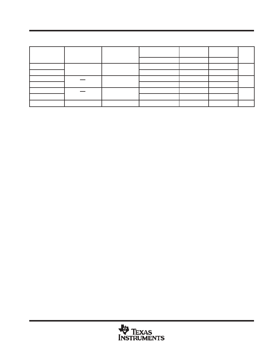
switching characteristics over recommended ranges of supply voltage and operating free-air
temperature, C
L
= 50 pF (unless otherwise noted) (see Figure 1)
PARAMETER
FROM
(INPUT)
TO
(OUTPUT)
VCC = 5 V,
TA = 25
∞
C
SN54ABT245A
SN74ABT245B
UNIT
PARAMETER
(INPUT)
(OUTPUT)
MIN
TYP
MAX
MIN
MAX
MIN
MAX
UNIT
tPLH
A or B
B or A
1
2
3.2
0.8
3.8
1
3.6
ns
tPHL
A or B
B or A
1
2.6
3.5
1
4.2
1
3.9
ns
tPZH
OE
A or B
2
3.5
4.5
1.2
6.2
2
5.6
ns
tPZL
OE
A or B
1.9
4
5.3
1.3
6.8
1.9
6.2
ns
tPHZ
OE
A or B
2.2
4.4
5.4
2.2
6.1
2.2
5.9
ns
tPLZ
OE
A or B
1.5
3
4
1.0
4.9
1.5
4.5
ns
tsk(o)
0.5
0.5
ns