CY54FCT240T, CY74FCT240T
8-BIT BUFFERS/LINE DRIVERS
WITH 3-STATE OUTPUTS
SCCS017A ≠ MAY 1994 ≠ REVISED OCTOBER 2001
1
POST OFFICE BOX 655303
∑
DALLAS, TEXAS 75265
D
Function, Pinout, and Drive Compatible
With FCT and F Logic
D
Reduced V
OH
(Typically = 3.3 V) Versions
of Equivalent FCT Functions
D
Edge-Rate Control Circuitry for
Significantly Improved Noise
Characteristics
D
I
off
Supports Partial-Power-Down Mode
Operation
D
ESD Protection Exceeds JESD 22
≠ 2000-V Human-Body Model (A114-A)
≠ 200-V Machine Model (A115-A)
≠ 1000-V Charged-Device Model (C101)
D
Matched Rise and Fall Times
D
Fully Compatible With TTL Input and
Output Logic Levels
D
CY54FCT240T
≠ 48-mA Output Sink Current
12-mA Output Source Current
D
CY74FCT240T
≠ 64-mA Output Sink Current
32-mA Output Source Current
D
3-State Outputs
description
The 'FCT240T devices are octal buffers and line
drivers designed to be employed as memory
address drivers, clock drivers, and
bus-oriented transmitters/receivers. These devices provide speed and drive capabilities equivalent to their
fastest bipolar logic counterparts, while reducing power consumption. The input and output voltage levels allow
direct interface with TTL, NMOS, and CMOS devices without external components.
These devices are fully specified for partial-power-down applications using I
off
. The I
off
circuitry disables the
outputs, preventing damaging current backflow through the device when it is powered down.
Copyright
2001, Texas Instruments Incorporated
PRODUCTION DATA information is current as of publication date.
Products conform to specifications per the terms of Texas Instruments
standard warranty. Production processing does not necessarily include
testing of all parameters.
Please be aware that an important notice concerning availability, standard warranty, and use in critical applications of
Texas Instruments semiconductor products and disclaimers thereto appears at the end of this data sheet.
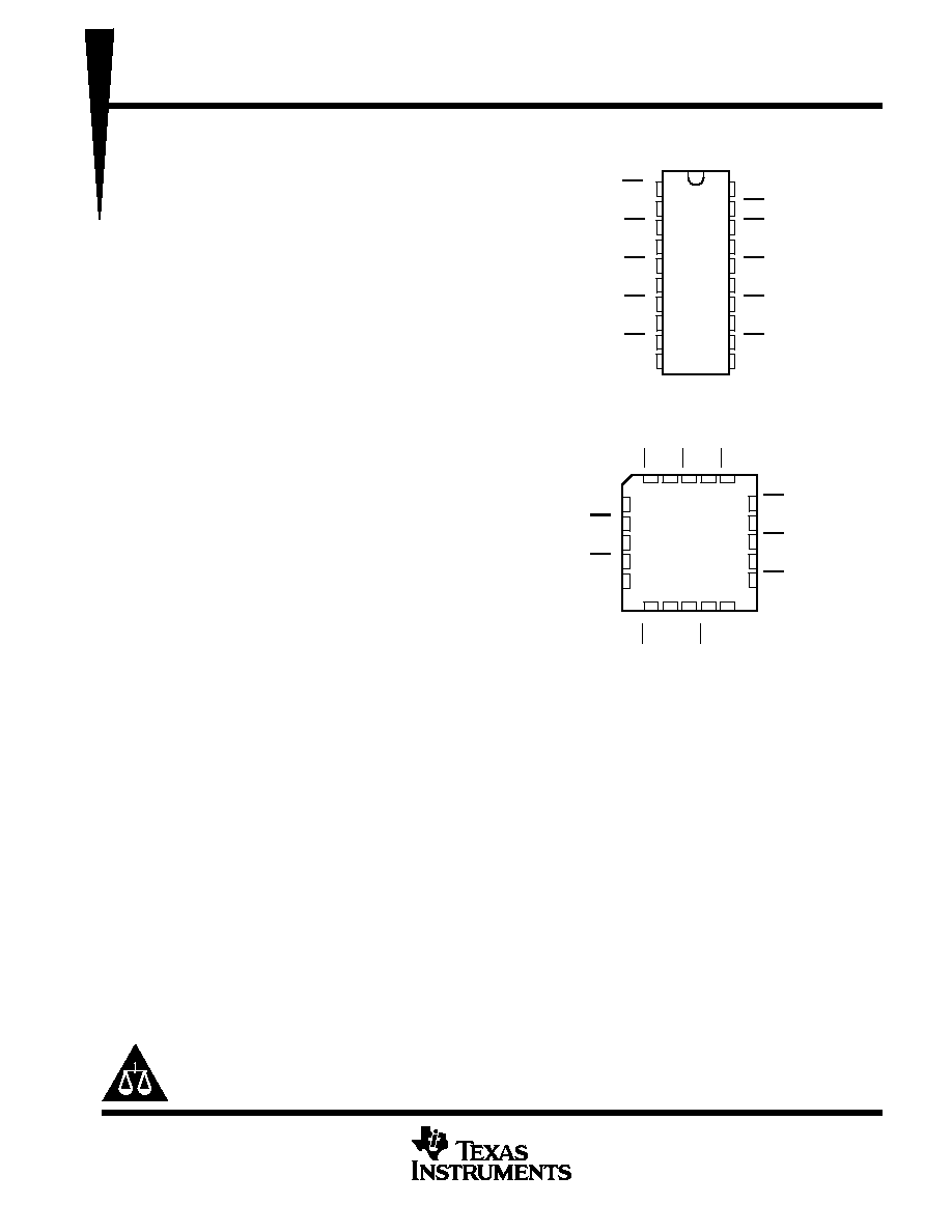
CY54FCT240T . . . L PACKAGE
(TOP VIEW)
1
2
3
4
5
6
7
8
9
10
20
19
18
17
16
15
14
13
12
11
OE
A
DA
0
OB
0
DA
1
OB
1
DA
2
OB
2
DA
3
OB
3
GND
V
CC
OE
B
OA
0
DB
0
OA
1
DB
1
OA
2
DB
2
OA
3
DB
3
CY54FCT240T . . . D PACKAGE
CY74FCT240T . . . Q OR SO PACKAGE
(TOP VIEW)
3
2 1 20 19
9 10 11 12 13
4
5
6
7
8
18
17
16
15
14
OA
0
DB
0
OA
1
DB
1
OA
2
OB
DA
OE
OA
DB
V
OE
OB
GND
DB
CC
DA
1
OB
1
DA
2
OB
2
DA
3
0
0
A
B
3
3
3
2
On products compliant to MIL-PRF-38535, all parameters are tested
unless otherwise noted. On all other products, production
processing does not necessarily include testing of all parameters.
CY54FCT240T, CY74FCT240T
8-BIT BUFFERS/LINE DRIVERS
WITH 3-STATE OUTPUTS
SCCS017A ≠ MAY 1994 ≠ REVISED OCTOBER 2001
2
POST OFFICE BOX 655303
∑
DALLAS, TEXAS 75265
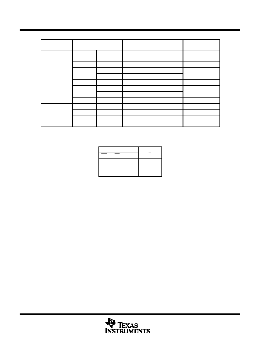
ORDERING INFORMATION
TA
PACKAGE
SPEED
(ns)
ORDERABLE
PART NUMBER
TOP-SIDE
MARKING
SOIC
SO
Tube
4.3
CY74FCT240CTSOC
FCT240C
SOIC ≠ SO
Tape and reel
4.3
CY74FCT240CTSOCT
FCT240C
QSOP ≠ Q
Tape and reel
4.3
CY74FCT240CTQCT
FCT240C
SOIC
SO
Tube
4.8
CY74FCT240ATSOC
FCT240A
≠40
∞
C to 85
∞
C
SOIC ≠ SO
Tape and reel
4.8
CY74FCT240ATSOCT
FCT240A
QSOP ≠ Q
Tape and reel
4.8
CY74FCT240ATQCT
FCT240A
SOIC
SO
Tube
8
CY74FCT240TSOC
FCT240
SOIC ≠ SO
Tape and reel
8
CY74FCT240TSOCT
FCT240
QSOP ≠ Q
Tape and reel
8
CY74FCT240TQCT
FCT240
CDIP ≠ D
Tube
4.7
CY54FCT240CTDMB
55
∞
C to 125
∞
C
CDIP ≠ D
Tube
5.1
CY54FCT240ATDMB
≠55
∞
C to 125
∞
C
LCC ≠ L
Tube
5.1
CY54FCT240ATLMB
CDIP ≠ D
Tube
9
CY54FCT240TDMB
Package drawings, standard packing quantities, thermal data, symbolization, and PCB design guidelines are available
at www.ti.com/sc/package.
FUNCTION TABLE
INPUTS
OUTPUT
OEA
OEB
D
O
L
L
L
H
L
L
H
L
H
H
X
Z
H = High logic level, L = Low logic level,
X = Don't care, Z = High-impedance state
CY54FCT240T, CY74FCT240T
8-BIT BUFFERS/LINE DRIVERS
WITH 3-STATE OUTPUTS
SCCS017A ≠ MAY 1994 ≠ REVISED OCTOBER 2001
3
POST OFFICE BOX 655303
∑
DALLAS, TEXAS 75265
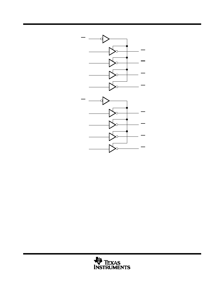
logic diagram (positive logic)
1
2
4
6
8
12
14
16
18
OEA
DA0
OA0
DA2
OA2
19
17
15
13
11
9
7
5
3
OEB
DB1
OB1
DB3
OB3
DA1
OA1
DA3
OA3
DB0
OB0
DB2
OB2
absolute maximum rating over operating free-air temperature range (unless otherwise noted)
Supply voltage range to ground potential
≠0.5 V to 7 V
. . . . . . . . . . . . . . . . . . . . . . . . . . . . . . . . . . . . . . . . . . . . . .
DC input voltage range
≠0.5 V to 7 V
. . . . . . . . . . . . . . . . . . . . . . . . . . . . . . . . . . . . . . . . . . . . . . . . . . . . . . . . . . . . . .
DC output voltage range
≠0.5 V to 7 V
. . . . . . . . . . . . . . . . . . . . . . . . . . . . . . . . . . . . . . . . . . . . . . . . . . . . . . . . . . . .
DC output current (maximum sink current/pin)
120 mA
. . . . . . . . . . . . . . . . . . . . . . . . . . . . . . . . . . . . . . . . . . . . . . .
Package thermal impedance,
JA
(see Note 1): Q package
68
∞
C/W
. . . . . . . . . . . . . . . . . . . . . . . . . . . . . . . . . .
SO package
58
∞
C/W
. . . . . . . . . . . . . . . . . . . . . . . . . . . . . . . . .
Ambient temperature range with power applied, T
A
≠65
∞
C to 135
∞
C
. . . . . . . . . . . . . . . . . . . . . . . . . . . . . . . . . . .
Storage temperature range, T
stg
≠65
∞
C to 150
∞
C
. . . . . . . . . . . . . . . . . . . . . . . . . . . . . . . . . . . . . . . . . . . . . . . . . . .
Stresses beyond those listed under "absolute maximum ratings" may cause permanent damage to the device. These are stress ratings only, and
functional operation of the device at these or any other conditions beyond those indicated under "recommended operating conditions" is not implied.
Exposure to absolute-maximum-rated conditions for extended periods may affect device reliability.
NOTE 1: The package thermal impedance is calculated in accordance with JESD 51-7.
CY54FCT240T, CY74FCT240T
8-BIT BUFFERS/LINE DRIVERS
WITH 3-STATE OUTPUTS
SCCS017A ≠ MAY 1994 ≠ REVISED OCTOBER 2001
4
POST OFFICE BOX 655303
∑
DALLAS, TEXAS 75265
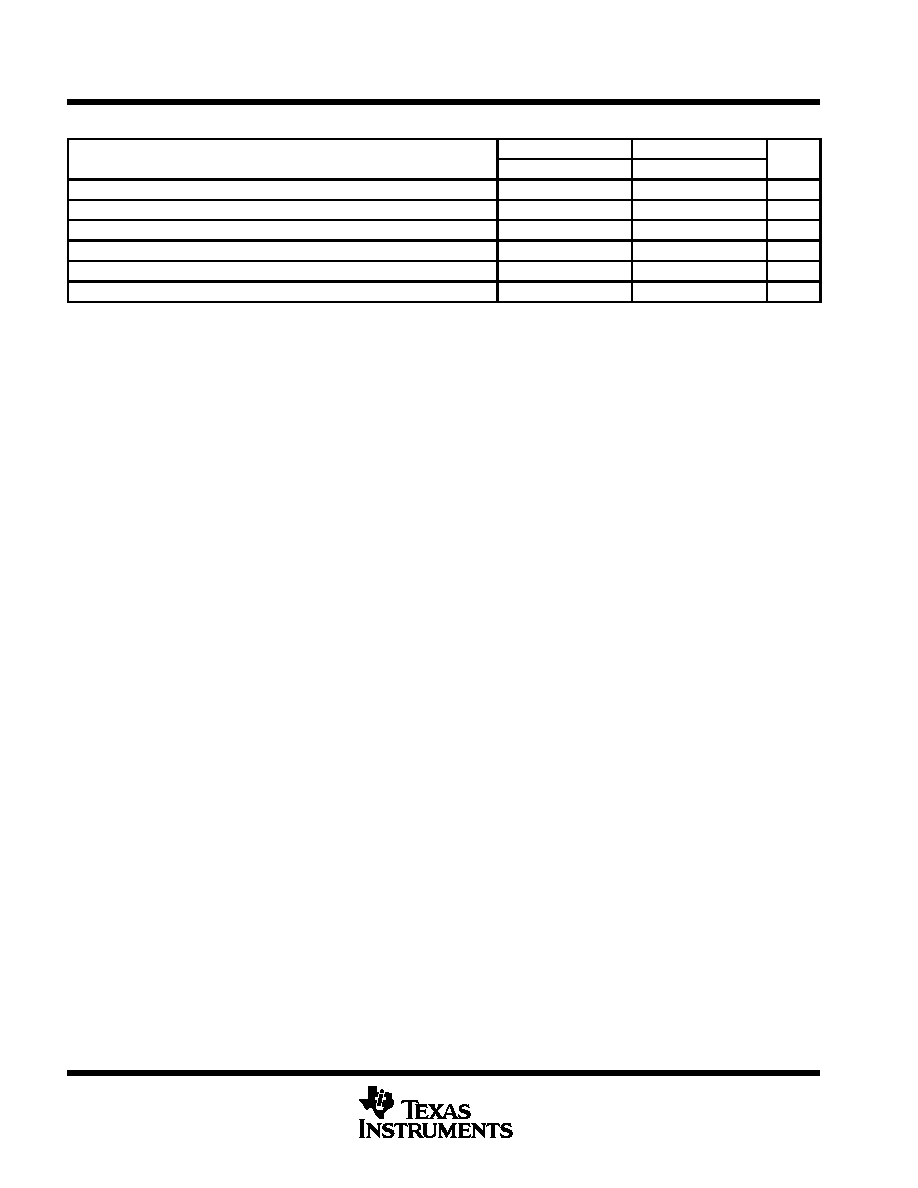
recommended operating conditions (see Note 2)
CY54FCT240T
CY74FCT240T
UNIT
MIN
NOM
MAX
MIN
NOM
MAX
UNIT
VCC
Supply voltage
4.5
5
5.5
4.75
5
5.25
V
VIH
High-level input voltage
2
2
V
VIL
Low-level input voltage
0.8
0.8
V
IOH
High-level output current
≠12
≠32
mA
IOL
Low-level output current
48
64
mA
TA
Operating free-air temperature
≠55
125
≠40
85
∞
C
NOTE 2: All unused inputs of the device must be held at VCC
or GND to ensure proper device operation.
CY54FCT240T, CY74FCT240T
8-BIT BUFFERS/LINE DRIVERS
WITH 3-STATE OUTPUTS
SCCS017A ≠ MAY 1994 ≠ REVISED OCTOBER 2001
5
POST OFFICE BOX 655303
∑
DALLAS, TEXAS 75265
electrical characteristics over recommended operating free-air temperature range (unless
otherwise noted)
PARAMETER
TEST CONDITIONS
CY54FCT240T
CY74FCT240T
UNIT
PARAMETER
TEST CONDITIONS
MIN
TYP
MAX
MIN
TYP
MAX
UNIT
VIK
VCC = 4.5 V,
IIN = ≠18 mA
≠0.7
≠1.2
V
VIK
VCC = 4.75 V,
IIN = ≠18 mA
≠0.7
≠1.2
V
VCC = 4.5 V,
IOH = ≠12 mA
2.4
3.3
VOH
VCC 4 75 V
IOH = ≠32 mA
2
V
VCC = 4.75 V
IOH = ≠15 mA
2.4
3.3
VOL
VCC = 4.5 V,
IOL = 48 mA
0.3
0.55
V
VOL
VCC = 4.75 V,
IOL = 64 mA
0.3
0.55
V
Vhys
All inputs
0.2
0.2
V
II
VCC = 5.5 V,
VIN = VCC
5
µ
A
II
VCC = 5.25 V,
VIN = VCC
5
µ
A
IIH
VCC = 5.5 V,
VIN = 2.7 V
±
1
µ
A
IIH
VCC = 5.25 V,
VIN = 2.7 V
±
1
µ
A
IIL
VCC = 5.5 V,
VIN = 0.5 V
±
1
µ
A
IIL
VCC = 5.25 V,
VIN = 0.5 V
±
1
µ
A
IOZH
VCC = 5.5 V,
VOUT = 2.7 V
10
µ
A
IOZH
VCC = 5.25 V,
VOUT = 2.7 V
10
µ
A
IOZL
VCC = 5.5 V,
VOUT = 0.5 V
≠10
µ
A
IOZL
VCC = 5.25 V,
VOUT = 0.5 V
≠10
µ
A
IOS
VCC = 5.5 V,
VOUT = 0 V
≠60
≠120
≠225
mA
IOS
VCC = 5.25 V,
VOUT = 0 V
≠60
≠120
≠225
mA
Ioff
VCC = 0 V,
VOUT = 4.5 V
±
1
±
1
µ
A
ICC
VCC = 5.5 V,
VIN
0.2 V,
VIN
VCC ≠ 0.2 V
0.1
0.2
mA
ICC
VCC = 5.25 V,
VIN
0.2 V,
VIN
VCC ≠ 0.2 V
0.1
0.2
mA
ICC
VCC = 5.5 V, VIN = 3.4 Vß, f1 = 0, Outputs open
0.5
2
mA
ICC
VCC = 5.25 V, VIN = 3.4 Vß, f1 = 0, Outputs open
0.5
2
mA
ICCD∂
VCC = 5.5 V, One input switching at 50% duty cycle,
Outputs open, OEA = OEB = GND,
VIN
0.2 V or VIN
VCC ≠ 0.2 V
0.06
0.12
mA/
ICCD∂
VCC = 5.25 V, One input switching at 50% duty cycle,
Outputs open, OEA = OEB = GND,
VIN
0.2 V or VIN
VCC ≠ 0.2 V
0.06
0.12
MHz
Typical values are at VCC = 5 V, TA = 25
∞
C.
Not more than one output should be shorted at a time. Duration of short should not exceed one second. The use of high-speed test apparatus and/or
sample-and-hold techniques are preferable to minimize internal chip heating and more accurately reflect operational values. Otherwise, prolonged
shorting of a high output can raise the chip temperature well above normal and cause invalid readings in other parametric tests. In any sequence
of parameter tests, IOS tests should be performed last.
ß Per TTL-driven input (VIN = 3.4 V); all other inputs at VCC or GND
∂ This parameter is derived for use in total power-supply calculations.