"1-of-8 Decoders"
CY54FCT138T, CY74FCT138T
1-OF-8 DECODERS
SCCS013B MAY 1994 REVISED OCTOBER 2001
1
POST OFFICE BOX 655303
·
DALLAS, TEXAS 75265
D
Function, Pinout, and Drive Compatible
With FCT and F Logic
D
Reduced V
OH
(Typically = 3.3 V) Versions of
Equivalent FCT Functions
D
Edge-Rate Control Circuitry for
Significantly Improved Noise
Characteristics
D
I
off
Supports Partial-Power-Down Mode
Operation
D
Matched Rise and Fall Times
D
Fully Compatible With TTL Input and
Output Logic Levels
D
Dual 1-of-8 Decoder With Enables
D
ESD Protection Exceeds JESD 22
2000-V Human-Body Model (A114-A)
200-V Machine Model (A115-A)
1000-V Charged-Device Model (C101)
D
CY54FCT138T
32-mA Output Sink Current
12-mA Output Source Current
D
CY74FCT138T
64-mA Output Sink Current
32-mA Output Source Current
description
The 'FCT138T devices are 1-of-8 decoders. These devices accept three binary weighted inputs (A
0
, A
1
, A
2
)
and, when enabled, provide eight mutually exclusive active-low outputs (O
0
O
7
). The 'FCT138T devices
feature three enable inputs: two active low (E
1
, E
2
) and one active high (E
3
).
All outputs are high unless E
1
and E
2
are low and E
3
is high. This multiple-enable function allows easy parallel
expansion of the device to a 1-of-32 (five lines to 32 lines) decoder with just four 'FCT138T devices and one
inverter.
These devices are fully specified for partial-power-down applications using I
off
. The I
off
circuitry disables the
outputs, preventing damaging current backflow through the device when it is powered down.
PIN DESCRIPTION
NAME
DESCRIPTION
A
Address inputs
E1, E2
Enable inputs (active low)
E3
Enable input (active high)
O
Outputs
Copyright
2001, Texas Instruments Incorporated
PRODUCTION DATA information is current as of publication date.
Products conform to specifications per the terms of Texas Instruments
standard warranty. Production processing does not necessarily include
testing of all parameters.
Please be aware that an important notice concerning availability, standard warranty, and use in critical applications of
Texas Instruments semiconductor products and disclaimers thereto appears at the end of this data sheet.
1
2
3
4
5
6
7
8
16
15
14
13
12
11
10
9
A
0
A
1
A
2
E
1
E
2
E
3
O
7
GND
V
CC
O
0
O
1
O
2
O
3
O
4
O
5
O
6
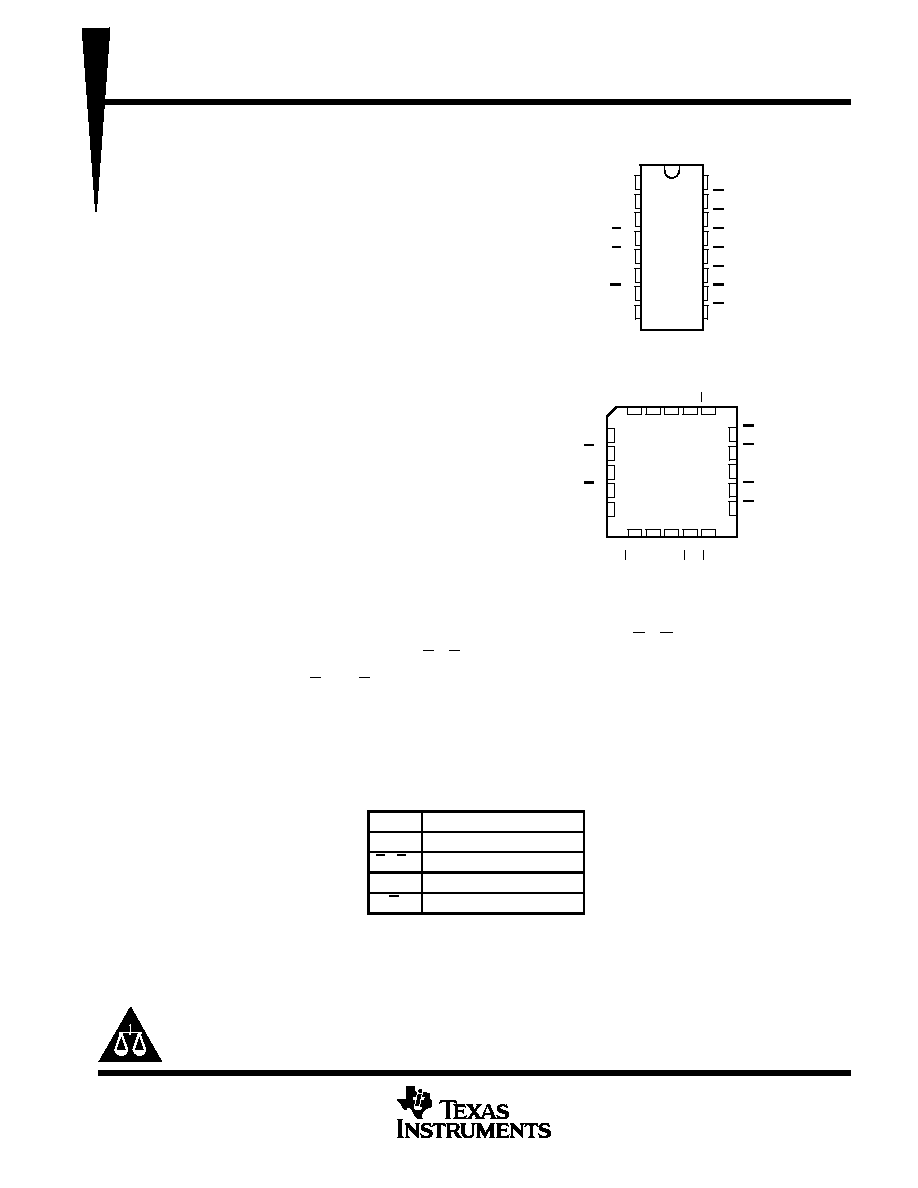
CY54FCT138T . . . D PACKAGE
CY74FCT138T . . . Q OR SO PACKAGE
(TOP VIEW)
3
2 1 20 19
9 10 11 12 13
4
5
6
7
8
18
17
16
15
14
O
1
O
2
NC
O
3
O
4
A
2
E
1
NC
E
2
E
3
A
NC
V
7
GND
NC
CY54FCT138T . . . L PACKAGE
(TOP VIEW)
CC
NC No internal connection
1
A
0
O
0
O
6
O
5
O
On products compliant to MIL-PRF-38535, all parameters are tested
unless otherwise noted. On all other products, production
processing does not necessarily include testing of all parameters.
CY54FCT138T, CY74FCT138T
1-OF-8 DECODERS
SCCS013B MAY 1994 REVISED OCTOBER 2001
2
POST OFFICE BOX 655303
·
DALLAS, TEXAS 75265
ORDERING INFORMATION
TA
PACKAGE
SPEED
(ns)
ORDERABLE
PART NUMBER
TOP-SIDE
MARKING
QSOP Q
Tape and reel
5
CY74FCT138CTQCT
FT138-3
SOIC
SO
Tube
5
CY74FCT138CTSOC
FCT138C
SOIC SO
Tape and reel
5
CY74FCT138CTSOCT
FCT138C
40
°
C to 85
°
C
QSOP Q
Tape and reel
5.8
CY74FCT138ATQCT
FT138-1
SOIC
SO
Tube
5.8
CY74FCT138ATSOC
FCT138A
SOIC SO
Tape and reel
5.8
CY74FCT138ATSOCT
FCT138A
QSOP Q
Tape and reel
9
CY74FCT138TQCT
FT138
LCC L
Tube
6
CY54FCT138CTLMB
55
°
C to 125
°
C
LCC L
Tube
12
CY54FCT138TLMB
CDIP D
Tube
12
CY54FCT138TDMB
Package drawings, standard packing quantities, thermal data, symbolization, and PCB design guidelines are
available at www.ti.com/sc/package.
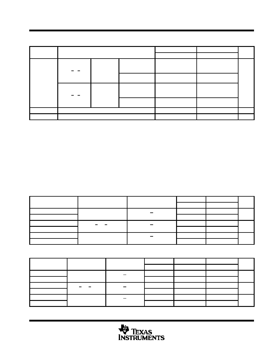
FUNCTION TABLE
INPUTS
OUTPUTS
E1
E2
E3
A0
A1
A2
O0
O1
O2
O3
O4
O5
O6
O7
H
X
X
X
X
X
H
H
H
H
H
H
H
H
X
H
X
X
X
X
H
H
H
H
H
H
H
H
X
X
L
X
X
X
H
H
H
H
H
H
H
H
L
L
H
L
L
L
L
H
H
H
H
H
H
H
L
L
H
H
L
L
H
L
H
H
H
H
H
H
L
L
H
L
H
L
H
H
L
H
H
H
H
H
L
L
H
H
H
L
H
H
H
L
H
H
H
H
L
L
H
L
L
H
H
H
H
H
L
H
H
H
L
L
H
H
L
H
H
H
H
H
H
L
H
H
L
L
H
L
H
H
H
H
H
H
H
H
L
H
L
L
H
H
H
H
H
H
H
H
H
H
H
L
H = High logic level, L = Low logic level, X = Don't care
CY54FCT138T, CY74FCT138T
1-OF-8 DECODERS
SCCS013B MAY 1994 REVISED OCTOBER 2001
3
POST OFFICE BOX 655303
·
DALLAS, TEXAS 75265
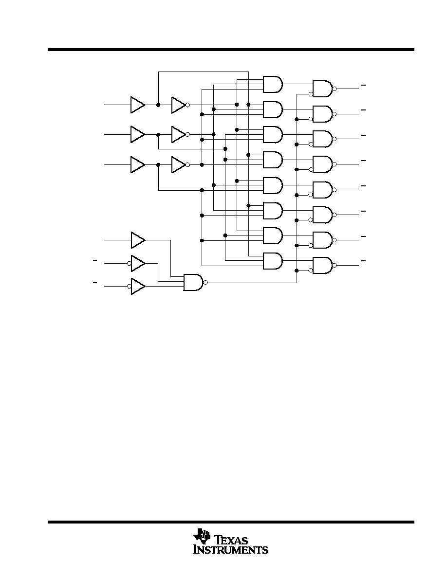
logic diagram (positive logic)
E2
E1
E3
A2
A1
A0
O0
1
2
3
6
4
5
15
14
13
12
11
10
9
7
Pin numbers shown are for the D, Q, and SO packages.
O1
O2
O3
O4
O5
O6
O7
absolute maximum ratings over operating free-air temperature range (unless otherwise noted)
Supply voltage range to ground potential
0.5 V to 7 V
. . . . . . . . . . . . . . . . . . . . . . . . . . . . . . . . . . . . . . . . . . . . . .
DC input voltage range
0.5 V to 7 V
. . . . . . . . . . . . . . . . . . . . . . . . . . . . . . . . . . . . . . . . . . . . . . . . . . . . . . . . . . . . .
DC output voltage range
0.5 V to 7 V
. . . . . . . . . . . . . . . . . . . . . . . . . . . . . . . . . . . . . . . . . . . . . . . . . . . . . . . . . . . .
DC output current (maximum sink current/pin)
120 mA
. . . . . . . . . . . . . . . . . . . . . . . . . . . . . . . . . . . . . . . . . . . . . .
Package thermal impedance,
JA
(see Note 1): Q package
90
°
C/W
. . . . . . . . . . . . . . . . . . . . . . . . . . . . . . . . . .
SO package
57
°
C/W
. . . . . . . . . . . . . . . . . . . . . . . . . . . . . . . . .
Ambient temperature range with power applied, T
A
65
°
C to 135
°
C
. . . . . . . . . . . . . . . . . . . . . . . . . . . . . . . . . . .
Storage temperature range, T
stg
65
°
C to 150
°
C
. . . . . . . . . . . . . . . . . . . . . . . . . . . . . . . . . . . . . . . . . . . . . . . . . . .
Stresses beyond those listed under "absolute maximum ratings" may cause permanent damage to the device. These are stress ratings only, and
functional operation of the device at these or any other conditions beyond those indicated under "recommended operating conditions" is not
implied. Exposure to absolute-maximum-rated conditions for extended periods may affect device reliability.
NOTE 1: The package thermal impedance is calculated in accordance with JESD 51-7.
CY54FCT138T, CY74FCT138T
1-OF-8 DECODERS
SCCS013B MAY 1994 REVISED OCTOBER 2001
4
POST OFFICE BOX 655303
·
DALLAS, TEXAS 75265
recommended operating conditions (see Note 2)
CY54FCT138T
CY74FCT138T
UNIT
MIN
NOM
MAX
MIN
NOM
MAX
UNIT
VCC
Supply voltage
4.5
5
5.5
4.75
5
5.25
V
VIH
High-level input voltage
2
2
V
VIL
Low-level input voltage
0.8
0.8
V
IOH
High-level output current
12
32
mA
IOL
Low-level output current
32
64
mA
TA
Operating free-air temperature
55
125
40
85
°
C
NOTE 2: All unused inputs of the device must be held at VCC or GND to ensure proper device operation.
electrical characteristics over recommended operating free-air temperature range (unless
otherwise noted)
PARAMETER
TEST CONDITIONS
CY54FCT138T
CY74FCT138T
UNIT
PARAMETER
TEST CONDITIONS
MIN
TYP
MAX
MIN
TYP
MAX
UNIT
VIK
VCC = 4.5 V,
IIN = 18 mA
0.7
1.2
V
VIK
VCC = 4.75 V,
IIN = 18 mA
0.7
1.2
V
VCC = 4.5 V,
IOH = 12 mA
2.4
3.3
VOH
VCC = 4 75 V
IOH = 32 mA
2
V
VCC = 4.75 V
IOH = 15 mA
2.4
3.3
VOL
VCC = 4.5 V,
IOL = 32 mA
0.3
0.55
V
VOL
VCC = 4.75 V,
IOL = 64 mA
0.3
0.55
V
Vhys
All inputs
0.2
0.2
V
II
VCC = 5.5 V,
VIN = VCC
5
µ
A
II
VCC = 5.25 V,
VIN = VCC
5
µ
A
IIH
VCC = 5.5 V,
VIN = 2.7 V
±
1
µ
A
IIH
VCC = 5.25 V,
VIN = 2.7 V
±
1
µ
A
IIL
VCC = 5.5 V,
VIN = 0.5 V
±
1
µ
A
IIL
VCC = 5.25 V,
VIN = 0.5 V
±
1
µ
A
I
VCC = 5.5 V,
VOUT = 0 V
60
120
225
mA
IOS
VCC = 5.25 V,
VOUT = 0 V
60
120
225
mA
Ioff
VCC = 0 V,
VOUT = 4.5 V
±
1
±
1
µ
A
ICC
VCC = 5.5 V,
VIN
0.2 V,
VIN
VCC 0.2 V
0.1
0.2
mA
ICC
VCC = 5.25 V,
VIN
0.2 V,
VIN
VCC 0.2 V
0.1
0.2
mA
ICC
VCC = 5.5 V, VIN = 3.4 V§, f1 = 0, Outputs open
0.5
2
mA
ICC
VCC = 5.25 V, VIN = 3.4 V§, f1 = 0, Outputs open
0.5
2
mA
ICCD¶
VCC = 5.5 V, Outputs open, One bit switching at 50% duty
cycle, VIN
0.2 V or VIN
VCC 0.2 V
0.06
0.12
mA/
ICCD¶
VCC = 5.25 V, Outputs open, One bit switching at 50%
duty cycle, VIN
0.2 V or VIN
VCC 0.2 V
0.06
0.12
MHz
Typical values are at VCC = 5 V, TA = 25
°
C.
Not more than one output should be shorted at a time. Duration of short should not exceed one second. The use of high-speed test apparatus
and/or sample-and-hold techniques are preferable to minimize internal chip heating and more accurately reflect operational values. Otherwise,
prolonged shorting of a high output can raise the chip temperature well above normal and cause invalid readings in other parametric tests. In
any sequence of parameter tests, IOS tests should be performed last.
§ Per TTL-driven input (VIN = 3.4 V); all other inputs at VCC or GND
¶ This parameter is derived for use in total power-supply calculations.
CY54FCT138T, CY74FCT138T
1-OF-8 DECODERS
SCCS013B MAY 1994 REVISED OCTOBER 2001
5
POST OFFICE BOX 655303
·
DALLAS, TEXAS 75265
electrical characteristics over recommended operating free-air temperature range (unless
otherwise noted) (continued)
PARAMETER
TEST CONDITIONS
CY54FCT138T
CY74FCT138T
UNIT
PARAMETER
TEST CONDITIONS
MIN
TYP
MAX
MIN
TYP
MAX
UNIT
#
VCC = 5.5 V,
Outputs open,
Switch E1 E2 or
One output
switching
at f1 = 10 MHz
VIN
0.2 V or
VIN
VCC 0.2 V
0.7
1.4
IC#
Switch E1, E2, or
E3
1
at 50% duty
cycle
VIN = 3.4 V or GND
1
2.4
mA
IC#
VCC = 5.25 V,
Outputs open,
Switch E1 E2 or
One output
switching
at f1 = 10 MHz
VIN
0.2 V or
VIN
VCC 0.2 V
0.7
1.4||
mA
Switch E1, E2, or
E3
1
at 50% duty
cycle
VIN = 3.4 V or GND
1
2.4||
Ci
5
10
5
10
pF
Co
9
12
9
12
pF
Typical values are at VCC = 5 V, TA = 25
°
C.
# IC
= ICC +
ICC
×
DH
×
NT + ICCD (f0/2 + f1
×
N1)
Where:
IC
= Total supply current
ICC
= Power-supply current with CMOS input levels
ICC = Power-supply current for a TTL high input (VIN = 3.4 V)
DH
= Duty cycle for TTL inputs high
NT
= Number of TTL inputs at DH
ICCD = Dynamic current caused by an input transition pair (HLH or LHL)
f0
= Clock frequency for registered devices, otherwise zero
f1
= Input signal frequency
N1
= Number of inputs changing at f1
All currents are in milliamperes and all frequencies are in megahertz.
|| Values for these conditions are examples of the ICC formula.
switching characteristics over operating free-air temperature range (see Figure 1)
PARAMETER
FROM
TO
CY54FCT138T
CY54FCT138CT
UNIT
PARAMETER
(INPUT)
(OUTPUT)
MIN
MAX
MIN
MAX
UNIT
tPLH
A
O
1.5
12
1.5
6
ns
tPHL
A
O
1.5
12
1.5
6
ns
tPLH
E
E
O
1.5
12.5
1.5
6.1
ns
tPHL
E1 or E2
O
1.5
12.5
1.5
6.1
ns
tPLH
E3
O
1.5
12.5
1.5
6.1
ns
tPHL
E3
O
1.5
12.5
1.5
6.1
ns
switching characteristics over operating free-air temperature range (see Figure 1)
PARAMETER
FROM
TO
CY74FCT138T
CY74FCT138AT
CY74FCT138CT
UNIT
PARAMETER
(INPUT)
(OUTPUT)
MIN
MAX
MIN
MAX
MIN
MAX
UNIT
tPLH
A
O
1.5
9
1.5
5.8
1.5
5
ns
tPHL
A
O
1.5
9
1.5
5.8
1.5
5
ns
tPLH
E
E
O
1.5
9
1.5
5.9
1.5
5
ns
tPHL
E1 or E2
O
1.5
9
1.5
5.9
1.5
5
ns
tPLH
E3
O
1.5
9
1.5
5.9
1.5
5
ns
tPHL
E3
O
1.5
9
1.5
5.9
1.5
5
ns