SN54ABT543A, SN74ABT543A
OCTAL REGISTERED TRANSCEIVERS
WITH 3-STATE OUTPUTS
SCBS157F ≠ JANUARY 1991 ≠ REVISED MAY 1997
1
POST OFFICE BOX 655303
∑
DALLAS, TEXAS 75265
D
State-of-the-Art
EPIC-
B
TM
BiCMOS Design
Significantly Reduces Power Dissipation
D
ESD Protection Exceeds 2000 V Per
MIL-STD-883, Method 3015; Exceeds 200 V
Using Machine Model (C = 200 pF, R = 0)
D
Typical V
OLP
(Output Ground Bounce) < 1 V
at V
CC
= 5 V, T
A
= 25
∞
C
D
High-Drive Outputs (≠32-mA I
OH
, 64-mA I
OL
)
D
Package Options Include Plastic
Small-Outline (DW), Shrink Small-Outline
(DB), and Thin Shrink Small-Outline (PW)
Packages, Ceramic Chip Carriers (FK),
Ceramic Flat (W) Package, and Plastic (NT)
and Ceramic (JT) DIPs
description
The 'ABT543A octal transceivers contain two sets
of D-type latches for temporary storage of data
flowing in either direction. Separate latch-enable
(LEAB or LEBA) and output-enable (OEAB or
OEBA) inputs are provided for each register to
permit independent control in either direction of
data flow.
The A-to-B enable (CEAB) input must be low to
enter data from A or to output data from B. If CEAB
is low and LEAB is low, the A-to-B latches are
transparent; a subsequent low-to-high transition
of LEAB puts the A latches in the storage mode.
With CEAB and OEAB both low, the 3-state
B outputs are active and reflect the data present
at the output of the A latches. Data flow from B to
A is similar, but requires using the CEBA, LEBA,
and OEBA inputs.
To ensure the high-impedance state during power
up or power down, OE should be tied to V
CC
through a pullup resistor; the minimum value of
the resistor is determined by the current-sinking
capability of the driver.
The SN54ABT543A is characterized for operation over the full military temperature range of ≠55
∞
C to 125
∞
C.
The SN74ABT543A is characterized for operation from ≠40
∞
C to 85
∞
C.
Copyright
©
1997, Texas Instruments Incorporated
PRODUCTION DATA information is current as of publication date.
Products conform to specifications per the terms of Texas Instruments
standard warranty. Production processing does not necessarily include
testing of all parameters.
Please be aware that an important notice concerning availability, standard warranty, and use in critical applications of
Texas Instruments semiconductor products and disclaimers thereto appears at the end of this data sheet.
EPIC-
B is a trademark of Texas Instruments Incorporated.
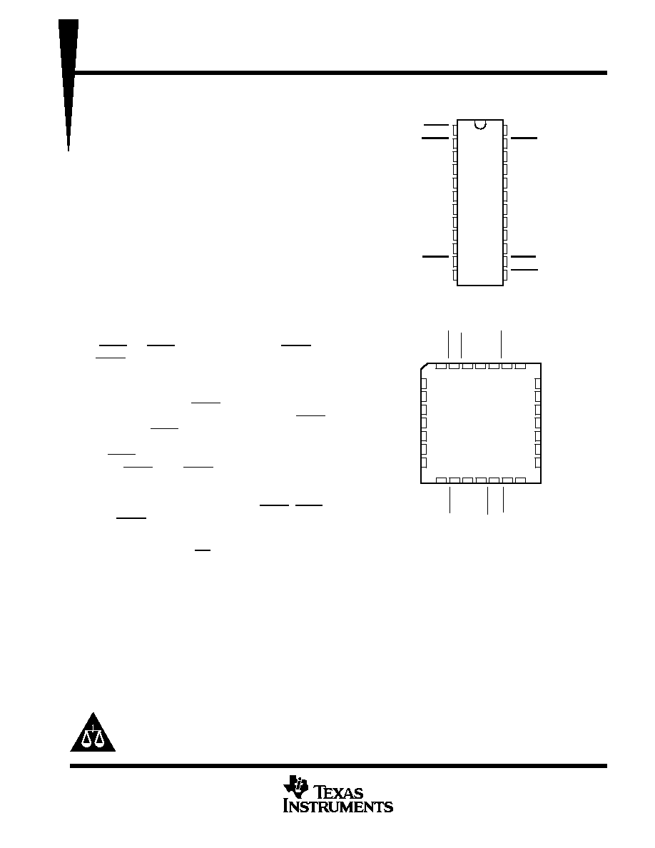
SN54ABT543A . . . JT OR W PACKAGE
SN74ABT543A . . . DB, DW, NT, OR PW PACKAGE
(TOP VIEW)
1
2
3
4
5
6
7
8
9
10
11
12
24
23
22
21
20
19
18
17
16
15
14
13
LEBA
OEBA
A1
A2
A3
A4
A5
A6
A7
A8
CEAB
GND
V
CC
CEBA
B1
B2
B3
B4
B5
B6
B7
B8
LEAB
OEAB
SN54ABT543A . . . FK PACKAGE
(TOP VIEW)
3 2 1 28 27
12 13
5
6
7
8
9
10
11
25
24
23
22
21
20
19
B2
B3
B4
NC
B5
B6
B7
A2
A3
A4
NC
A5
A6
A7
4
26
14 15 16 17 18
A8
CEAB
GND
NC
OEAB
LEAB
B8
A1
OEBA
LEBA
NC
CEBA
B1
V
CC
NC ≠ No internal connection
SN54ABT543A, SN74ABT543A
OCTAL REGISTERED TRANSCEIVERS
WITH 3-STATE OUTPUTS
SCBS157F ≠ JANUARY 1991 ≠ REVISED MAY 1997
2
POST OFFICE BOX 655303
∑
DALLAS, TEXAS 75265
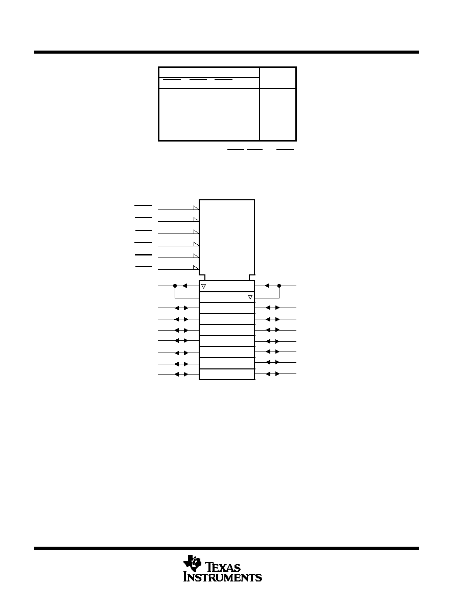
FUNCTION TABLE
INPUTS
OUTPUT
CEAB
LEAB
OEAB
A
B
H
X
X
X
Z
X
X
H
X
Z
L
H
L
X
B0
L
L
L
L
L
L
L
L
H
H
A-to-B data flow is shown; B-to-A flow control is the
same except that it uses CEBA, LEBA, and OEBA.
Output level before the indicated steady-state
input conditions were established
logic symbol
ß
4
2C6
14
3
A1
4
A2
B1
22
5D
5
A3
6
A4
7
A5
8
A6
9
A7
10
A8
B2
21
B3
20
B5
18
B4
19
B6
17
B8
15
B7
16
LEAB
3
G2
11
CEAB
2EN4
13
OEAB
1C5
1
LEBA
G1
23
CEBA
1EN3
2
OEBA
6D
ß This symbol is in accordance with ANSI/IEEE Std 91-1984 and IEC Publication 617-12.
Pin numbers shown are for the DB, DW, JT, NT, PW, and W packages.
1
1

SN54ABT543A, SN74ABT543A
OCTAL REGISTERED TRANSCEIVERS
WITH 3-STATE OUTPUTS
SCBS157F ≠ JANUARY 1991 ≠ REVISED MAY 1997
3
POST OFFICE BOX 655303
∑
DALLAS, TEXAS 75265
logic diagram (positive logic)
OEBA
CEBA
LEBA
OEAB
CEAB
LEAB
A1
B1
To Seven Other Channels
2
23
1
13
11
14
3
22
C1
1D
C1
1D
Pin numbers shown are for the DB, DW, JT, NT, PW, and W packages.
absolute maximum ratings over operating free-air temperature range (unless otherwise noted)
Supply voltage range, V
CC
≠0.5 V to 7 V
. . . . . . . . . . . . . . . . . . . . . . . . . . . . . . . . . . . . . . . . . . . . . . . . . . . . . . . . . .
Input voltage range, V
I
(except I/O ports) (see Note 1)
≠0.5 V to 7 V
. . . . . . . . . . . . . . . . . . . . . . . . . . . . . . . . . .
Voltage range applied to any output in the high or power-off state, V
O
≠0.5 V to 5.5 V
. . . . . . . . . . . . . . . . . . .
Current into any output in the low state, I
O
: SN54ABT543A 96
mA
. . . . . . . . . . . . . . . . . . . . . . . . . . . . . . . . . . .
SN74ABT543A
128 mA
. . . . . . . . . . . . . . . . . . . . . . . . . . . . . . . . . . .
Input clamp current, I
IK
(V
I
< 0)
≠18 mA
. . . . . . . . . . . . . . . . . . . . . . . . . . . . . . . . . . . . . . . . . . . . . . . . . . . . . . . . . . .
Output clamp current, I
OK
(V
O
< 0)
≠50 mA
. . . . . . . . . . . . . . . . . . . . . . . . . . . . . . . . . . . . . . . . . . . . . . . . . . . . . . . .
Package thermal impedance,
JA
(see Note 2): DB package
104
∞
C/W
. . . . . . . . . . . . . . . . . . . . . . . . . . . . . . . .
DW package
81
∞
C/W
. . . . . . . . . . . . . . . . . . . . . . . . . . . . . . . . .
NT package
67
∞
C/W
. . . . . . . . . . . . . . . . . . . . . . . . . . . . . . . . .
PW package
120
∞
C/W
. . . . . . . . . . . . . . . . . . . . . . . . . . . . . . . .
Storage temperature range, T
stg
≠65
∞
C to 150
∞
C
. . . . . . . . . . . . . . . . . . . . . . . . . . . . . . . . . . . . . . . . . . . . . . . . . . .
Stresses beyond those listed under "absolute maximum ratings" may cause permanent damage to the device. These are stress ratings only, and
functional operation of the device at these or any other conditions beyond those indicated under "recommended operating conditions" is not
implied. Exposure to absolute-maximum-rated conditions for extended periods may affect device reliability.
NOTES:
1. The input and output negative-voltage ratings may be exceeded if the input and output clamp-current ratings are observed.
2. The package thermal impedance is calculated in accordance with EIA/JEDEC Std JESD51, except for through-hole packages,
which use a trace length of zero.

SN54ABT543A, SN74ABT543A
OCTAL REGISTERED TRANSCEIVERS
WITH 3-STATE OUTPUTS
SCBS157F ≠ JANUARY 1991 ≠ REVISED MAY 1997
4
POST OFFICE BOX 655303
∑
DALLAS, TEXAS 75265
recommended operating conditions (see Note 3)
SN54ABT543A
SN74ABT543A
UNIT
MIN
MAX
MIN
MAX
UNIT
VCC
Supply voltage
4.5
5.5
4.5
5.5
V
VIH
High-level input voltage
2
2
V
VIL
Low-level input voltage
0.8
0.8
V
VI
Input voltage
0
VCC
0
VCC
V
IOH
High-level output current
≠24
≠32
mA
IOL
Low-level output current
48
64
mA
t/
v
Input transition rise or fall rate
Outputs enabled
5
5
ns/V
TA
Operating free-air temperature
≠55
125
≠40
85
∞
C
NOTE 3: Unused pins (input or I/O) must be held high or low to prevent them from floating.
electrical characteristics over recommended operating free-air temperature range (unless
otherwise noted)
PARAMETER
TEST CONDITIONS
TA = 25
∞
C
SN54ABT543A
SN74ABT543A
UNIT
PARAMETER
TEST CONDITIONS
MIN
TYP
MAX
MIN
MAX
MIN
MAX
UNIT
VIK
VCC = 4.5 V,
II = ≠18 mA
≠1.2
≠1.2
≠1.2
V
VCC = 4.5 V,
IOH = ≠3 mA
2.5
2.5
2.5
VOH
VCC = 5 V,
IOH = ≠3 mA
3
3
3
V
VOH
VCC = 4 5 V
IOH = ≠24 mA
2
2
V
VCC = 4.5 V
IOH = ≠32 mA
2*
2
VOL
VCC = 4 5 V
IOL = 48 mA
0.55
0.55
V
VOL
VCC = 4.5 V
IOL = 64 mA
0.55*
0.55
V
Vhys
100
mV
II
Control inputs
VCC = 5 5 V
VI = VCC or GND
±
1
±
1
±
1
µ
A
II
A or B ports
VCC = 5.5 V,
VI = VCC or GND
±
100
±
100
±
100
µ
A
IOZH
VCC = 5.5 V,
VO = 2.7 V
10ß
10ß
10ß
µ
A
IOZL
VCC = 5.5 V,
VO = 0.5 V
≠10ß
≠10ß
≠10ß
µ
A
Ioff
VCC = 0,
VI or VO
4.5 V
±
100
±
100
µ
A
ICEX
VCC = 5.5 V,
VO = 5.5 V
Outputs high
50
50
50
µ
A
IO∂
VCC = 5.5 V,
VO = 2.5 V
≠50*
≠100
≠180*
≠50
≠200
≠50
≠180
mA
VCC = 5.5 V,
Outputs high
1
250*
350
250
µ
A
ICC
A or B ports
VCC = 5.5 V,
IO = 0,
Outputs low
24
30*
34
30
mA
VI = VCC or GND
Outputs disabled
0.5
250*
350
250
µ
A
ICC#
VCC = 5.5 V, One input at 3.4 V,
Other inputs at VCC or GND
1.5
1.5
1.5
mA
Ci
Control inputs
VI = 2.5 V or 0.5 V
4
pF
Cio
A or B ports
VO = 2.5 V or 0.5 V
7
pF
* On products compliant to MIL-PRF-38535, this parameter does not apply.
All typical values are at VCC = 5 V.
The parameters IOZH and IOZL include the input leakage current.
ß This data sheet limit may vary among suppliers.
∂ Not more than one output should be tested at a time, and the duration of the test should not exceed one second.
# This is the increase in supply current for each input that is at the specified TTL voltage level rather than VCC or GND.
SN54ABT543A, SN74ABT543A
OCTAL REGISTERED TRANSCEIVERS
WITH 3-STATE OUTPUTS
SCBS157F ≠ JANUARY 1991 ≠ REVISED MAY 1997
5
POST OFFICE BOX 655303
∑
DALLAS, TEXAS 75265
timing requirements over recommended ranges of supply voltage and operating free-air
temperature (unless otherwise noted) (see Figure 1)
SN54ABT543A
VCC = 5 V,
TA = 25
∞
C
MIN
MAX
UNIT
MIN
MAX
tw
Pulse duration, LEAB or LEBA low
3.5
3.5
ns
Data before LEAB or LEBA
High
2.5
2.5
t
Setup time
Data before LEAB or LEBA
Low
3
3
ns
tsu
Setup time
Data before CEAB or CEBA
High
2.5
2.5
ns
Data before CEAB or CEBA
Low
3
3
th
Hold time
Data after LEAB or LEBA
1
1
ns
th
Hold time
Data after CEAB or CEBA
1
1
ns
timing requirements over recommended ranges of supply voltage and operating free-air
temperature (unless otherwise noted) (see Figure 1)
SN74ABT543A
VCC = 5 V,
TA = 25
∞
C
MIN
MAX
UNIT
MIN
MAX
tw
Pulse duration, LEAB or LEBA low
3.5
3.5
ns
Data before LEAB or LEBA
High
3.5
3.5
t
Setup time
Data before LEAB or LEBA
Low
3
3
ns
tsu
Setup time
Data before CEAB or CEBA
High
3.5
3.5
ns
Data before CEAB or CEBA
Low
3
3
th
Hold time
Data after LEAB or LEBA
0.5
0.5
ns
th
Hold time
Data after CEAB or CEBA
0.5
0.5
ns