Äîêóìåíòàöèÿ è îïèñàíèÿ www.docs.chipfind.ru
SN54ABT273, SN74ABT273
OCTAL EDGE-TRIGGERED D-TYPE FLIP-FLOPS
WITH CLEAR
SCBS185B FEBRUARY 1991 REVISED JANUARY 1997
1
POST OFFICE BOX 655303
·
DALLAS, TEXAS 75265
D
State-of-the-Art
EPIC-
B
TM
BiCMOS Design
Significantly Reduces Power Dissipation
D
Latch-Up Performance Exceeds 500 mA Per
JEDEC Standard JESD-17
D
Typical V
OLP
(Output Ground Bounce) < 1 V
at V
CC
= 5 V, T
A
= 25
°
C
D
High-Drive Outputs (32-mA I
OH
, 64-mA I
OL
)
D
Package Options Include Plastic
Small-Outline (DW), Shrink Small-Outline
(DB), and Thin Shrink Small-Outline (PW)
Packages, Ceramic Chip Carriers (FK),
Plastic (N) and Ceramic (J) DIPs, and
Ceramic Flat (W) Package
description
The 'ABT273 are 8-bit positive-edge-triggered
D-type flip-flops with a direct clear (CLR) input.
They are particularly suitable for implementing
buffer and storage registers, shift registers, and
pattern generators.
Information at the data (D) inputs meeting the
setup time requirements is transferred to the
Q outputs on the positive-going edge of the clock
pulse. Clock triggering occurs at a particular
voltage level and is not directly related to the
transition time of the positive-going pulse. When
the clock (CLK) input is at either the high or low
level, the D input signal has no effect at the output.
The SN54ABT273 is characterized for operation over the full military temperature range of 55
°
C to 125
°
C. The
SN74ABT273 is characterized for operation from 40
°
C to 85
°
C.
FUNCTION TABLE
(each flip-flop)
INPUTS
OUTPUT
CLR
CLK
D
OUTPUT
Q
L
X
X
L
H
H
H
H
L
L
H
H or L
X
Q0
Copyright
©
1997, Texas Instruments Incorporated
PRODUCTION DATA information is current as of publication date.
Products conform to specifications per the terms of Texas Instruments
standard warranty. Production processing does not necessarily include
testing of all parameters.
Please be aware that an important notice concerning availability, standard warranty, and use in critical applications of
Texas Instruments semiconductor products and disclaimers thereto appears at the end of this data sheet.
EPIC-
B is a trademark of Texas Instruments Incorporated.
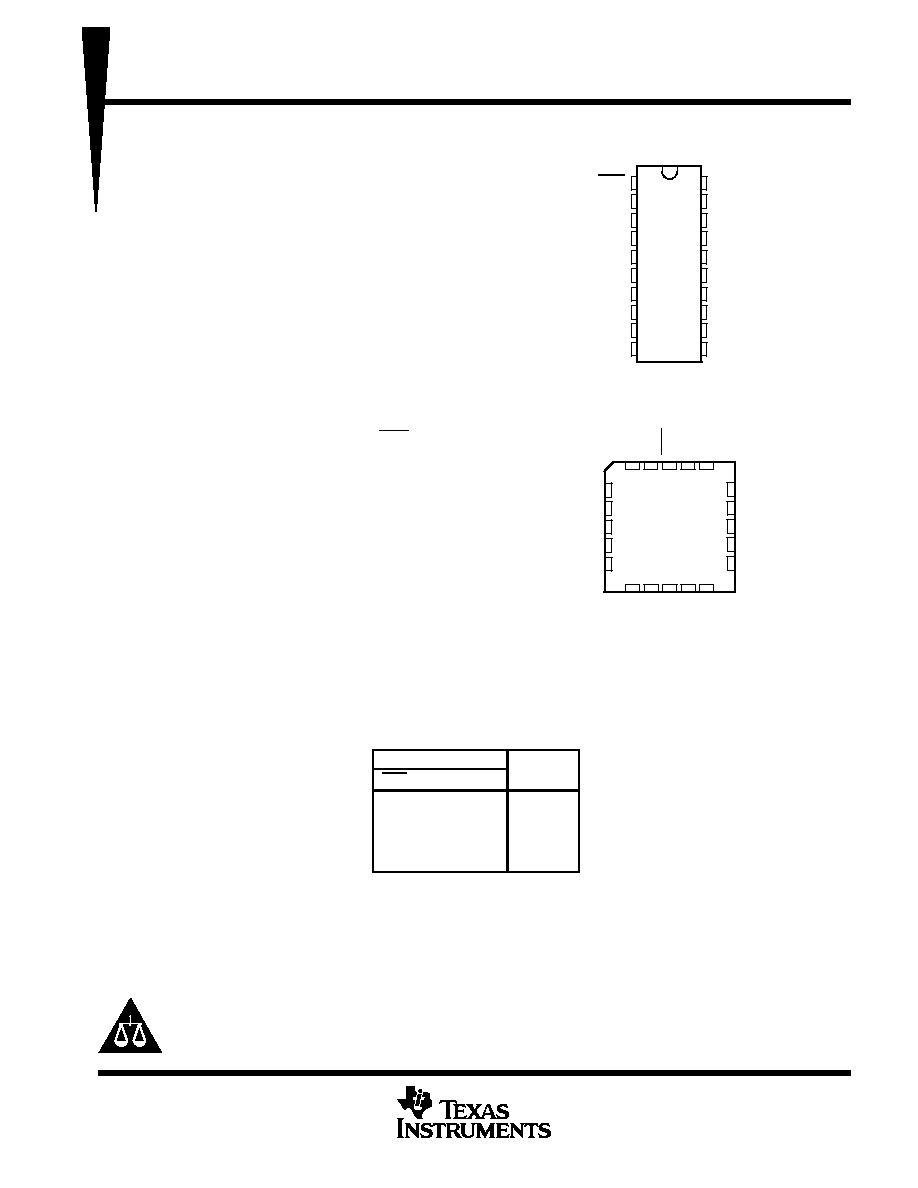
SN54ABT273 . . . J OR W PACKAGE
SN74ABT273 . . . DB, DW, N, OR PW PACKAGE
(TOP VIEW)
SN54ABT273 . . . FK PACKAGE
(TOP VIEW)
3
2
1 20 19
9 10 11 12 13
4
5
6
7
8
18
17
16
15
14
2D
2Q
3Q
3D
4D
1D
1Q
CLR
5Q
5D
8Q
4Q
GND
CLK
V
CC
8D
7D
7Q
6Q
6D
1
2
3
4
5
6
7
8
9
10
20
19
18
17
16
15
14
13
12
11
CLR
1Q
1D
2D
2Q
3Q
3D
4D
4Q
GND
V
CC
8Q
8D
7D
7Q
6Q
6D
5D
5Q
CLK
SN54ABT273, SN74ABT273
OCTAL EDGE-TRIGGERED D-TYPE FLIP-FLOPS
WITH CLEAR
SCBS185B FEBRUARY 1991 REVISED JANUARY 1997
2
POST OFFICE BOX 655303
·
DALLAS, TEXAS 75265
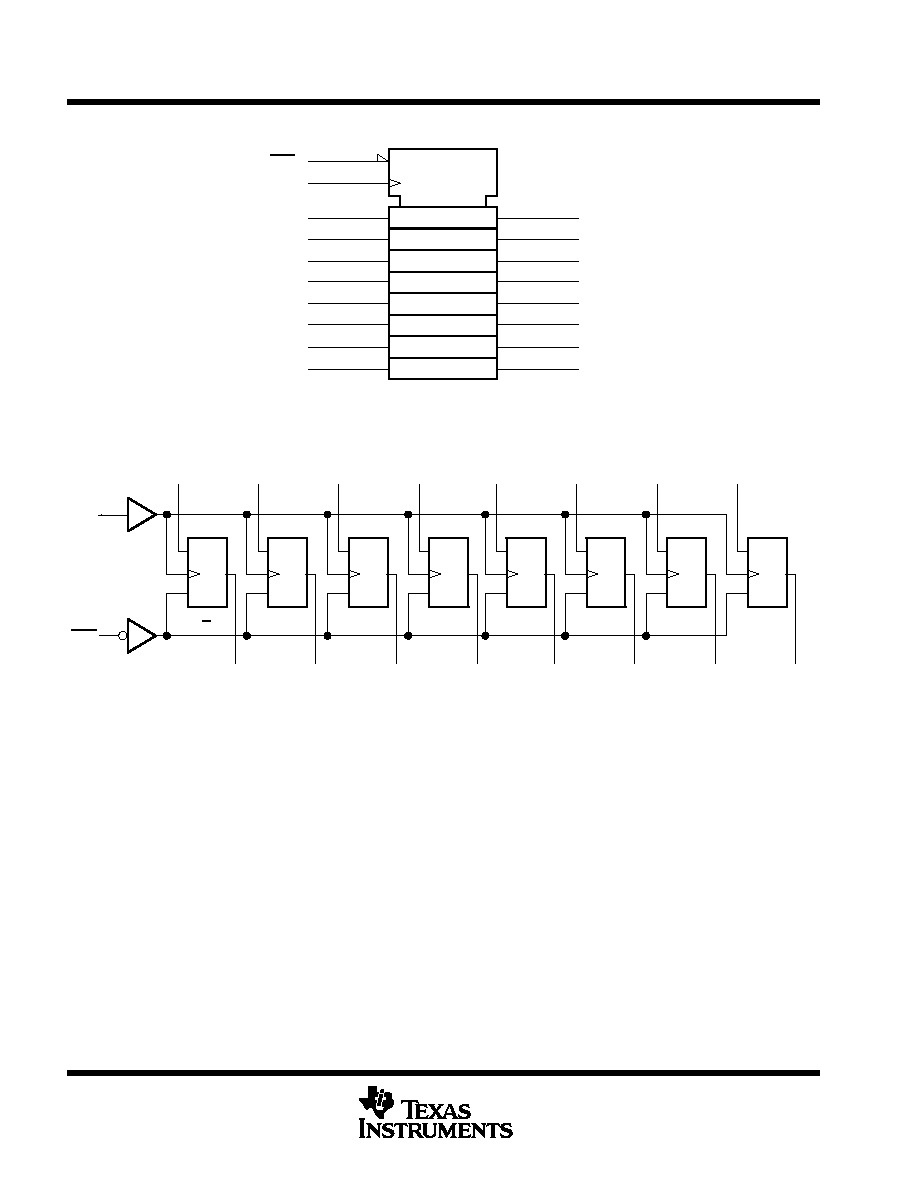
logic symbol
1D
3
1D
4
2D
7
3D
R
1
1Q
2
2Q
5
3Q
6
8
4D
13
5D
14
6D
4Q
9
5Q
12
6Q
15
CLR
17
7D
18
8D
11
CLK
7Q
16
8Q
19
C1
This symbol is in accordance with ANSI/IEEE Std 91-1984 and IEC Publication 617-12.
logic diagram (positive logic)
CLK
1D
3
1D
C1
R
1Q
2
2D
4
1D
C1
R
2Q
5
3D
7
1D
C1
R
3Q
6
4D
8
1D
C1
R
4Q
9
5D
13
1D
C1
R
5Q
12
6D
14
1D
C1
R
6Q
15
7D
17
1D
C1
R
7Q
16
8D
18
1D
C1
R
8Q
19
CLR
11
1
CLK(I)
R
absolute maximum ratings over operating free-air temperature range (unless otherwise noted)
Supply voltage range, V
CC
0.5 V to 7 V
. . . . . . . . . . . . . . . . . . . . . . . . . . . . . . . . . . . . . . . . . . . . . . . . . . . . . . . . . .
Input voltage range, V
I
(see Note 1)
0.5 V to 7 V
. . . . . . . . . . . . . . . . . . . . . . . . . . . . . . . . . . . . . . . . . . . . . . . . . .
Voltage range applied to any output in the high or power-off state, V
O
0.5 V to 5.5 V
. . . . . . . . . . . . . . . . . . .
Current into any output in the low state, I
O
: SN54ABT273 96
mA
. . . . . . . . . . . . . . . . . . . . . . . . . . . . . . . . . . . .
SN74ABT273 128
mA
. . . . . . . . . . . . . . . . . . . . . . . . . . . . . . . . . . .
Input clamp current, I
IK
(V
I
< 0)
18 mA
. . . . . . . . . . . . . . . . . . . . . . . . . . . . . . . . . . . . . . . . . . . . . . . . . . . . . . . . . . .
Output clamp current, I
OK
(V
O
< 0)
50 mA
. . . . . . . . . . . . . . . . . . . . . . . . . . . . . . . . . . . . . . . . . . . . . . . . . . . . . . . .
Package thermal impedance,
JA
(see Note 2): DB package
115
°
C/W
. . . . . . . . . . . . . . . . . . . . . . . . . . . . . . . .
DW package
97
°
C/W
. . . . . . . . . . . . . . . . . . . . . . . . . . . . . . . . .
N package
67
°
C/W
. . . . . . . . . . . . . . . . . . . . . . . . . . . . . . . . . . .
PW package
128
°
C/W
. . . . . . . . . . . . . . . . . . . . . . . . . . . . . . . .
Storage temperature range, T
stg
65
°
C to 150
°
C
. . . . . . . . . . . . . . . . . . . . . . . . . . . . . . . . . . . . . . . . . . . . . . . . . . .
Stresses beyond those listed under "absolute maximum ratings" may cause permanent damage to the device. These are stress ratings only, and
functional operation of the device at these or any other conditions beyond those indicated under "recommended operating conditions" is not
implied. Exposure to absolute-maximum-rated conditions for extended periods may affect device reliability.
NOTES:
1. The input and output negative-voltage ratings may be exceeded if the input and output clamp-current ratings are observed.
2. The package thermal impedance is calculated in accordance with EIA/JEDEC Std JESD51, except for through-hole packages,
which use a trace length of zero.
SN54ABT273, SN74ABT273
OCTAL EDGE-TRIGGERED D-TYPE FLIP-FLOPS
WITH CLEAR
SCBS185B FEBRUARY 1991 REVISED JANUARY 1997
3
POST OFFICE BOX 655303
·
DALLAS, TEXAS 75265
recommended operating conditions (see Note 3)
SN54ABT273
SN74ABT273
UNIT
MIN
MAX
MIN
MAX
UNIT
VCC
Supply voltage
4.5
5.5
4.5
5.5
V
VIH
High-level input voltage
2
2
V
VIL
Low-level input voltage
0.8
0.8
V
VI
Input voltage
0
VCC
0
VCC
V
IOH
High-level output current
24
32
mA
IOL
Low-level output current
48
64
mA
t/
v
Input transition rise or fall rate
10
10
ns/V
TA
Operating free-air temperature
55
125
40
85
°
C
NOTE 3: Unused inputs must be held high or low to prevent them from floating.
electrical characteristics over recommended operating free-air temperature range (unless
otherwise noted)
PARAMETER
TEST CONDITIONS
TA = 25
°
C
SN54ABT273
SN74ABT273
UNIT
PARAMETER
TEST CONDITIONS
MIN
TYP
MAX
MIN
MAX
MIN
MAX
UNIT
VIK
VCC = 4.5 V,
II = 18 mA
1.2
1.2
1.2
V
VCC = 4.5 V,
IOH = 3 mA
2.5
2.5
2.5
VOH
VCC = 5 V,
IOH = 3 mA
3
3
3
V
VOH
VCC = 4 5 V
IOH = 24 mA
2
2
V
VCC = 4.5 V
IOH = 32 mA
2*
2
VOL
VCC = 4 5 V
IOL = 48 mA
0.55
0.55
V
VOL
VCC = 4.5 V
IOL = 64 mA
0.55*
0.55
V
Vhys
100
mV
II
VCC = 5.5 V,
VI = VCC or GND
±
1
±
1
±
1
µ
A
Ioff
VCC = 0,
VI or VO
4.5 V
±
100
±
100
µ
A
ICEX
VCC = 5.5 V,
VO = 5.5 V
Outputs high
50
50
50
µ
A
IO
VCC = 5.5 V,
VO = 2.5 V
50
100
200§
50
200§
50
200§
mA
ICC
VCC = 5.5 V, IO = 0,
Outputs high
1
400§
400§
400§
µ
A
ICC
CC
, O
,
VI = VCC or GND
Outputs low
24
30
30
30
mA
ICC¶
VCC = 5.5 V, One input at 3.4 V,
Other inputs at VCC or GND
1.5
1.5
1.5
mA
Ci
VI = 2.5 V or 0.5 V
7
pF
* On products compliant to MIL-PRF-38535, this parameter does not apply.
All typical values are at VCC = 5 V.
Not more than one output should be tested at a time, and the duration of the test should not exceed one second.
§ This data sheet limit may vary among suppliers.
¶ This is the increase in supply current for each input that is at the specified TTL voltage level rather than VCC or GND.
SN54ABT273, SN74ABT273
OCTAL EDGE-TRIGGERED D-TYPE FLIP-FLOPS
WITH CLEAR
SCBS185B FEBRUARY 1991 REVISED JANUARY 1997
4
POST OFFICE BOX 655303
·
DALLAS, TEXAS 75265
timing requirements over recommended ranges of supply voltage and operating free-air
temperature (unless otherwise noted) (see Figure 1)
VCC = 5 V,
TA = 25
°
C
SN54ABT273
SN74ABT273
UNIT
MIN
MAX
MIN
MAX
MIN
MAX
fclock
Clock frequency
0
150
0
150
0
150
MHz
t
Pulse duration
CLK high or low
3.3
3.3
3.3
ns
tw
Pulse duration
CLR low
3.3
3.3
3.3
ns
Data high
2
2
2
tsu
Setup time before CLK
Data low
2.5
2.5
2.5
ns
CLR high
2
2
2
th
Hold time after CLK
Data high or low
1.2
1.4
1.2
ns
This data sheet limit may vary among suppliers.
switching characteristics over recommended ranges of supply voltage and operating free-air
temperature, C
L
= 50 pF (unless otherwise noted) (see Figure 1)
PARAMETER
FROM
(INPUT)
TO
(OUTPUT)
VCC = 5 V,
TA = 25
°
C
SN54ABT273
UNIT
(INPUT)
(OUTPUT)
MIN
MAX
MIN
MAX
fmax
150
150
MHz
tPLH
CLK
Q
2.5
6
2.5
7
ns
tPHL
CLK
Q
3.3
6.8
3.3
7.5
ns
tPHL
CLR
Q
2.5
7.5
2.5
8.2
ns
This data sheet limit may vary among suppliers.
switching characteristics over recommended ranges of supply voltage and operating free-air
temperature, C
L
= 50 pF (unless otherwise noted) (see Figure 1)
PARAMETER
FROM
(INPUT)
TO
(OUTPUT)
VCC = 5 V,
TA = 25
°
C
SN74ABT273
UNIT
(INPUT)
(OUTPUT)
MIN
MAX
MIN
MAX
fmax
150
150
MHz
tPLH
CLK
Q
2.5
6
2.5
6.5
ns
tPHL
CLK
Q
3.3
6.8
3.3
7.3
ns
tPHL
CLR
Q
2.5
6.7
2.5
7.4
ns
This data sheet limit may vary among suppliers.
SN54ABT273, SN74ABT273
OCTAL EDGE-TRIGGERED D-TYPE FLIP-FLOPS
WITH CLEAR
SCBS185B FEBRUARY 1991 REVISED JANUARY 1997
5
POST OFFICE BOX 655303
·
DALLAS, TEXAS 75265
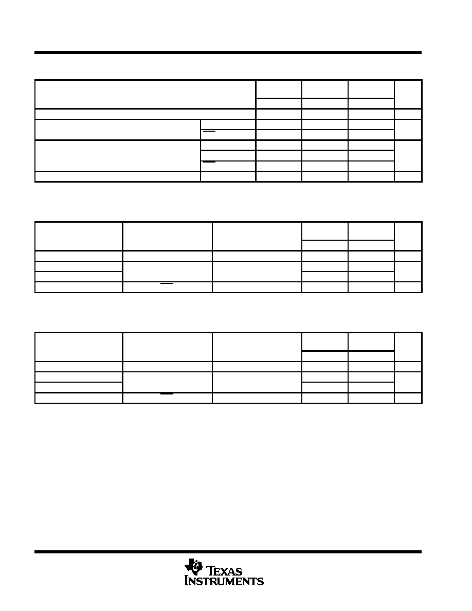
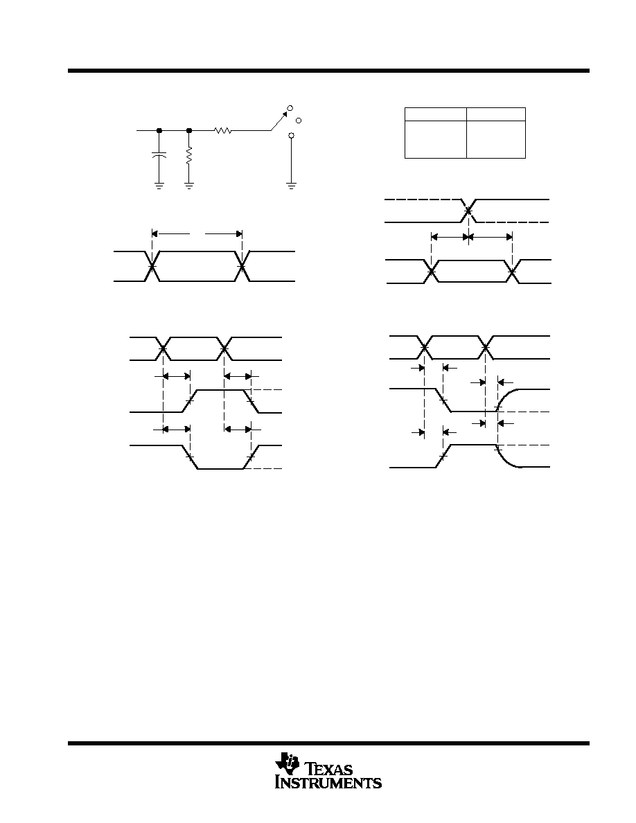
PARAMETER MEASUREMENT INFORMATION
1.5 V
th
tsu
From Output
Under Test
CL = 50 pF
(see Note A)
LOAD CIRCUIT
S1
7 V
Open
GND
500
500
Data Input
Timing Input
1.5 V
3 V
0 V
1.5 V
1.5 V
3 V
0 V
3 V
0 V
1.5 V
tw
Input
VOLTAGE WAVEFORMS
SETUP AND HOLD TIMES
VOLTAGE WAVEFORMS
PROPAGATION DELAY TIMES
INVERTING AND NONINVERTING OUTPUTS
VOLTAGE WAVEFORMS
PULSE DURATION
tPLH
tPHL
tPHL
tPLH
VOH
VOH
VOL
VOL
1.5 V
1.5 V
3 V
0 V
1.5 V
1.5 V
Input
1.5 V
Output
Control
Output
Waveform 1
S1 at 7 V
(see Note B)
Output
Waveform 2
S1 at Open
(see Note B)
VOL
VOH
tPZL
tPZH
tPLZ
tPHZ
1.5 V
1.5 V
3.5 V
0 V
1.5 V
VOL + 0.3 V
1.5 V
VOH 0.3 V
0 V
3 V
VOLTAGE WAVEFORMS
ENABLE AND DISABLE TIMES
LOW- AND HIGH-LEVEL ENABLING
Output
Output
tPLH/tPHL
tPLZ/tPZL
tPHZ/tPZH
Open
7 V
Open
TEST
S1
Output
Control
NOTES: A. CL includes probe and jig capacitance.
B. Waveform 1 is for an output with internal conditions such that the output is low except when disabled by the output control.
Waveform 2 is for an output with internal conditions such that the output is high except when disabled by the output control.
C. All input pulses are supplied by generators having the following characteristics: PRR
10 MHz, ZO = 50
, tr
2.5 ns, tf
2.5 ns.
D. The outputs are measured one at a time with one transition per measurement.
1.5 V
Figure 1. Load Circuit and Voltage Waveforms