SN54ABT573, SN74ABT573A
OCTAL TRANSPARENT D TYPE LATCHES
WITH 3 STATE OUTPUTS
SCBS190F - JANUARY 1991 - REVISED SEPTEMBER 2003
1
POST OFFICE BOX 655303
∑
DALLAS, TEXAS 75265
D
Typical V
OLP
(Output Ground Bounce)
<1 V at V
CC
= 5 V, T
A
= 25
∞
C
D
High-Drive Outputs (-32-mA I
OH
, 64-mA I
OL
)
D
I
off
Supports Partial-Power-Down Mode
Operation
D
Latch-Up Performance Exceeds 500 mA Per
JEDEC Standard JESD 17
D
ESD Protection Exceeds JESD 22
- 2000-V Human-Body Model (A114-A)
- 200-V Machine Model (A115-A)
1
2
3
4
5
6
7
8
9
10
20
19
18
17
16
15
14
13
12
11
OE
1D
2D
3D
4D
5D
6D
7D
8D
GND
V
CC
1Q
2Q
3Q
4Q
5Q
6Q
7Q
8Q
LE
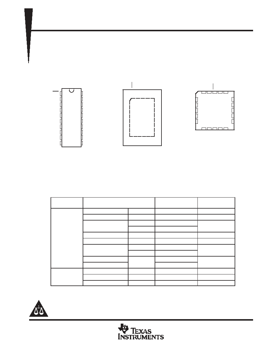
SN54ABT573 . . . J OR W PACKAGE
SN74ABT573A . . . DB, DW, N, NS,
OR PW PACKAGE
(TOP VIEW)
3
2
1 20 19
9 10 11 12 13
4
5
6
7
8
18
17
16
15
14
2Q
3Q
4Q
5Q
6Q
3D
4D
5D
6D
7D
SN54ABT573 . . . FK PACKAGE
(TOP VIEW)
2D
1D
OE
8Q
7Q
1Q
8D
GND
LE
V
CC
SN74ABT573A . . . RGY PACKAGE
(TOP VIEW)
1
20
10
11
2
3
4
5
6
7
8
9
19
18
17
16
15
14
13
12
1Q
2Q
3Q
4Q
5Q
6Q
7Q
8Q
1D
2D
3D
4D
5D
6D
7D
8D
LE
V
GND
CC
OE
description/ordering information
These 8-bit latches feature 3-state outputs designed specifically for driving highly capacitive or relatively
low-impedance loads. They are particularly suitable for implementing buffer registers, I/O ports, bidirectional
bus drivers, and working registers.
ORDERING INFORMATION
TA
PACKAGE
ORDERABLE
PART NUMBER
TOP-SIDE
MARKING
PDIP - N
Tube
SN74ABT573AN
SN74ABT573AN
QFN - RGY
Tape and reel
SN74ABT573ARGYR
AB573A
SOIC - DW
Tube
SN74ABT573ADW
ABT573A
SOIC - DW
Tape and reel
SN74ABT573ADWR
ABT573A
-40
∞
C to 85
∞
C
SOP - NS
Tape and reel
SN74ABT573ANSR
ABT573A
-40
∞
C to 85
∞
C
SSOP - DB
Tape and reel
SN74ABT573ADBR
AB573A
TSSOP - PW
Tube
SN74ABT573APW
AB573A
TSSOP - PW
Tape and reel
SN74ABT573APWR
AB573A
VFBGA - GQN
Tape and reel
SN74ABT573AGQNR
AB573A
VFBGA - ZQN (Pb-free)
Tape and reel
SN74ABT573AZQNR
AB573A
CDIP - J
Tube
SNJ54ABT573J
SNJ54ABT573J
-55
∞
C to 125
∞
C
CFP - W
Tube
SNJ54ABT573W
SNJ54ABT573W
-55 C to 125 C
LCCC - FK
Tube
SNJ54ABT573FK
SNJ54ABT573FK
Package drawings, standard packing quantities, thermal data, symbolization, and PCB design guidelines
are available at www.ti.com/sc/package.
Copyright
2003, Texas Instruments Incorporated
PRODUCTION DATA information is current as of publication date.
Products conform to specifications per the terms of Texas Instruments
standard warranty. Production processing does not necessarily include
testing of all parameters.
Please be aware that an important notice concerning availability, standard warranty, and use in critical applications of
Texas Instruments semiconductor products and disclaimers thereto appears at the end of this data sheet.
On products compliant to MIL PRF 38535, all parameters are tested
unless otherwise noted. On all other products, production
processing does not necessarily include testing of all parameters.
SN54ABT573, SN74ABT573A
OCTAL TRANSPARENT D TYPE LATCHES
WITH 3 STATE OUTPUTS
SCBS190F - JANUARY 1991 - REVISED SEPTEMBER 2003
2
POST OFFICE BOX 655303
∑
DALLAS, TEXAS 75265
description/ordering information (continued)
A buffered output-enable (OE) input can be used to place the eight outputs in either a normal logic state (high
or low logic levels) or the high-impedance state. In the high-impedance state, the outputs neither load nor drive
the bus lines significantly. The high-impedance state and increased drive provide the capability to drive bus
lines without need for interface or pullup components.
OE does not affect the internal operations of the latches. Old data can be retained or new data can be entered
while the outputs are in the high-impedance state.
To ensure the high-impedance state during power up or power down, OE should be tied to V
CC
through a pullup
resistor; the minimum value of the resistor is determined by the current-sinking capability of the driver.
This device is fully specified for partial-power-down applications using I
off
. The I
off
circuitry disables the outputs,
preventing damaging current backflow through the device when it is powered down.
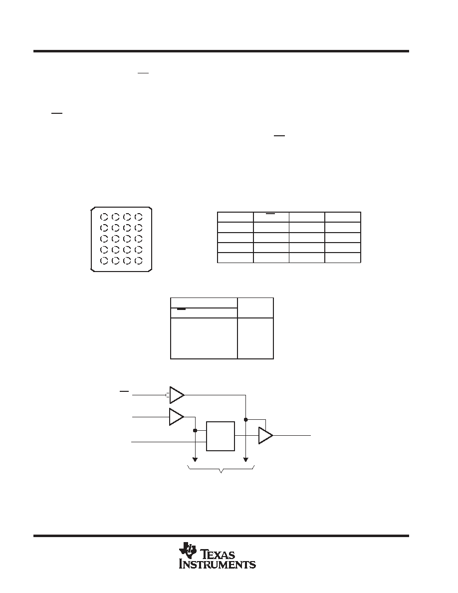
terminal assignments
1
2
3
4
A
1D
OE
VCC
1Q
B
3D
3Q
2D
2Q
C
5D
4D
5Q
4Q
D
7D
7Q
6D
6Q
E
GND
8D
LE
8Q
FUNCTION TABLE
(each latch)
INPUTS
OUTPUT
OE
LE
D
OUTPUT
Q
L
H
H
H
L
H
L
L
L
L
X
Q0
H
X
X
Z
logic diagram (positive logic)
OE
To Seven Other Channels
1
11
2
19
LE
1D
C1
1D
1Q
Pin numbers shown are for the DB, DW, FK, J, N, NS, PW, RGY, and W packages.
SN74ABT573A . . . GQN OR ZQN PACKAGE
(TOP VIEW)
1
2
3
4
A
B
C
D
E
SN54ABT573, SN74ABT573A
OCTAL TRANSPARENT D TYPE LATCHES
WITH 3 STATE OUTPUTS
SCBS190F - JANUARY 1991 - REVISED SEPTEMBER 2003
3
POST OFFICE BOX 655303
∑
DALLAS, TEXAS 75265
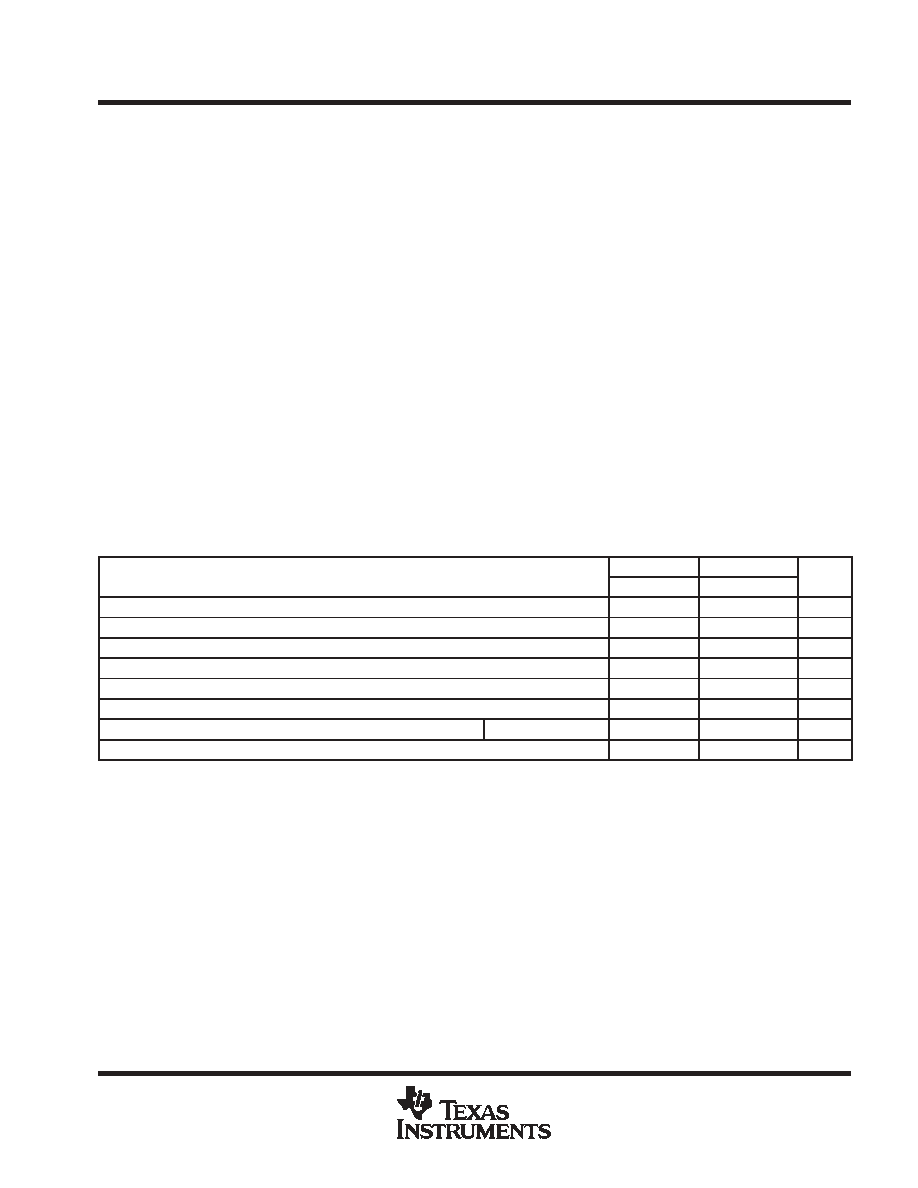
absolute maximum ratings over operating free-air temperature range (unless otherwise noted)
Supply voltage range, V
CC
-0.5 V to 7 V
. . . . . . . . . . . . . . . . . . . . . . . . . . . . . . . . . . . . . . . . . . . . . . . . . . . . . . . . . .
Input voltage range, V
I
(see Note 1)
-0.5 V to 7 V
. . . . . . . . . . . . . . . . . . . . . . . . . . . . . . . . . . . . . . . . . . . . . . . . . .
Voltage range applied to any output in the high or power-off state, V
O
-0.5 V to 5.5 V
. . . . . . . . . . . . . . . . . . .
Current into any output in the low state, I
O
: SN54ABT573 96
mA
. . . . . . . . . . . . . . . . . . . . . . . . . . . . . . . . . . . .
SN74ABT573A 128
mA
. . . . . . . . . . . . . . . . . . . . . . . . . . . . . . . . . .
Input clamp current, I
IK
(V
I
< 0)
-18 mA
. . . . . . . . . . . . . . . . . . . . . . . . . . . . . . . . . . . . . . . . . . . . . . . . . . . . . . . . . . .
Output clamp current, I
OK
(V
O
< 0)
-50 mA
. . . . . . . . . . . . . . . . . . . . . . . . . . . . . . . . . . . . . . . . . . . . . . . . . . . . . . . .
Package thermal impedance,
JA
(see Note 2): DB package
70
∞
C/W
. . . . . . . . . . . . . . . . . . . . . . . . . . . . . . . . .
(see Note 2): DW package
58
∞
C/W
. . . . . . . . . . . . . . . . . . . . . . . . . . . . . . . . .
(see Note 2): GQN/ZQN package
78
∞
C/W
. . . . . . . . . . . . . . . . . . . . . . . . . . .
(see Note 2): N package
69
∞
C/W
. . . . . . . . . . . . . . . . . . . . . . . . . . . . . . . . . . .
(see Note 2): NS package
60
∞
C/W
. . . . . . . . . . . . . . . . . . . . . . . . . . . . . . . . .
(see Note 2): PW package
83
∞
C/W
. . . . . . . . . . . . . . . . . . . . . . . . . . . . . . . . .
(see Note 3): RGY package
37
∞
C/W
. . . . . . . . . . . . . . . . . . . . . . . . . . . . . . . .
Storage temperature range, T
stg
-65
∞
C to 150
∞
C
. . . . . . . . . . . . . . . . . . . . . . . . . . . . . . . . . . . . . . . . . . . . . . . . . . .
Stresses beyond those listed under "absolute maximum ratings" may cause permanent damage to the device. These are stress ratings only, and
functional operation of the device at these or any other conditions beyond those indicated under "recommended operating conditions" is not
implied. Exposure to absolute-maximum-rated conditions for extended periods may affect device reliability.
NOTES:
1. The input and output negative-voltage ratings may be exceeded if the input and output clamp-current ratings are observed.
2. The package thermal impedance is calculated in accordance with JESD 51-7.
3. The package thermal impedance is calculated in accordance with JESD 51-5.
recommended operating conditions (see Note 4)
SN54ABT573
SN74ABT573A
UNIT
MIN
MAX
MIN
MAX
UNIT
VCC
Supply voltage
4.5
5.5
4.5
5.5
V
VIH
High-level input voltage
2
2
V
VIL
Low-level input voltage
0.8
0.8
V
VI
Input voltage
0
VCC
0
VCC
V
IOH
High-level output current
-24
-32
mA
IOL
Low-level output current
48
64
mA
t/
v
Input transition rise or fall rate
Outputs enabled
5
5
ns/V
TA
Operating free-air temperature
-55
125
-40
85
∞
C
NOTE 4: All unused inputs of the device must be held at VCC or GND to ensure proper device operation. Refer to the TI application report,
Implications of Slow or Floating CMOS Inputs, literature number SCBA004.
SN54ABT573, SN74ABT573A
OCTAL TRANSPARENT D TYPE LATCHES
WITH 3 STATE OUTPUTS
SCBS190F - JANUARY 1991 - REVISED SEPTEMBER 2003
4
POST OFFICE BOX 655303
∑
DALLAS, TEXAS 75265
electrical characteristics over recommended operating free-air temperature range (unless
otherwise noted)
PARAMETER
TEST CONDITIONS
TA = 25
∞
C
SN54ABT573
SN74ABT573A
UNIT
PARAMETER
TEST CONDITIONS
MIN
TYP
MAX
MIN
MAX
MIN
MAX
UNIT
VIK
VCC = 4.5 V,
II = -18 mA
-1.2
-1.2
-1.2
V
VCC = 4.5 V,
IOH = -3 mA
2.5
2.5
2.5
VOH
VCC = 5 V,
IOH = -3 mA
3
3
3
V
VOH
VCC = 4.5 V
IOH = -24 mA
2
2
V
VCC = 4.5 V
IOH = -32 mA
2*
2
VOL
VCC = 4.5 V
IOL = 48 mA
0.55
0.55
V
VOL
VCC = 4.5 V
IOL = 64 mA
0.55*
0.55
V
Vhys
100
mV
II
VCC = 5.5 V,
VI = VCC or GND
±
1
±
1
±
1
µ
A
IOZH
VCC = 5.5 V,
VO = 2.7 V
10
10
10
µ
A
IOZL
VCC = 5.5 V,
VO = 0.5 V
-10
-10
-10
µ
A
Ioff
VCC = 0,
VI or VO
4.5 V
±
100
±
100
µ
A
ICEX
VCC = 5.5 V,
VO = 5.5 V
Outputs high
50
50
50
µ
A
IOß
VCC = 5.5 V,
VO = 2.5 V
-50
-100
-180
-50
-180
-50
-180
mA
VCC = 5.5 V, IO = 0,
Outputs high
1
250
250
250
µ
A
ICC
VCC = 5.5 V, IO = 0,
VI = VCC or GND
Outputs low
24
30
30
30
mA
ICC
VI = VCC or GND
Outputs disabled
0.5
250
250
250
µ
A
ICC∂
VCC = 5.5 V, One input at 3.4 V,
Other inputs at VCC or GND
1.5
1.5
1.5
mA
Ci
VI = 2.5 V or 0.5 V
3.5
pF
Co
VO = 2.5 V or 0.5 V
6.5
pF
* On products compliant to MIL-PRF-38535, this parameter does not apply.
All typical values are at VCC = 5 V.
This data sheet limit may vary among suppliers.
ß Not more than one output should be tested at a time, and the duration of the test should not exceed one second.
∂ This is the increase in supply current for each input that is at the specified TTL voltage level, rather than VCC or GND.
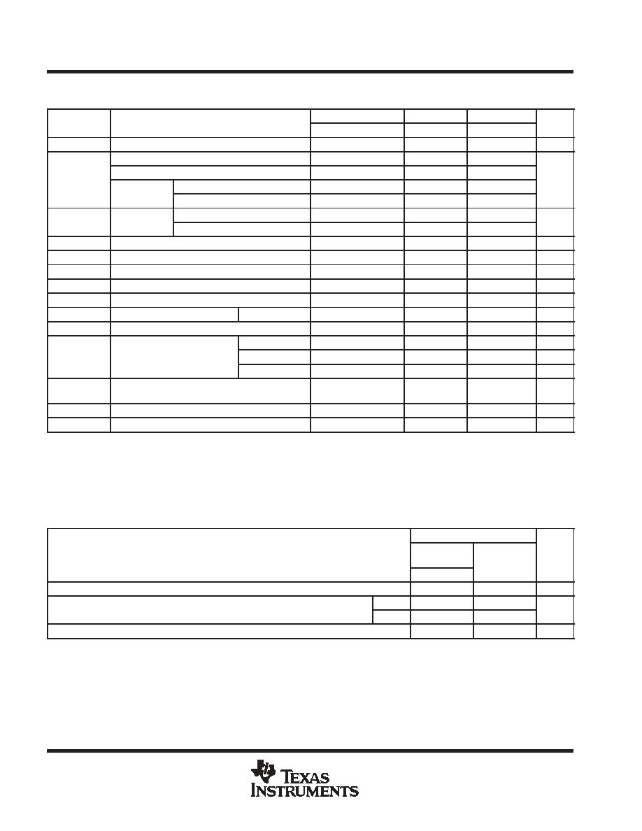
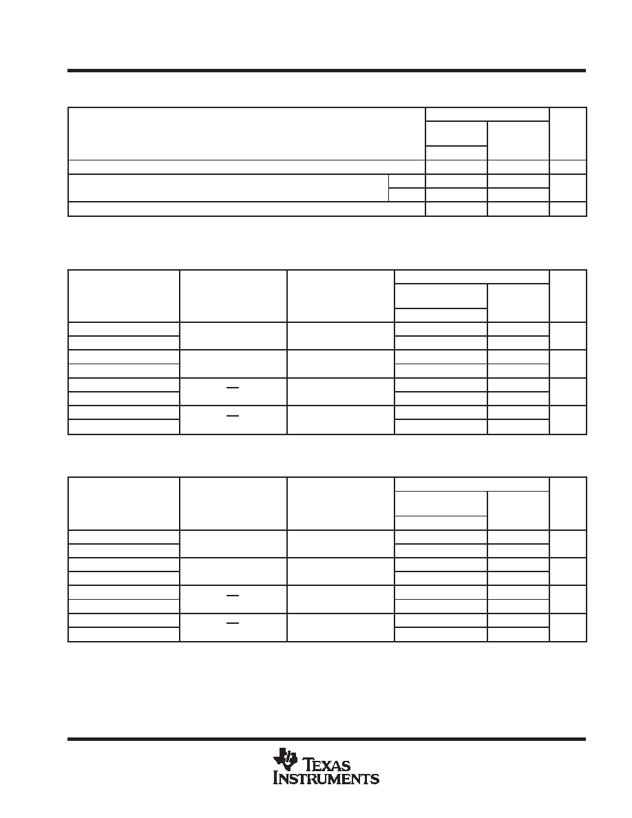
timing requirements over recommended ranges of supply voltage and operating free-air
temperature (unless otherwise noted) (see Figure 1)
SN54ABT573
VCC = 5 V,
TA = 25
∞
C
MIN
MAX
UNIT
MIN
MAX
MIN
MAX
tw
Pulse duration, LE high
3.3
3.3
ns
tsu
Setup time, data before LE
High
1.9
2.5
ns
tsu
Setup time, data before LE
Low
1.5
2.5
ns
th
Hold time, data after LE
1
2.5
ns
SN54ABT573, SN74ABT573A
OCTAL TRANSPARENT D TYPE LATCHES
WITH 3 STATE OUTPUTS
SCBS190F - JANUARY 1991 - REVISED SEPTEMBER 2003
5
POST OFFICE BOX 655303
∑
DALLAS, TEXAS 75265
timing requirements over recommended ranges of supply voltage and operating free-air
temperature (unless otherwise noted) (see Figure 1)
SN74ABT573A
VCC = 5 V,
TA = 25
∞
C
MIN
MAX
UNIT
MIN
MAX
MIN
MAX
tw
Pulse duration, LE high
3.3
3.3
ns
tsu
Setup time, data before LE
High
1.9
1.9
ns
tsu
Setup time, data before LE
Low
1.5
1.5
ns
th
Hold time, data after LE
1.8
1.8
ns
This data-sheet limit may vary among suppliers.
switching characteristics over recommended ranges of supply voltage and operating free-air
temperature, C
L
= 50 pF (unless otherwise noted) (see Figure 1)
SN54ABT573
PARAMETER
FROM
(INPUT)
TO
(OUTPUT)
VCC = 5 V,
TA = 25
∞
C
MIN
MAX
UNIT
(INPUT)
(OUTPUT)
MIN
TYP
MAX
MIN
MAX
tPLH
D
Q
1.9
3.2
5.4
1.4
6.4
ns
tPHL
D
Q
2.2
4.2
5.7
1.6
6.7
ns
tPLH
LE
Q
2.2
4
6.1
2
7.1
ns
tPHL
LE
Q
3.2
5.2
6.7
2.8
7.5
ns
tPZH
OE
Q
1.2
3.2
4.7
0.8
6.2
ns
tPZL
OE
Q
2.7
4.7
6.2
2
7.2
ns
tPHZ
OE
Q
2.5
4.9
6.4
2.2
7.7
ns
tPLZ
OE
Q
2
4.2
6
1.4
7
ns
switching characteristics over recommended ranges of supply voltage and operating free-air
temperature, C
L
= 50 pF (unless otherwise noted) (see Figure 1)
SN74ABT573A
PARAMETER
FROM
(INPUT)
TO
(OUTPUT)
VCC = 5 V,
TA = 25
∞
C
MIN
MAX
UNIT
(INPUT)
(OUTPUT)
MIN
TYP
MAX
MIN
MAX
tPLH
D
Q
1.9
3.2
5.4
1.9
5.9
ns
tPHL
D
Q
2.2
4.2
5.7
2.2
6.2
ns
tPLH
LE
Q
2.2
4
6.1
2.2
6.6
ns
tPHL
LE
Q
3.2
5.2
6.7
3.2
7.2
ns
tPZH
OE
Q
1.2
3.2
4.7
1.2
5.2
ns
tPZL
OE
Q
2.5
4.7
6.2
2.5
6.7
ns
tPHZ
OE
Q
2.5
4.9
6.4
2.5
7.1
ns
tPLZ
OE
Q
2
4.2
6
2
6.5
ns
This data-sheet limit may vary among suppliers.