SN54ABT2244, SN74ABT2244
OCTAL BUFFERS AND LINE/MOS DRIVERS
WITH 3-STATE OUTPUTS
SCBS106B ≠ JANUARY 1991 ≠ REVISED JULY 1994
Copyright
©
1994, Texas Instruments Incorporated
6≠1
POST OFFICE BOX 655303
∑
DALLAS, TEXAS 75265
∑
Output Ports Have Equivalent 25-
Series
Resistors, So No External Resistors Are
Required
∑
State-of-the-Art
EPIC-
B
TM
BiCMOS Design
Significantly Reduces Power Dissipation
∑
Typical V
OLP
(Output Ground Bounce)
< 1 V at V
CC
= 5 V, T
A
= 25
∞
C
∑
Package Options Include Plastic
Small-Outline (DW), Shrink Small-Outline
(DB), and Thin Shrink Small-Outline (PW)
Packages, Ceramic Chip Carriers (FK), and
Plastic (N) and Ceramic (J) DIPs
description
These octal buffers and line drivers are designed
specifically to improve both the performance and
density of 3-state memory address drivers, clock
drivers, and bus-oriented receivers and
transmitters. Taken together with the
ABT2240
and
ABT2241, these devices provide the choice
of selected combinations of inverting and
noninverting outputs, symmetrical active-low
output-enable (OE) inputs, and complementary
OE and OE inputs. These devices feature high
fan-out and improved fan-in.
The outputs, which are designed to sink up to
12 mA, include 25-
series resistors to reduce
overshoot and undershoot.
To ensure the high-impedance state during power up or power down, OE should be tied to V
CC
through a pullup
resistor; the minimum value of the resistor is determined by the current-sinking capability of the driver.
The SN74ABT2244 is available in TI's shrink small-outline package (DB), which provides the same I/O pin count
and functionality of standard small-outline packages in less than half the printed-circuit-board area.
The SN54ABT2244 is characterized for operation over the full military temperature range of ≠ 55
∞
C to 125
∞
C.
The SN74ABT2244 is characterized for operation from ≠ 40
∞
C to 85
∞
C.
FUNCTION TABLE
(each buffer)
INPUTS
OUTPUT
OE
A
Y
L
H
H
L
L
L
H
X
Z
1
2
3
4
5
6
7
8
9
10
20
19
18
17
16
15
14
13
12
11
1OE
1A1
2Y4
1A2
2Y3
1A3
2Y2
1A4
2Y1
GND
V
CC
2OE
1Y1
2A4
1Y2
2A3
1Y3
2A2
1Y4
2A1
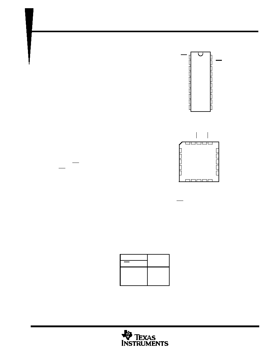
SN54ABT2244 . . . J PACKAGE
SN74ABT2244 . . . DB, DW, N, OR PW PACKAGE
(TOP VIEW)
3
2
1 20 19
9 10 11 12 13
4
5
6
7
8
18
17
16
15
14
1Y1
2A4
1Y2
2A3
1Y3
1A2
2Y3
1A3
2Y2
1A4
SN54ABT2244 . . . FK PACKAGE
(TOP VIEW)
2Y4
1A1
1OE
1Y4
2A2
2OE
2Y1
GND
2A1
V
CC
EPIC-
B is a trademark of Texas Instruments Incorporated.
PRODUCTION DATA information is current as of publication date.
Products conform to specifications per the terms of Texas Instruments
standard warranty. Production processing does not necessarily include
testing of all parameters.
SN54ABT2244, SN74ABT2244
OCTAL BUFFERS AND LINE/MOS DRIVERS
WITH 3-STATE OUTPUTS
SCBS106B ≠ JANUARY 1991 ≠ REVISED JULY 1994
6≠2
POST OFFICE BOX 655303
∑
DALLAS, TEXAS 75265
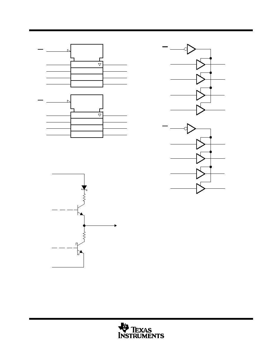
logic symbol
logic diagram (positive logic)
1OE
2
1A1
4
1A2
6
1A3
8
1A4
EN
1
1Y1
18
1Y2
16
1Y3
14
1Y4
12
2OE
11
2A1
13
2A2
15
2A3
17
2A4
EN
19
2Y1
9
2Y2
7
2Y3
5
2Y4
3
1
2
4
6
8
19
11
13
15
17
3
5
7
9
12
14
16
18
1A1
1A2
1A3
1A4
1Y1
2A1
2A2
2A3
2A4
2Y1
1Y2
1Y3
1Y4
2Y2
2Y3
2Y4
1OE
2OE
This symbol is in accordance with ANSI/IEEE Std 91-1984
and IEC Publication 617-12.
schematic of Y outputs
Output
VCC
GND
1
1
SN54ABT2244, SN74ABT2244
OCTAL BUFFERS AND LINE/MOS DRIVERS
WITH 3-STATE OUTPUTS
SCBS106B ≠ JANUARY 1991 ≠ REVISED JULY 1994
6≠3
POST OFFICE BOX 655303
∑
DALLAS, TEXAS 75265
absolute maximum ratings over operating free-air temperature range (unless otherwise noted)
Supply voltage range, V
CC
≠ 0.5 V to 7 V
. . . . . . . . . . . . . . . . . . . . . . . . . . . . . . . . . . . . . . . . . . . . . . . . . . . . . . . . . .
Input voltage range, V
I
(except I/O ports) (see Note 1)
≠ 0.5 V to 7 V
. . . . . . . . . . . . . . . . . . . . . . . . . . . . . . . . . .
Voltage range applied to any output in the high state or power-off state, V
O
≠ 0.5 V to 5.5 V
. . . . . . . . . . . . .
Current into any output in the low state, I
O
30 mA
. . . . . . . . . . . . . . . . . . . . . . . . . . . . . . . . . . . . . . . . . . . . . . . . . .
Input clamp current, I
IK
(V
I
< 0)
≠18 mA
. . . . . . . . . . . . . . . . . . . . . . . . . . . . . . . . . . . . . . . . . . . . . . . . . . . . . . . . . . .
Output clamp current, I
OK
(V
O
< 0)
≠ 50 mA
. . . . . . . . . . . . . . . . . . . . . . . . . . . . . . . . . . . . . . . . . . . . . . . . . . . . . . .
Maximum power dissipation at T
A
= 55
∞
C (in still air) (see Note 2): DB package
0.6 W
. . . . . . . . . . . . . . . . . . . .
DW
package
1.6
W
. . . . . . . . . . . . . . . . . . .
N
package
1.3
W
. . . . . . . . . . . . . . . . . . . . .
PW
package
0.7
W
. . . . . . . . . . . . . . . . . . .
Storage temperature range
≠ 65
∞
C to 150
∞
C
. . . . . . . . . . . . . . . . . . . . . . . . . . . . . . . . . . . . . . . . . . . . . . . . . . . . . . .
Stresses beyond those listed under "absolute maximum ratings" may cause permanent damage to the device. These are stress ratings only, and
functional operation of the device at these or any other conditions beyond those indicated under "recommended operating conditions" is not
implied. Exposure to absolute-maximum-rated conditions for extended periods may affect device reliability.
NOTES:
1. The input and output negative-voltage ratings may be exceeded if the input and output clamp-current ratings are observed.
2. The maximum package power dissipation is calculated using a junction temperature of 150
∞
C and a board trace length of 750 mils,
except for the N package, which has a trace length of zero. For more information, refer to the
Package Thermal Considerations
application note in the 1994
ABT Advanced BiCMOS Technology Data Book, literature number SCBD002B.
recommended operating conditions (see Note 3)
SN54ABT2244
SN74ABT2244
UNIT
MIN
MAX
MIN
MAX
UNIT
VCC
Supply voltage
4.5
5.5
4.5
5.5
V
VIH
High-level input voltage
2
2
V
VIL
Low-level input voltage
0.8
0.8
V
VI
Input voltage
0
VCC
0
VCC
V
IOH
High-level output current
≠ 24
≠ 32
mA
IOL
Low-level output current
12
12
mA
t /
v
Input transition rise or fall rate
Outputs enabled
5
5
ns / V
t /
VCC
Power-up ramp rate
200
200
µ
s / V
TA
Operating free-air temperature
≠ 55
125
≠ 40
85
∞
C
NOTE 3: Unused or floating inputs must be held high or low.
SN54ABT2244, SN74ABT2244
OCTAL BUFFERS AND LINE/MOS DRIVERS
WITH 3-STATE OUTPUTS
SCBS106B ≠ JANUARY 1991 ≠ REVISED JULY 1994
6≠4
POST OFFICE BOX 655303
∑
DALLAS, TEXAS 75265
electrical characteristics over recommended operating free-air temperature range (unless
otherwise noted)
PARAMETER
TEST CONDITIONS
TA = 25
∞
C
SN54ABT2244
SN74ABT2244
UNIT
PARAMETER
TEST CONDITIONS
MIN
TYP
MAX
MIN
MAX
MIN
MAX
UNIT
VIK
VCC = 4.5 V,
II = ≠18 mA
≠1.2
≠1.2
≠1.2
V
VCC = 4.5 V,
IOH = ≠ 3 mA
2.5
2.5
2.5
VOH
VCC = 5 V,
IOH = ≠ 3 mA
3
3
3
V
VOH
VCC = 4 5 V
IOH = ≠ 24 mA
2
2
V
VCC = 4.5 V
IOH = ≠ 32 mA
2*
2
VOL
VCC = 4.5 V,
IOL = 12 mA
0.8
0.8
0.8
V
II
VCC = 0 to 5.5 V,
VI = VCC or GND
±
1
±
1
±
1
µ
A
IOZPU
VCC = 0 to 2.1 V,
VO = 0.5 to 2.7 V, OE = X
±
50
±
50
±
50
µ
A
IOZPD
VCC = 2.1 V to 0,
VO = 0.5 to 2.7 V, OE = X
±
50
±
50
±
50
µ
A
IOZH
VCC = 2.1 V to 5.5 V, VO = 2.7 V, OE
2 V
10
10
10
µ
A
IOZL
VCC = 2.1 V to 5.5 V, VO = 0.5 V, OE
2 V
≠ 10
≠ 10
≠ 10
µ
A
Ioff
VCC = 0,
VI or VO
4.5 V
±
100
±
100
µ
A
ICEX
VCC = 5.5 V,
VO = 5.5 V
Outputs high
50
50
50
µ
A
IO
VCC = 5.5 V,
VO = 2.5 V
≠ 50
≠100
≠180
≠ 50
≠180
≠ 50
≠180
mA
VCC = 5.5 V,
Outputs high
1
250
250
250
µ
A
ICC
VCC 5.5 V,
IO = 0,
Outputs low
24
30
30
30
mA
VI = VCC or GND
Outputs disabled
0.5
250
250
250
µ
A
ß
VCC = 5.5 V,
O
i
V
Data
Outputs enabled
1.5
1.5
1.5
ICCß
One input at 3.4 V,
Other inputs at
inputs
Outputs disabled
0.05
0.05
0.05
mA
Other in uts at
VCC or GND
Control inputs
1.5
1.5
1.5
Ci
VI = 2.5 V or 0.5 V
3
pF
Co
VO = 2.5 V or 0.5 V
8.5
pF
* On products compliant to MIL-STD-883, Class B, this parameter does not apply.
All typical values are at VCC = 5 V.
Not more than one output should be tested at a time, and the duration of the test should not exceed one second.
ß This is the increase in supply current for each input that is at the specified TTL voltage level rather than VCC or GND.
switching characteristics over recommended ranges of supply voltage and operating free-air
temperature, C
L
= 50 pF (unless otherwise noted) (see Figure 1)
PARAMETER
FROM
(INPUT)
TO
(OUTPUT)
VCC = 5 V,
TA = 25
∞
C
SN54ABT2244
SN74ABT2244
UNIT
(INPUT)
(OUTPUT)
MIN
TYP
MAX
MIN
MAX
MIN
MAX
tPLH
A
Y
1
3.4
4.3
1
5.3
1
4.7
ns
tPHL
A
Y
1
4.5
5.3
1
6.8
1
5.6
ns
tPZH
OE
Y
1.1
3.8
4.8
1.1
6.5
1.1
5.5
ns
tPZL
OE
Y
2.1
6.3
7.3
2.1
10.2
2.1
8.3
ns
tPHZ
OE
Y
2.1
4.5
5.6
2.1
7
2.1
6.6
ns
tPLZ
OE
Y
1.7
4.3
5.3
1.7
7.4
1.7
5.8
ns

SN54ABT2244, SN74ABT2244
OCTAL BUFFERS AND LINE/MOS DRIVERS
WITH 3-STATE OUTPUTS
SCBS106B ≠ JANUARY 1991 ≠ REVISED JULY 1994
6≠5
POST OFFICE BOX 655303
∑
DALLAS, TEXAS 75265
PARAMETER MEASUREMENT INFORMATION
1.5 V
th
tsu
From Output
Under Test
CL = 50 pF
(see Note A)
LOAD CIRCUIT FOR OUTPUTS
S1
7 V
Open
GND
500
500
Data Input
Timing Input
1.5 V
3 V
0 V
1.5 V
1.5 V
3 V
0 V
3 V
0 V
1.5 V
1.5 V
tw
Input
VOLTAGE WAVEFORMS
SETUP AND HOLD TIMES
VOLTAGE WAVEFORMS
PROPAGATION DELAY TIMES
INVERTING AND NONINVERTING OUTPUTS
VOLTAGE WAVEFORMS
PULSE DURATION
tPLH
tPHL
tPHL
tPLH
VOH
VOH
VOL
VOL
1.5 V
1.5 V
3 V
0 V
1.5 V
1.5 V
Input
(see Note B)
1.5 V
Output
Control
Output
Waveform 1
S1 at 7 V
(see Note C)
Output
Waveform 2
S1 at Open
(see Note C)
VOL
VOH
tPZL
tPZH
tPLZ
tPHZ
1.5 V
1.5 V
3.5 V
0 V
1.5 V
VOL + 0.3 V
1.5 V
VOH ≠ 0.3 V
[
0 V
3 V
VOLTAGE WAVEFORMS
ENABLE AND DISABLE TIMES
LOW- AND HIGH-LEVEL ENABLING
Output
Output
tPLH/tPHL
tPLZ/tPZL
tPHZ/tPZH
Open
7 V
Open
TEST
S1
Output
Control
NOTES: A. CL includes probe and jig capacitance.
B. All input pulses are supplied by generators having the following characteristics: PRR
10 MHz, ZO = 50
, tr
2.5 ns, tf
2.5 ns.
C. Waveform 1 is for an output with internal conditions such that the output is low except when disabled by the output control.
Waveform 2 is for an output with internal conditions such that the output is high except when disabled by the output control.
D. The outputs are measured one at a time with one transition per measurement.
Figure 1. Load Circuit and Voltage Waveforms