
TLC193, TLC393
DUAL MICROPOWER LinCMOS
VOLTAGE COMPARATOR
SLCS115E - DECEMBER 1986 - REVISED JULY 2003
1
POST OFFICE BOX 655303
∑
DALLAS, TEXAS 75265
POST OFFICE BOX 1443
∑
HOUSTON, TEXAS 77251-1443
D
Very Low Power . . . 110
µ
W Typ at 5 V
D
Fast Response Time . . . t
PLH
= 2.5
µ
s Typ
With 5-mV Overdrive
D
Single Supply Operation:
TLC393C . . . 3 V to 16 V
TLC393I . . . 3 V to 16 V
TLC393Q . . . 4 V to 16 V
TLC393M . . . 4 V to 16 V
TLC193M . . . 4 V to 16 V
D
On-Chip ESD Protection
description
The TLC193 and TLC393 consist of dual
independent micropower voltage comparators
designed to operate from a single supply. They
are functionally similar to the LM393 but uses
one-twentieth the power for similar response
times. The open-drain MOS output stage
interfaces to a variety of loads and supplies. For
a similar device with a push-pull output
configuration (see the TLC3702 data sheet).
Texas Instruments LinCMOS
process offers
superior analog performance to standard CMOS
processes. Along with the standard CMOS
advantages of low power without sacrificing
speed, high input impedance, and low bias
currents, the LinCMOS
process offers ex-
tremely stable input offset voltages, even with
differential input stresses of several volts. This
characteristic makes it possible to build reliable
CMOS comparators.
The TLC393C is characterized for operation over the commercial temperature range of T
A
= 0
∞
C to 70
∞
C. The
TLC393I is characterized for operation over the extended industrial temperature range of T
A
= -40
∞
C to 85
∞
C.
The TLC393Q is characterized for operation over the full automotive temperature range of T
A
= -40
∞
C to 125
∞
C.
The TLC193M and TLC393M are characterized for operation over the full military temperature range of
T
A
= - 55
∞
C to 125
∞
C.
Please be aware that an important notice concerning availability, standard warranty, and use in critical applications of
Texas Instruments semiconductor products and disclaimers thereto appears at the end of this data sheet.
Copyright
1986-2003, Texas Instruments Incorporated
PRODUCTION DATA information is current as of publication date.
Products conform to specifications per the terms of Texas Instruments
standard warranty. Production processing does not necessarily include
testing of all parameters.
3
2
1 20 19
9 10 11 12 13
4
5
6
7
8
18
17
16
15
14
NC
2OUT
NC
2IN -
NC
NC
1IN -
NC
1IN +
NC
NC
1OUT
NC
2IN+
NC
V
NC
GND
NC
NC
DD
D, JG, P, OR PW PACKAGE
(TOP VIEW)
1
2
3
4
8
7
6
5
1OUT
1IN -
1IN +
GND
V
DD
2OUT
2IN -
2IN +
NC - No internal connection
OUT
symbol (each comparator)
IN +
IN -
FK PACKAGE
(TOP VIEW)
LinCMOS is a trademark of Texas Instruments Incorporated. All other trademarks are the property of their respective owners.
TLC193, TLC393
DUAL MICROPOWER LinCMOS
VOLTAGE COMPARATOR
SLCS115D - DECEMBER 1986 - REVISED JULY 2003
2
POST OFFICE BOX 655303
∑
DALLAS, TEXAS 75265
POST OFFICE BOX 1443
∑
HOUSTON, TEXAS 77251-1443
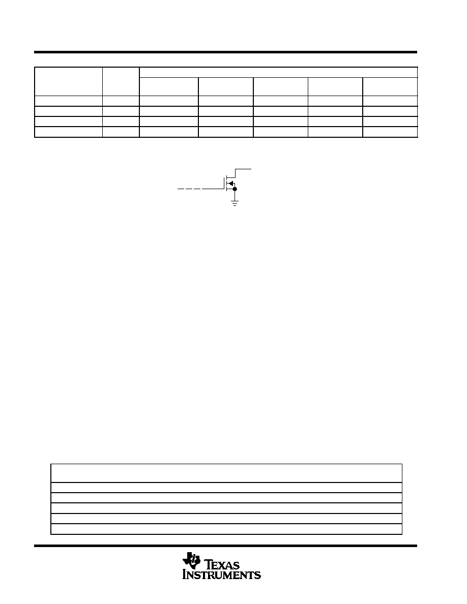
AVAILABLE OPTIONS
V
max
PACKAGES
TA
VIOmax
at 25
∞
C
SMALL OUTLINE
(D)
CHIP CARRIER
(FK)
CERAMIC DIP
(JG)
PLASTIC DIP
(P)
TSSOP
(PW)
0
∞
C to 70
∞
C
5 mV
TLC393CD
--
--
TLC393CP
TLC393CPWLE
- 40
∞
C to 85
∞
C
5 mV
TLC393ID
--
--
TLC393IP
TLC393IPWLE
- 40
∞
C to 125
∞
C
5 mV
TLC393QD
--
--
--
--
- 55
∞
C to 125
∞
C
5 mV
TLC393MD
TLC193MFK
TLC193MJG
TLC393MP
--
The D package is available taped and reeled. Add the suffix R to the device type (e.g., TLC393CDR).
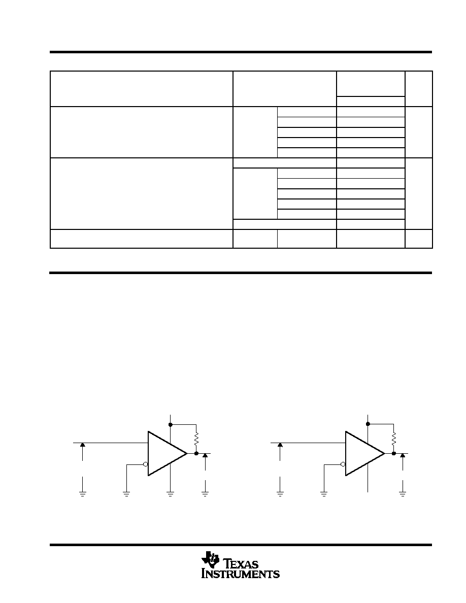
schematic
OUT
OPEN-DRAIN CMOS OUTPUT
absolute maximum ratings over operating free-air temperature range (unless otherwise noted)
Supply voltage range, V
DD
(see Note 1)
- 0.3 V to 18 V
. . . . . . . . . . . . . . . . . . . . . . . . . . . . . . . . . . . . . . . . . . . . .
Differential input voltage, V
ID
(see Note 2)
±
18 V
. . . . . . . . . . . . . . . . . . . . . . . . . . . . . . . . . . . . . . . . . . . . . . . . . . .
Input voltage range, V
I
- 0.3 V to V
DD
. . . . . . . . . . . . . . . . . . . . . . . . . . . . . . . . . . . . . . . . . . . . . . . . . . . . . . . . . . . . .
Output voltage range, V
O
- 0.3 V to 16 V
. . . . . . . . . . . . . . . . . . . . . . . . . . . . . . . . . . . . . . . . . . . . . . . . . . . . . . . . . .
Input current, I
I
±
5 mA
. . . . . . . . . . . . . . . . . . . . . . . . . . . . . . . . . . . . . . . . . . . . . . . . . . . . . . . . . . . . . . . . . . . . . . . . . .
Output current, I
O
(each output)
20 mA
. . . . . . . . . . . . . . . . . . . . . . . . . . . . . . . . . . . . . . . . . . . . . . . . . . . . . . . . . . .
Total supply current into V
DD
40
mA
. . . . . . . . . . . . . . . . . . . . . . . . . . . . . . . . . . . . . . . . . . . . . . . . . . . . . . . . . . . . . .
Total current out of GND
40 mA
. . . . . . . . . . . . . . . . . . . . . . . . . . . . . . . . . . . . . . . . . . . . . . . . . . . . . . . . . . . . . . . . . .
Continuous total power dissipation
See Dissipation Rating Table
. . . . . . . . . . . . . . . . . . . . . . . . . . . . . . . . . . . . .
Operating free-air temperature range: TLC393C
0
∞
C to 70
∞
C
. . . . . . . . . . . . . . . . . . . . . . . . . . . . . . . . . . . . . . .
TLC393I
- 40
∞
C to 85
∞
C
. . . . . . . . . . . . . . . . . . . . . . . . . . . . . . . . . . . . . .
TLC393Q
- 40
∞
C to 125
∞
C
. . . . . . . . . . . . . . . . . . . . . . . . . . . . . . . . . . .
TLC393M
- 55
∞
C to 125
∞
C
. . . . . . . . . . . . . . . . . . . . . . . . . . . . . . . . . . .
TLC193M
- 55
∞
C to 125
∞
C
. . . . . . . . . . . . . . . . . . . . . . . . . . . . . . . . . . .
Storage temperature range
- 65
∞
C to 150
∞
C
. . . . . . . . . . . . . . . . . . . . . . . . . . . . . . . . . . . . . . . . . . . . . . . . . . . . . . .
Case temperature for 60 seconds: FK package
260
∞
C
. . . . . . . . . . . . . . . . . . . . . . . . . . . . . . . . . . . . . . . . . . . . . .
Lead temperature 1,6 mm (1/16 inch) from case for 10 seconds: D or P package
260
∞
C
. . . . . . . . . . . . . . . . .
Lead temperature 1,6 mm (1/16 inch) from case for 60 seconds: JG package
300
∞
C
. . . . . . . . . . . . . . . . . . . .
Stresses beyond those listed under "absolute maximum ratings" may cause permanent damage to the device. These are stress ratings only, and
functional operation of the device at these or any other conditions beyond those indicated under "recommended operating conditions" is not
implied. Exposure to absolute-maximum-rated conditions for extended periods may affect device reliability.
NOTES:
1. All voltage values, except differential voltages, are with respect to network ground.
2. Differential voltages are at IN+ with respect to IN -.
DISSIPATION RATING TABLE
PACKAGE
TA
25
∞
C
POWER RATING
DERATING FACTOR
ABOVE TA = 25
∞
C
TA = 70
∞
C
POWER RATING
TA = 85
∞
C
POWER RATING
TA = 125
∞
C
POWER RATING
D
725 mW
5.8 mW/
∞
C
464 mW
377 mW
145 mW
FK
1375 mW
11.0 mW/
∞
C
880 mW
715 mW
275 mW
JG
1050 mW
8.4 mW/
∞
C
672 mW
546 mW
210 mW
P
1000 mW
8.0 mW/
∞
C
640 mW
520 mW
--
PW
525 mW
4.2 mW/
∞
C
336 mW
273 mW
--
TLC193, TLC393
DUAL MICROPOWER LinCMOS
VOLTAGE COMPARATOR
SLCS115E - DECEMBER 1986 - REVISED JULY 2003
3
POST OFFICE BOX 655303
∑
DALLAS, TEXAS 75265
POST OFFICE BOX 1443
∑
HOUSTON, TEXAS 77251-1443
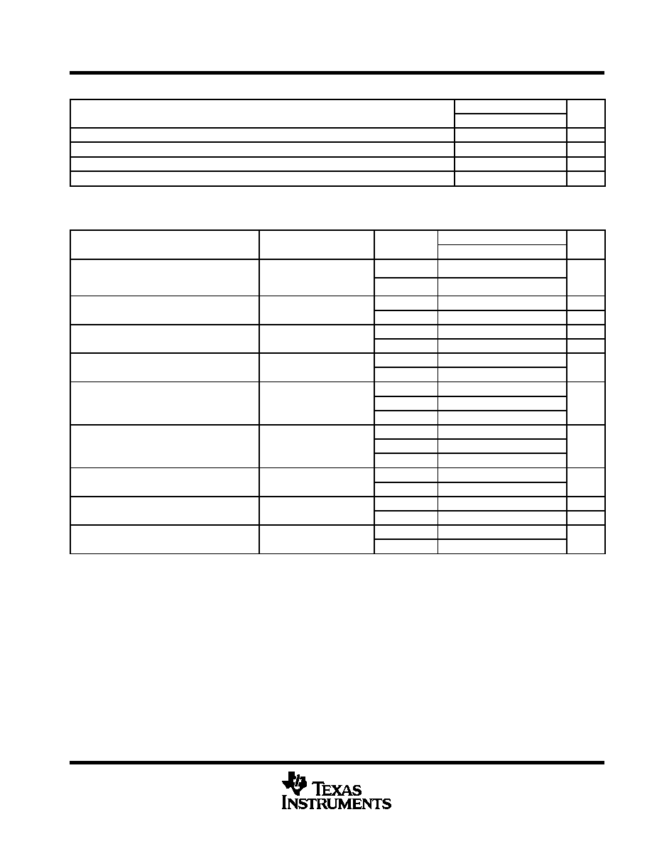
recommended operating conditions
TLC393C
UNIT
MIN
NOM
MAX
UNIT
Supply voltage, VDD
3
5
16
V
Common-mode input voltage, VIC
-0.2
VDD - 1.5
V
Low-level output current, IOL
20
mA
Operating free-air temperature, TA
0
70
∞
C
electrical characteristics at specified operating free-air temperature, V
DD
= 5 V (unless otherwise
noted)
PARAMETER
TEST CONDITIONS
T
TLC393C
UNIT
PARAMETER
TEST CONDITIONS
TA
MIN
TYP
MAX
UNIT
V
Inp t offset oltage
VIC = VICRmin,
VDD 5 V to 10 V
25
∞
C
1.4
5
mV
VIO
Input offset voltage
VDD = 5 V to 10 V,
See Note 3
0
∞
C to 70
∞
C
6.5
mV
I
Inp t offset c rrent
V
2 5 V
25
∞
C
1
pA
IIO
Input offset current
VIC = 2.5 V
70
∞
C
0.3
nA
I
Inp t bias c rrent
V
2 5 V
25
∞
C
5
pA
IIB
Input bias current
VIC = 2.5 V
70
∞
C
0.6
nA
V
Common mode inp t oltage range
25
∞
C
0 to VDD - 1
V
VICR
Common-mode input voltage range
0
∞
C to 70
∞
C
0 to VDD - 1.5
V
25
∞
C
84
CMMR
Common-mode rejection ratio
VIC = VICRmin
70
∞
C
84
dB
CMMR
Common mode rejection ratio
VIC VICRmin
0
∞
C
84
dB
25
∞
C
85
kSVR
Supply-voltage rejection ratio
VDD = 5 V to 10 V
70
∞
C
85
dB
kSVR
Su
ly voltage rejection ratio
VDD 5 V to 10 V
0
∞
C
85
dB
V
Lo
le el o tp t oltage
V
1 V
I
6 mA
25
∞
C
300
400
mV
VOL
Low-level output voltage
VID = -1 V, IOL = 6 mA
70
∞
C
650
mV
I
High le el o tp t c rrent
V
1 V
V
5 V
25
∞
C
0.8
40
nA
IOH
High-level output current
VID = 1 V,
VO = 5 V
70
∞
C
1
µ
A
IDD
Supply current (both comparators)
Outputs low No load
25
∞
C
22
40
µ
A
IDD
Supply current (both comparators)
Outputs low, No load
0
∞
C to 70
∞
C
50
µ
A
All characteristics are measured with zero common-mode voltage unless otherwise noted.
NOTE 3: The offset voltage limits given are the maximum values required to drive the output up to 4.5 V or down to 0.3 V.
TLC193, TLC393
DUAL MICROPOWER LinCMOS
VOLTAGE COMPARATOR
SLCS115D - DECEMBER 1986 - REVISED JULY 2003
4
POST OFFICE BOX 655303
∑
DALLAS, TEXAS 75265
POST OFFICE BOX 1443
∑
HOUSTON, TEXAS 77251-1443
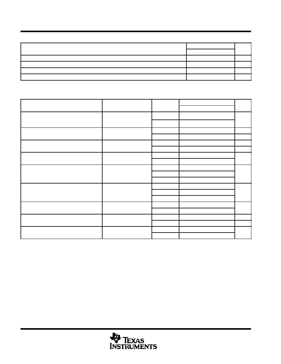
recommended operating conditions
TLC393I
UNIT
MIN
NOM
MAX
UNIT
Supply voltage, VDD
3
5
16
V
Common-mode input voltage, VIC
- 0.2
VDD - 1.5
V
Low-level output current, IOL
20
mA
Operating free-air temperature, TA
- 40
85
∞
C
electrical characteristics at specified operating free-air temperature, V
DD
= 5 V (unless otherwise
noted)
PARAMETER
TEST CONDITIONS
T
TLC393I
UNIT
PARAMETER
TEST CONDITIONS
TA
MIN
TYP
MAX
UNIT
V
Inp t offset oltage
VIC = VICRmin,
VDD 5 V to 10 V
25
∞
C
1.4
5
mV
VIO
Input offset voltage
VDD = 5 V to 10 V,
See Note 3
-40
∞
C to 85
∞
C
7
mV
I
Inp t offset c rrent
V
2 5 V
25
∞
C
1
pA
IIO
Input offset current
VIC = 2.5 V
85
∞
C
1
nA
I
Inp t bias c rrent
V
2 5 V
25
∞
C
5
pA
IIB
Input bias current
VIC = 2.5 V
85
∞
C
2
nA
V
Common mode inp t oltage range
25
∞
C
0 to VDD - 1
V
VICR
Common-mode input voltage range
-40
∞
C to 85
∞
C
0 to VDD - 1.5
V
25
∞
C
84
CMMR
Common-mode rejection ratio
VIC = VICRmin
85
∞
C
84
dB
CMMR
Common mode rejection ratio
VIC VICRmin
- 40
∞
C
84
dB
25
∞
C
85
kSVR
Supply-voltage rejection ratio
VDD = 5 V to 10 V
85
∞
C
85
dB
kSVR
Su
ly voltage rejection ratio
VDD 5 V to 10 V
- 40
∞
C
84
dB
V
Lo
le el o tp t oltage
V
1 V
I
6 mA
25
∞
C
300
400
mV
VOL
Low-level output voltage
VID = -1 V, IOL = 6 mA
85
∞
C
700
mV
I
High le el o tp t c rrent
V
1 V
V
5 V
25
∞
C
0.8
40
nA
IOH
High-level output current
VID = 1 V,
VO = 5 V
85
∞
C
1
µ
A
IDD
Supply current (both comparators)
Outputs low No load
25
∞
C
22
40
µ
A
IDD
Supply current (both comparators)
Outputs low, No load
-40
∞
C to 85
∞
C
65
µ
A
All characteristics are measured with zero common-mode voltage unless otherwise noted.
NOTE 3: The offset voltage limits given are the maximum values required to drive the output up to 4.5 V or down to 0.3 V.

TLC193, TLC393
DUAL MICROPOWER LinCMOS
VOLTAGE COMPARATOR
SLCS115E - DECEMBER 1986 - REVISED JULY 2003
5
POST OFFICE BOX 655303
∑
DALLAS, TEXAS 75265
POST OFFICE BOX 1443
∑
HOUSTON, TEXAS 77251-1443
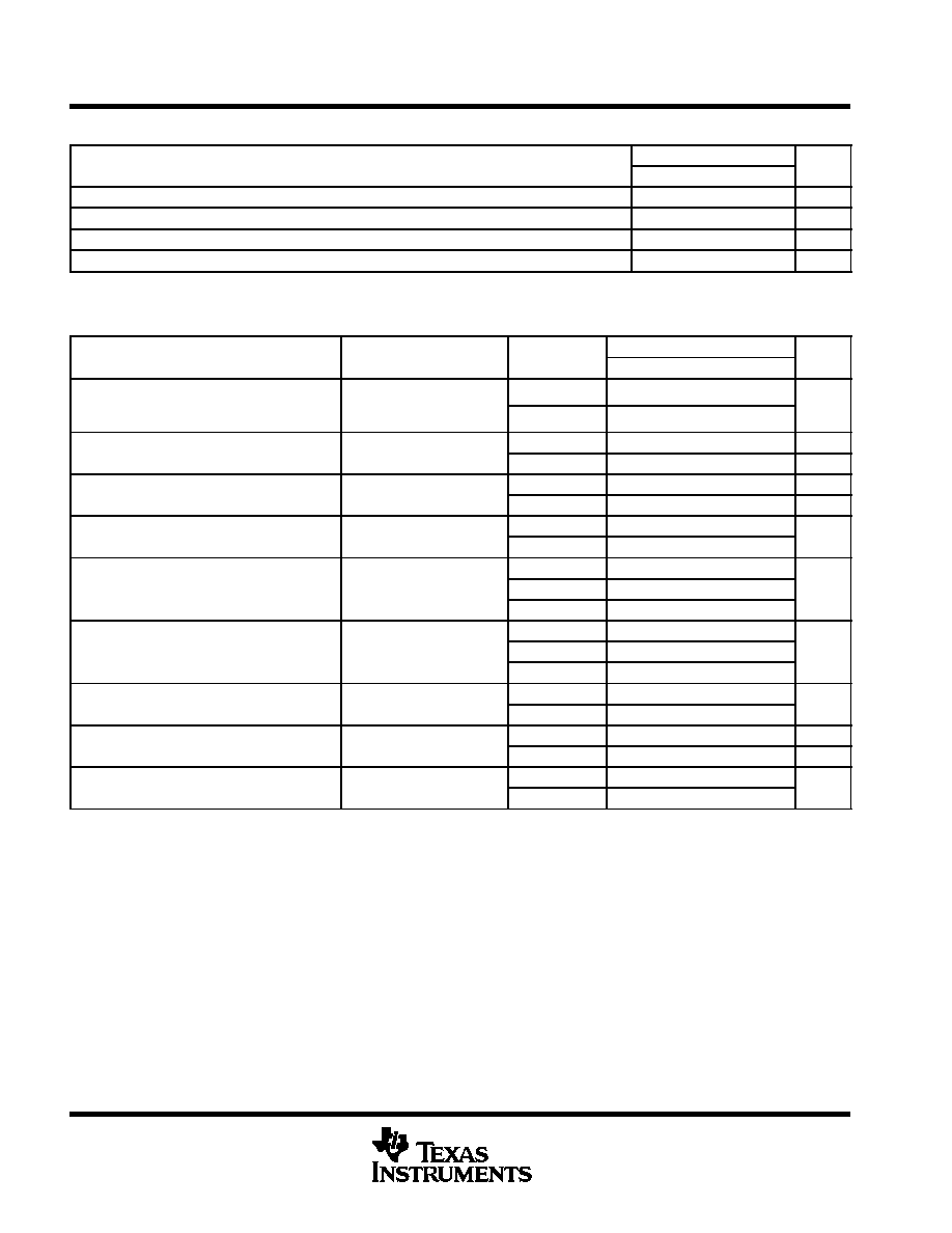
recommended operating conditions
TLC393Q
UNIT
MIN
NOM
MAX
UNIT
Supply voltage, VDD
4
5
16
V
Common-mode input voltage, VIC
0
VDD - 1.5
V
Low-level output current, IOL
20
mA
Operating free-air temperature, TA
-40
125
∞
C
electrical characteristics at specified operating free-air temperature, V
DD
= 5 V (unless otherwise
noted)
PARAMETER
TEST CONDITIONS
T
TLC393Q
UNIT
PARAMETER
TEST CONDITIONS
TA
MIN
TYP
MAX
UNIT
V
Inp t offset oltage
VIC = VICRmin,
VDD 5 V to 10 V
25
∞
C
1.4
5
mV
VIO
Input offset voltage
VDD = 5 V to 10 V,
See Note 4
-40
∞
C to 125
∞
C
10
mV
I
Inp t offset c rrent
V
2 5 V
25
∞
C
1
pA
IIO
Input offset current
VIC = 2.5 V
125
∞
C
15
nA
I
Inp t bias c rrent
V
2 5 V
25
∞
C
5
pA
IIB
Input bias current
VIC = 2.5 V
125
∞
C
30
nA
V
Common mode inp t oltage range
25
∞
C
0 to VDD - 1
V
VICR
Common-mode input voltage range
-40
∞
C to 125
∞
C
0 to VDD - 1.5
V
25
∞
C
84
CMMR
Common-mode rejection ratio
VIC = VICRmin
125
∞
C
84
dB
CMMR
Common mode rejection ratio
VIC VICRmin
-40
∞
C
84
dB
25
∞
C
85
kSVR
Supply-voltage rejection ratio
VDD = 5 V to 10 V
125
∞
C
84
dB
kSVR
Su
ly voltage rejection ratio
VDD 5 V to 10 V
-40
∞
C
84
dB
V
Lo
le el o tp t oltage
V
1 V
I
6 mA
25
∞
C
300
400
mV
VOL
Low-level output voltage
VID = -1 V, IOL = 6 mA
125
∞
C
800
mV
I
High le el o tp t c rrent
V
1 V
V
5 V
25
∞
C
0.8
40
nA
IOH
High-level output current
VID = 1 V,
VO = 5 V
125
∞
C
1
µ
A
IDD
Supply current (both comparators)
Outputs low No load
25
∞
C
22
40
µ
A
IDD
Supply current (both comparators)
Outputs low, No load
-40
∞
C to 125
∞
C
90
µ
A
All characteristics are measured with zero common-mode voltage unless otherwise noted.
NOTE 4: The offset voltage limits given are the maximum values required to drive the output up to 4.5 V or down to 0.3 V (with a 2.5-k
load to
VDD).
TLC193, TLC393
DUAL MICROPOWER LinCMOS
VOLTAGE COMPARATOR
SLCS115D - DECEMBER 1986 - REVISED JULY 2003
6
POST OFFICE BOX 655303
∑
DALLAS, TEXAS 75265
POST OFFICE BOX 1443
∑
HOUSTON, TEXAS 77251-1443
recommended operating conditions
TLC193M, TLC393M
UNIT
MIN
NOM
MAX
UNIT
Supply voltage, VDD
4
5
16
V
Common-mode input voltage, VIC
0
VDD - 1.5
V
Low-level output current, IOL
20
mA
Operating free-air temperature, TA
-55
125
∞
C
electrical characteristics at specified operating free-air temperature, V
DD
= 5 V (unless otherwise
noted)
PARAMETER
TEST CONDITIONS
T
TLC193M, TLC393M
UNIT
PARAMETER
TEST CONDITIONS
TA
MIN
TYP
MAX
UNIT
V
Inp t offset oltage
VIC = VICRmin,
VDD 5 V to 10 V
25
∞
C
1.4
5
mV
VIO
Input offset voltage
VDD = 5 V to 10 V,
See Note 4
-55
∞
C to 125
∞
C
10
mV
I
Inp t offset c rrent
V
2 5 V
25
∞
C
1
pA
IIO
Input offset current
VIC = 2.5 V
125
∞
C
15
nA
I
Inp t bias c rrent
V
2 5 V
25
∞
C
5
pA
IIB
Input bias current
VIC = 2.5 V
125
∞
C
30
nA
V
Common mode inp t oltage range
25
∞
C
0 to VDD - 1
V
VICR
Common-mode input voltage range
-55
∞
C to 125
∞
C
0 to VDD - 1.5
V
25
∞
C
84
CMMR
Common-mode rejection ratio
VIC = VICRmin
125
∞
C
84
dB
CMMR
Common mode rejection ratio
VIC VICRmin
-55
∞
C
84
dB
25
∞
C
85
kSVR
Supply-voltage rejection ratio
VDD = 5 V to 10 V
125
∞
C
84
dB
kSVR
Su
ly voltage rejection ratio
VDD 5 V to 10 V
-55
∞
C
84
dB
V
Lo
le el o tp t oltage
V
1 V
I
6 mA
25
∞
C
300
400
mV
VOL
Low-level output voltage
VID = -1 V, IOL = 6 mA
125
∞
C
800
mV
I
High le el o tp t c rrent
V
1 V
V
5 V
25
∞
C
0.8
40
nA
IOH
High-level output current
VID = 1 V,
VO = 5 V
125
∞
C
1
µ
A
IDD
Supply current (both comparators)
Outputs low No load
25
∞
C
22
40
µ
A
IDD
Supply current (both comparators)
Outputs low, No load
-55
∞
C to 125
∞
C
90
µ
A
All characteristics are measured with zero common-mode voltage unless otherwise noted.
NOTE 4: The offset voltage limits given are the maximum values required to drive the output up to 4.5 V or down to 0.3 V (with a 2.5-k
load to
VDD).
TLC193, TLC393
DUAL MICROPOWER LinCMOS
VOLTAGE COMPARATOR
SLCS115E - DECEMBER 1986 - REVISED JULY 2003
7
POST OFFICE BOX 655303
∑
DALLAS, TEXAS 75265
POST OFFICE BOX 1443
∑
HOUSTON, TEXAS 77251-1443
switching characteristics, V
DD
= 5 V, T
A
= 25
∞
C (see Figure 3)
PARAMETER
TEST CONDITIONS
TLC393C, TLC393I
TLC393Q, TLC193M,
TLC393M
UNIT
MIN
TYP
MAX
Overdrive = 2 mV
4.5
f
10 kH
Overdrive = 5 mV
2.5
tPLH
Propagation delay time, low-to-high-level output
f = 10 kHz,
CL = 15 pF
Overdrive = 10 mV
1.7
µ
s
tPLH
Pro agation delay time, low to high level out ut
CL = 15 pF
Overdrive = 20 mV
1.2
µ
s
Overdrive = 40 mV
1.1
VI = 1.4-V step at IN +
1.1
Overdrive = 2 mV
3.6
f
10 kH
Overdrive = 5 mV
2.1
tPHL
Propagation delay time, high-to-low-level output
f = 10 kHz,
CL = 15 pF
Overdrive = 10 mV
1.3
µ
s
tPHL
Pro agation delay time, high to low level out ut
CL = 15 pF
Overdrive = 20 mV
0.85
µ
s
Overdrive = 40 mV
0.55
VI = 1.4-V step at IN +
0.10
tf
Fall time, output
f = 10 kHz,
CL = 15 pF
Overdrive = 50 mV
22
ns
PARAMETER MEASUREMENT INFORMATION
The TLC393 contains a digital output stage which, if held in the linear region of the transfer curve, can cause
damage to the device. Conventional operational amplifier/comparator testing incorporates the use of a servo
loop that is designed to force the device output to a level within this linear region. Since the servo-loop method
of testing cannot be used, the following alternatives for testing parameters such as input offset voltage,
common-mode rejection ratio, etc., are suggested.
To verify that the input offset voltage falls within the limits specified, the limit value is applied to the input as shown
in Figure 1(a). With the noninverting input positive with respect to the inverting input, the output should be high.
With the input polarity reversed, the output should be low.
A similar test can be made to verify the input offset voltage at the common-mode extremes. The supply voltages
can be slewed as shown in Figure 1(b) for the V
ICR
test, rather than changing the input voltages, to provide
greater accuracy.
+
-
5 V
Applied VIO
Limit
VO
+
-
1 V
Applied VIO
Limit
VO
- 4 V
(a) VIO WITH VIC = 0 V
(b) VIO WITH VIC = 4 V
5.1 k
5.1 k
Figure 1. Method for Verifying That Input Offset Voltage Is Within Specified Limits
TLC193, TLC393
DUAL MICROPOWER LinCMOS
VOLTAGE COMPARATOR
SLCS115D - DECEMBER 1986 - REVISED JULY 2003
8
POST OFFICE BOX 655303
∑
DALLAS, TEXAS 75265
POST OFFICE BOX 1443
∑
HOUSTON, TEXAS 77251-1443
PARAMETER MEASUREMENT INFORMATION
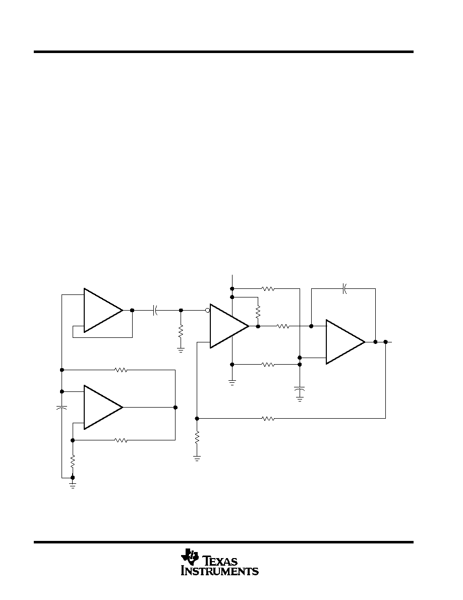
A close approximation of the input offset voltage can be obtained by using a binary search method to vary the
differential input voltage while monitoring the output state. When the applied input voltage differential is equal,
but opposite in polarity, to the input offset voltage, the output changes states.
Figure 2 illustrates a practical circuit for direct dc measurement of input offset voltage that does not bias the
comparator in the linear region. The circuit consists of a switching-mode servo loop in which U1A generates
a triangular waveform of approximately 20-mV amplitude. U1B acts as a buffer, with C2 and R4 removing any
residual dc offset. The signal is then applied to the inverting input of the comparator under test, while the
noninverting input is driven by the output of the integrator formed by U1C through the voltage divider formed
by R9 and R10. The loop reaches a stable operating point when the output of the comparator under test has
a duty cycle of exactly 50%, which can only occur when the incoming triangle wave is sliced symmetrically or
when the voltage at the noninverting input exactly equals the input offset voltage.
The voltage divider formed by R9 and R10 provides an increase in input offset voltage by a factor of 100 to
make measurement easier. The values of R5, R8, R9, and R10 can significantly influence the accuracy of the
reading; therefore, it is suggested that their tolerance level be 1% or lower.
Measuring the extremely low values of input current requires isolation from all other sources of leakage current
and compensation for the leakage of the test socket and board. With a good picoammeter, the socket and board
leakage can be measured with no device in the socket. Subsequently, this open-socket leakage value can be
subtracted from the measurement obtained with a device in the socket to obtain the actual input current of the
device.
-
+
DUT
VDD
+
-
-
+
-
+
C2
1
µ
F
R4
47 k
R5
1.8 k
,
1%
C3
0.68
µ
F
U1C
1/4 TLC274CN
U1B
1/4 TLC274CN
U1A
1/4 TLC274CN
R7
1 M
R8
1.8 k
,
1%
R9
10 k
,
1%
R1
240 k
R2
10 k
C1
0.1
µ
F
R3
100 k
C4
0.1
µ
F
Integrator
R10
100
,
1%
Buffer
Triangle
Generator
VIO
(X100)
R6
5.1 k
Figure 2. Circuit for Input Offset Voltage Measurement

TLC193, TLC393
DUAL MICROPOWER LinCMOS
VOLTAGE COMPARATOR
SLCS115E - DECEMBER 1986 - REVISED JULY 2003
9
POST OFFICE BOX 655303
∑
DALLAS, TEXAS 75265
POST OFFICE BOX 1443
∑
HOUSTON, TEXAS 77251-1443
PARAMETER MEASUREMENT INFORMATION
Propagation delay time is defined as the interval between the application of an input step function and the instant
when the output reaches 50% of its maximum value. Propagation delay time, low-to-high-level output, is
measured from the leading edge of the input pulse, while propagation delay time, high-to-low-level output, is
measured from the trailing edge of the input pulse. Propagation delay time measurement at low input signal
levels can be greatly affected by the input offset voltage. The offset voltage should be balanced by the
adjustment at the inverting input (as shown in Figure 3) so that the circuit is just at the transition point. Then a
low signal, for example, 105 mV or 5 mV overdrive, causes the output to change state.
DUT
VDD
CL
(see Note A)
Pulse
Generator
10
10 Turn
1 V
- 1 V
1 k
50
1
µ
F
0.1
µ
F
TEST CIRCUIT
100 mV
Input
Overdrive
50%
tPLH
100 mV
Input
Overdrive
90%
50%
10%
tf
tPHL
Low-to-High-
Level Output
High-to-Low-
Level Output
VOLTAGE WAVEFORMS
5.1 k
Input Offset Voltage
Compensation
Adjustment
90%
tr
10%
NOTE A: CL includes probe and jig capacitance.
Figure 3. Propagation Delay, Rise Time, and Fall Time Circuit and Voltage Waveforms

TLC193, TLC393
DUAL MICROPOWER LinCMOS
VOLTAGE COMPARATOR
SLCS115D - DECEMBER 1986 - REVISED JULY 2003
10
POST OFFICE BOX 655303
∑
DALLAS, TEXAS 75265
POST OFFICE BOX 1443
∑
HOUSTON, TEXAS 77251-1443
TYPICAL CHARACTERISTICS
Table of Graphs
FIGURE
VIO
Input offset voltage
Distribution
4
IIB
Input bias current
vs Free-air temperature
5
CMRR
Common-mode rejection ratio
vs Free-air temperature
6
kSVR
Supply-voltage rejection ratio
vs Free-air temperature
7
V
Lo
le el o tp t oltage
vs Low-level output current
8
VOL
Low-level output voltage
vs Low level out ut current
vs Free-air temperature
8
9
I
Lo
le el o tp t c rrent
vs High-level output voltage
10
IOH
Low-level output current
vs High level out ut voltage
vs Free-air temperature
10
11
I
S ppl c rrent
vs Supply voltage
12
IDD
Supply current
vs Su
ly voltage
vs Free-air temperature
12
13
tPLH
Low-to-high level output propagation delay time
vs Supply voltage
14
tPHL
High-to-low level output propagation delay time
vs Supply voltage
15
Low-to-high-level output response
Low-to-high level output propagation delay time
16
High-to-low level output response
High-to-low level output propagation delay time
17
tf
Fall time
vs Supply voltage
18
Figure 4
……
……
……
«
«
«
«
«
«
«
«
«
…
…
…
…
…
…
…
…
…
…
««
««
««
««
««
««
««
««
««
««
««
««
««
««
««
««
««
««
««
««
««
…
…
…
…
…
…
…
…
…
«
«
«
«
……
………
«
«
«
«
«
«
«
«
«
……
……
……
……
……
…
…
…
…
…
…
…
«
Number of Units
VDD = 5 V
VIC = 2.5 V
TA = 25
∞
C
- 5
- 4
- 3
- 2
- 1
0
1
2
3
4
5
VIO - Input Offset Voltage - mV
DISTRIBUTION OF INPUT
OFFSET VOLTAGE
100
90
80
70
60
50
40
30
20
10
0
«
……
……
……
……
……
……
Figure 5
I
TA - Free-Air Temperature -
∞
C
IB
-
Input Bias Current
-
nA
25
50
75
100
125
10
1
0.1
0.01
0.001
INPUT BIAS CURRENT
vs
FREE-AIR TEMPERATURE
VDD = 5 V
VIC = 2.5 V
Data at high and low temperatures are applicable only within the rated operating free-air temperature ranges of the various devices.
TLC193, TLC393
DUAL MICROPOWER LinCMOS
VOLTAGE COMPARATOR
SLCS115E - DECEMBER 1986 - REVISED JULY 2003
11
POST OFFICE BOX 655303
∑
DALLAS, TEXAS 75265
POST OFFICE BOX 1443
∑
HOUSTON, TEXAS 77251-1443
TYPICAL CHARACTERISTICS
Figure 6
CMRR
-
Common-Mode
TA - Free-Air Temperature -
∞
C
COMMON-MODE REJECTION RATIO
vs
FREE-AIR TEMPERATURE
Rejection Ratio
-
dB
- 75
- 50
- 25
0
25
50
75
100
125
90
89
88
87
86
85
84
83
82
81
80
VDD = 5 V
Figure 7
-
Supply V
oltage Rejection Ratio
-
dB
TA - Free-Air Temperature -
∞
C
SUPPLY VOLTAGE REJECTION RATIO
vs
FREE-AIR TEMPERATURE
- 75
- 50
- 25
0
25
50
75
100
125
90
89
88
87
86
85
84
83
82
81
80
VDD = 5 V to 10 V
SVR
k
Figure 8
IOL - Low-Level Output Current - mA
0
2
4
6
8
10
12
14
16
18
20
V
OL
-
Low-Level Output V
o
ltage
-
V
LOW-LEVEL OUTPUT VOLTAGE
vs
LOW-LEVEL OUTPUT CURRENT
4 V
10 V
VDD = 16 V
5 V
1.5
1.25
1
0.75
0.5
0.25
0
TA = 25
∞
C
VDD = 3 V
Figure 9
- 75
- 50
- 25
0
25
50
75
100
125
TA - Free-Air Temperature -
∞
C
LOW-LEVEL OUTPUT VOLTAGE
vs
FREE-AIR TEMPERATURE
V
OL
-
Low-Level Output V
oltage
-
mV
600
500
400
300
200
100
0
VDD = 5 V
IOL = 6 mA
Data at high and low temperatures are applicable only within the rated operating free-air temperature ranges of the various devices.
TLC193, TLC393
DUAL MICROPOWER LinCMOS
VOLTAGE COMPARATOR
SLCS115D - DECEMBER 1986 - REVISED JULY 2003
12
POST OFFICE BOX 655303
∑
DALLAS, TEXAS 75265
POST OFFICE BOX 1443
∑
HOUSTON, TEXAS 77251-1443
TYPICAL CHARACTERISTICS
Figure 10
I OH
-
High-Level Output Current
-
nA
0
2
4
6
8
10
12
14
16
VOH - High-Level Output Voltage - V
HIGH-LEVEL OUTPUT CURRENT
vs
HIGH-LEVEL OUTPUT VOLTAGE
1000
100
10
1
0.1
TA = 25
∞
C
TA = 125
∞
C
TA = 85
∞
C
TA = 70
∞
C
VOH = VDD
Figure 11
TA - Free-Air Temperature -
∞
C
I OH
-
High-Level Output Current
-
nA
25
50
75
100
125
HIGH-LEVEL OUTPUT CURRENT
vs
FREE-AIR TEMPERATURE
1000
100
10
1
0.1
VDD = VOH = 5 V
Figure 12
SUPPLY CURRENT
vs
SUPPLY VOLTAGE
VDD - Supply Voltage - V
40
35
30
25
20
15
10
5
0
0
2
4
6
8
10
12
14
16
I
-
Supply Current
-
µ
DD
A
TA = - 55
∞
C
TA = 125
∞
C
TA = 85
∞
C
TA = - 40
∞
C
Outputs Low
No Loads
TA = 25
∞
C
50
45
Figure 13
SUPPLY CURRENT
vs
FREE-AIR TEMPERATURE
30
25
20
15
10
5
0
- 75
- 50
- 25
0
25
50
75
100
125
TA - Free-Air Temperature -
∞
C
I DD
-
Supply Current
-
µ
A
40
35
Outputs High
Outputs Low
VDD = 5 V
No Load
Data at high and low temperatures are applicable only within the rated operating free-air temperature ranges of the various devices.

TLC193, TLC393
DUAL MICROPOWER LinCMOS
VOLTAGE COMPARATOR
SLCS115E - DECEMBER 1986 - REVISED JULY 2003
13
POST OFFICE BOX 655303
∑
DALLAS, TEXAS 75265
POST OFFICE BOX 1443
∑
HOUSTON, TEXAS 77251-1443
TYPICAL CHARACTERISTICS
Figure 14
LOW-TO-HIGH-LEVEL
OUTPUT RESPONSE TIME
vs
SUPPLY VOLTAGE
Overdrive = 2 mV
5 mV
10 mV
40 mV
6
5
4
3
2
1
0
0
2
4
6
8
10
12
14
16
VDD - Supply Voltage - V
CL = 15 pF
RL = 5.1 k
(pullup to VDD)
TA = 25
∞
C
t
PLH
-
Low-to-High-Level
20 mV
Output Propagation Delay T
ime
-
µ
s
Figure 15
HIGH-TO-LOW-LEVEL
OUTPUT RESPONSE TIME
vs
SUPPLY VOLTAGE
3
2.5
2
1.5
1
0.5
0
0
2
4
6
8
10
12
14
16
VDD - Supply Voltage - V
t
PHL
-
High-to-Low Level
Output Propagation Delay T
ime
-
µ
s
Overdrive = 2 mV
CL = 15 pF
RL = 5.1 k
(pullup to VDD)
TA = 25
∞
C
5
4.5
4
3.5
5 mV
10 mV
20 mV
40 mV
Figure 16
0
1
2
3
4
5
V
O
-
Output
V
o
ltage
-
V
V
oltage
-
mV
Differential Input
LOW-TO-HIGH-LEVEL OUTPUT
PROPAGATION DELAY
FOR VARIOUS INPUT OVERDRIVES
tPLH - Low-to-High-Level Output
Propagation Delay Time -
µ
s
VDD = 5 V
CL = 15 pF
RL = 5.1 k
(pullup to VDD)
TA = 25
∞
C
5
0
100
0
40 mV
20 mV
10 mV
5 mV
2 mV
Figure 17
40 mV
20 mV
10 mV
5 mV
2 mV
HIGH-TO-LOW-LEVEL OUTPUT
PROPAGATION DELAY
FOR VARIOUS INPUT OVERDRIVES
tPHL - High-to-Low-Level Output
Propagation Delay Time -
µ
s
V
O
-
Output
V
o
ltage
-
V
V
oltage
-
mV
Differential Input
5
0
100
0
0
1
2
3
4
5
VDD = 5 V
CL = 15 pF
RL = 5.1 k
(pullup to VDD)
TA = 25
∞
C
TLC193, TLC393
DUAL MICROPOWER LinCMOS
VOLTAGE COMPARATOR
SLCS115D - DECEMBER 1986 - REVISED JULY 2003
14
POST OFFICE BOX 655303
∑
DALLAS, TEXAS 75265
POST OFFICE BOX 1443
∑
HOUSTON, TEXAS 77251-1443
TYPICAL CHARACTERISTICS
0
2
4
6
8
10
VDD - Supply Voltage - V
t
f
-
Fall T
ime
-
ns
OUTPUT FALL TIME
vs
SUPPLY VOLTAGE
60
50
40
30
20
0
10
50-mV Overdrive
RL = 5.1 k
(pullup to VDD)
TA = 25
∞
C
12
14
16
CL = 100 pF
15 pF
50 pF
Figure 18
APPLICATION INFORMATION
The input should always remain within the supply rails in order to avoid forward biasing the diodes in the electrostatic
discharge (ESD) protection structure. If either input exceeds this range, the device will not be damaged as long as
the input current is limited to less than 5 mA. To maintain the expected output state, the inputs must remain within
the common-mode range. For example, at 25
∞
C with V
DD
= 5 V, both inputs must remain between -0.2 V and 4 V
to assure proper device operation.
To assure reliable operation, the supply should be decoupled with a capacitor (0.1-
µ
F) positioned as close to the
device as possible.
The TLC393 has internal ESD-protection circuits that prevent functional failures at voltages up to 2000 V as tested
under MIL-STD-883C, Method 3015.2; however, care should be exercised in handling these devices, as exposure
to ESD may result in the degradation of the device parametric performance.
Table of Applications
FIGURE
Pulse-width-modulated motor speed controller
19
Enhanced supply supervisor
20
Two-phase nonoverlapping clock generator
21
Micropower switching regulator
28

TLC193, TLC393
DUAL MICROPOWER LinCMOS
VOLTAGE COMPARATOR
SLCS115E - DECEMBER 1986 - REVISED JULY 2003
15
POST OFFICE BOX 655303
∑
DALLAS, TEXAS 75265
POST OFFICE BOX 1443
∑
HOUSTON, TEXAS 77251-1443
APPLICATION INFORMATION
C1
0.01
µ
F
(see Note B)
5 V
1/2 TLC393
Motor Speed Control
Potentiometer
+
-
+
-
10 k
100 k
10 k
10 k
1/2 TLC393
10 k
5 V
DIR
EN
SN75603
Half-H Driver
12 V
Motor
DIR
EN
12 V
Direction
Control
S1
SPDT
5 V
5 V
C2
(see Note A)
5.1 k
5.1 k
12 V
SN75604
Half-H Driver
NOTES: A. The recommended minimum capacitance is 10
µ
F to eliminate common ground switching noise.
B. Adjust C1 for change in oscillator frequency.
Figure 19. Pulse-Width-Modulated Motor Speed Controller

TLC193, TLC393
DUAL MICROPOWER LinCMOS
VOLTAGE COMPARATOR
SLCS115D - DECEMBER 1986 - REVISED JULY 2003
16
POST OFFICE BOX 655303
∑
DALLAS, TEXAS 75265
POST OFFICE BOX 1443
∑
HOUSTON, TEXAS 77251-1443
APPLICATION INFORMATION
1/2 TLC393
To
µ
P Interrupt
Early Power Fail
+
-
+
-
1 k
3.3 k
CT
(see Note B)
1/2 TLC393
10 k
5 V
5 V
12-V
Sense
R2
R1
VUNREG
(see Note A)
1
µ
F
12 V
RESIN
REF
CT
GND
RESET
SENSE
VCC
To
µ
P
Reset
Monitors 5-VDC Rail
Monitors 12-VDC Rail
Early Power Fail Warning
TL7705A
2.5 V
5.1 k
5.1 k
12 V
NOTES: A.
V
UNREG
+
2.5
(R1 +R2)
R2
B. The value of CT determines the time delay of reset.
Figure 20. Enhanced Supply Supervisor
TLC193, TLC393
DUAL MICROPOWER LinCMOS
VOLTAGE COMPARATOR
SLCS115E - DECEMBER 1986 - REVISED JULY 2003
17
POST OFFICE BOX 655303
∑
DALLAS, TEXAS 75265
POST OFFICE BOX 1443
∑
HOUSTON, TEXAS 77251-1443
APPLICATION INFORMATION
-
+
22 k
C1
0.01
µ
F
(see Note A)
1/2 TLC393
R1
100
(see Note B)
100 k
1/2 TLC393
2OUT
-
+
-
+
1/2 TLC393
100 k
100 k
12 V
1OUT
12 V
R2
5 k
(see Note C)
R3
100 k
(see Note B)
2OUT
1OUT
12 V
5.1 k
12 V
5.1 k
12 V
5.1 k
NOTES: A. Adjust C1 for a change in oscillator frequency where:
1/f = 1.85(100 k
)C1
B. Adjust R1 and R3 to change duty cycle
C. Adjust R2 to change deadtime
Figure 21. Two-Phase Nonoverlapping Clock Generator
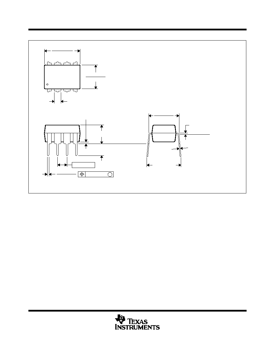
MECHANICAL DATA
MCER001A ≠ JANUARY 1995 ≠ REVISED JANUARY 1997
1
POST OFFICE BOX 655303
∑
DALLAS, TEXAS 75265
JG (R-GDIP-T8)
CERAMIC DUAL-IN-LINE
0.310 (7,87)
0.290 (7,37)
0.014 (0,36)
0.008 (0,20)
Seating Plane
4040107/C 08/96
5
4
0.065 (1,65)
0.045 (1,14)
8
1
0.020 (0,51) MIN
0.400 (10,16)
0.355 (9,00)
0.015 (0,38)
0.023 (0,58)
0.063 (1,60)
0.015 (0,38)
0.200 (5,08) MAX
0.130 (3,30) MIN
0.245 (6,22)
0.280 (7,11)
0.100 (2,54)
0
∞
≠15
∞
NOTES: A. All linear dimensions are in inches (millimeters).
B. This drawing is subject to change without notice.
C. This package can be hermetically sealed with a ceramic lid using glass frit.
D. Index point is provided on cap for terminal identification.
E. Falls within MIL STD 1835 GDIP1-T8
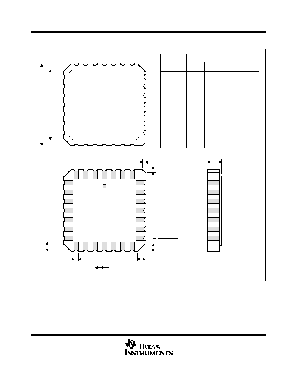
MECHANICAL DATA
MLCC006B ≠ OCTOBER 1996
1
POST OFFICE BOX 655303
∑
DALLAS, TEXAS 75265
FK (S-CQCC-N**)
LEADLESS CERAMIC CHIP CARRIER
4040140 / D 10/96
28 TERMINAL SHOWN
B
0.358
(9,09)
MAX
(11,63)
0.560
(14,22)
0.560
0.458
0.858
(21,8)
1.063
(27,0)
(14,22)
A
NO. OF
MIN
MAX
0.358
0.660
0.761
0.458
0.342
(8,69)
MIN
(11,23)
(16,26)
0.640
0.739
0.442
(9,09)
(11,63)
(16,76)
0.962
1.165
(23,83)
0.938
(28,99)
1.141
(24,43)
(29,59)
(19,32)
(18,78)
**
20
28
52
44
68
84
0.020 (0,51)
TERMINALS
0.080 (2,03)
0.064 (1,63)
(7,80)
0.307
(10,31)
0.406
(12,58)
0.495
(12,58)
0.495
(21,6)
0.850
(26,6)
1.047
0.045 (1,14)
0.045 (1,14)
0.035 (0,89)
0.035 (0,89)
0.010 (0,25)
12
13
14
15
16
18
17
11
10
8
9
7
5
4
3
2
0.020 (0,51)
0.010 (0,25)
6
1
28
26
27
19
21
B SQ
A SQ
22
23
24
25
20
0.055 (1,40)
0.045 (1,14)
0.028 (0,71)
0.022 (0,54)
0.050 (1,27)
NOTES: A. All linear dimensions are in inches (millimeters).
B. This drawing is subject to change without notice.
C. This package can be hermetically sealed with a metal lid.
D. The terminals are gold plated.
E. Falls within JEDEC MS-004
MECHANICAL DATA
MPDI001A ≠ JANUARY 1995 ≠ REVISED JUNE 1999
1
POST OFFICE BOX 655303
∑
DALLAS, TEXAS 75265
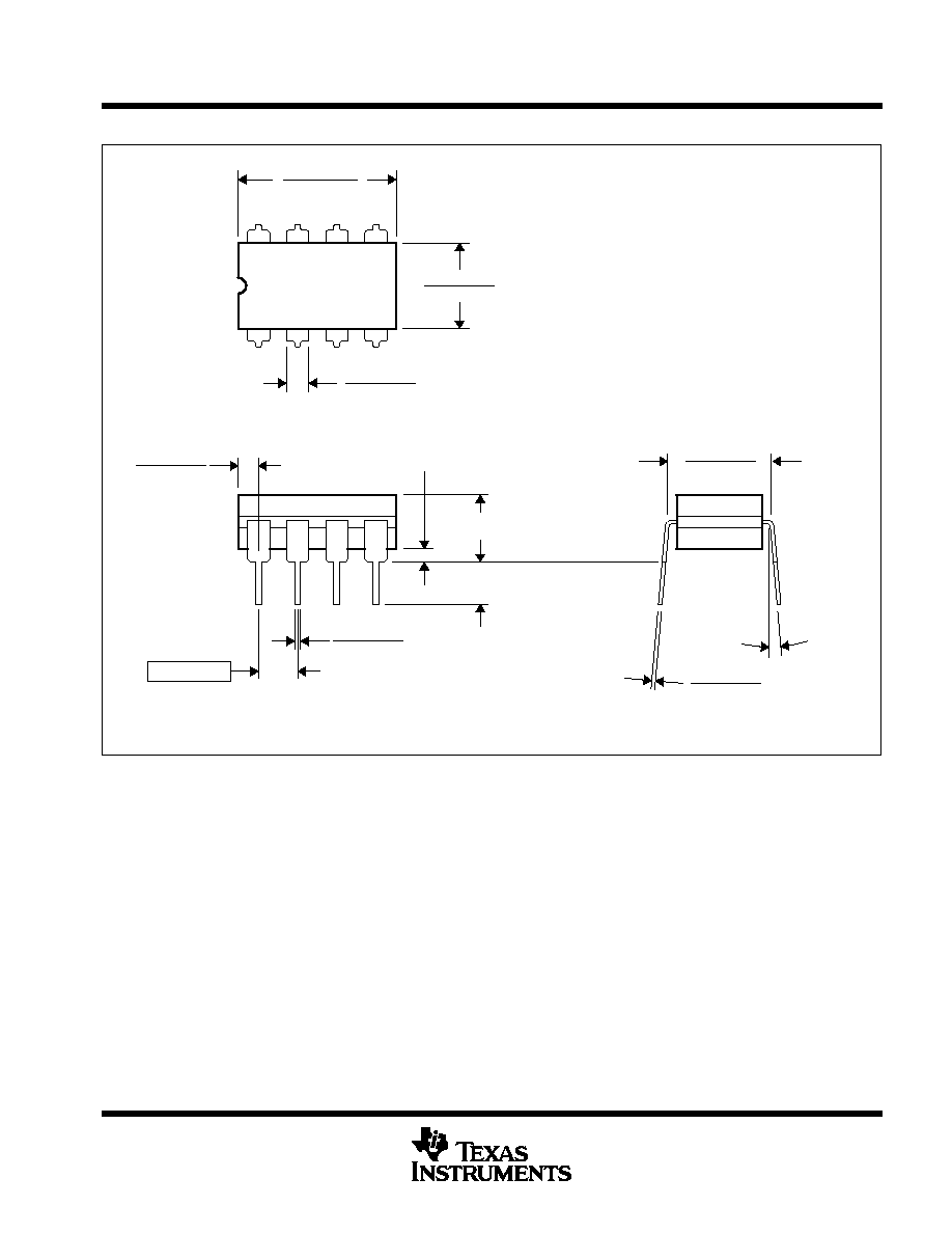
P (R-PDIP-T8)
PLASTIC DUAL-IN-LINE
8
4
0.015 (0,38)
Gage Plane
0.325 (8,26)
0.300 (7,62)
0.010 (0,25) NOM
MAX
0.430 (10,92)
4040082/D 05/98
0.200 (5,08) MAX
0.125 (3,18) MIN
5
0.355 (9,02)
0.020 (0,51) MIN
0.070 (1,78) MAX
0.240 (6,10)
0.260 (6,60)
0.400 (10,60)
1
0.015 (0,38)
0.021 (0,53)
Seating Plane
M
0.010 (0,25)
0.100 (2,54)
NOTES: A. All linear dimensions are in inches (millimeters).
B. This drawing is subject to change without notice.
C. Falls within JEDEC MS-001
For the latest package information, go to http://www.ti.com/sc/docs/package/pkg_info.htm

MECHANICAL DATA
MSOI002B ≠ JANUARY 1995 ≠ REVISED SEPTEMBER 2001
1
POST OFFICE BOX 655303
∑
DALLAS, TEXAS 75265
D (R-PDSO-G**)
PLASTIC SMALL-OUTLINE PACKAGE
8 PINS SHOWN
8
0.197
(5,00)
A MAX
A MIN
(4,80)
0.189
0.337
(8,55)
(8,75)
0.344
14
0.386
(9,80)
(10,00)
0.394
16
DIM
PINS **
4040047/E 09/01
0.069 (1,75) MAX
Seating Plane
0.004 (0,10)
0.010 (0,25)
0.010 (0,25)
0.016 (0,40)
0.044 (1,12)
0.244 (6,20)
0.228 (5,80)
0.020 (0,51)
0.014 (0,35)
1
4
8
5
0.150 (3,81)
0.157 (4,00)
0.008 (0,20) NOM
0
∞
≠ 8
∞
Gage Plane
A
0.004 (0,10)
0.010 (0,25)
0.050 (1,27)
NOTES: A. All linear dimensions are in inches (millimeters).
B. This drawing is subject to change without notice.
C. Body dimensions do not include mold flash or protrusion, not to exceed 0.006 (0,15).
D. Falls within JEDEC MS-012


MECHANICAL DATA
MTSS001C ≠ JANUARY 1995 ≠ REVISED FEBRUARY 1999
1
POST OFFICE BOX 655303
∑
DALLAS, TEXAS 75265
PW (R-PDSO-G**)
PLASTIC SMALL-OUTLINE PACKAGE
14 PINS SHOWN
0,65
M
0,10
0,10
0,25
0,50
0,75
0,15 NOM
Gage Plane
28
9,80
9,60
24
7,90
7,70
20
16
6,60
6,40
4040064/F 01/97
0,30
6,60
6,20
8
0,19
4,30
4,50
7
0,15
14
A
1
1,20 MAX
14
5,10
4,90
8
3,10
2,90
A MAX
A MIN
DIM
PINS **
0,05
4,90
5,10
Seating Plane
0
∞
≠ 8
∞
NOTES: A. All linear dimensions are in millimeters.
B. This drawing is subject to change without notice.
C. Body dimensions do not include mold flash or protrusion not to exceed 0,15.
D. Falls within JEDEC MO-153

IMPORTANT NOTICE
Texas Instruments Incorporated and its subsidiaries (TI) reserve the right to make corrections, modifications,
enhancements, improvements, and other changes to its products and services at any time and to discontinue
any product or service without notice. Customers should obtain the latest relevant information before placing
orders and should verify that such information is current and complete. All products are sold subject to TI's terms
and conditions of sale supplied at the time of order acknowledgment.
TI warrants performance of its hardware products to the specifications applicable at the time of sale in
accordance with TI's standard warranty. Testing and other quality control techniques are used to the extent TI
deems necessary to support this warranty. Except where mandated by government requirements, testing of all
parameters of each product is not necessarily performed.
TI assumes no liability for applications assistance or customer product design. Customers are responsible for
their products and applications using TI components. To minimize the risks associated with customer products
and applications, customers should provide adequate design and operating safeguards.
TI does not warrant or represent that any license, either express or implied, is granted under any TI patent right,
copyright, mask work right, or other TI intellectual property right relating to any combination, machine, or process
in which TI products or services are used. Information published by TI regarding third-party products or services
does not constitute a license from TI to use such products or services or a warranty or endorsement thereof.
Use of such information may require a license from a third party under the patents or other intellectual property
of the third party, or a license from TI under the patents or other intellectual property of TI.
Reproduction of information in TI data books or data sheets is permissible only if reproduction is without
alteration and is accompanied by all associated warranties, conditions, limitations, and notices. Reproduction
of this information with alteration is an unfair and deceptive business practice. TI is not responsible or liable for
such altered documentation.
Resale of TI products or services with statements different from or beyond the parameters stated by TI for that
product or service voids all express and any implied warranties for the associated TI product or service and
is an unfair and deceptive business practice. TI is not responsible or liable for any such statements.
Following are URLs where you can obtain information on other Texas Instruments products and application
solutions:
Products
Applications
Amplifiers
amplifier.ti.com
Audio
www.ti.com/audio
Data Converters
dataconverter.ti.com
Automotive
www.ti.com/automotive
DSP
dsp.ti.com
Broadband
www.ti.com/broadband
Interface
interface.ti.com
Digital Control
www.ti.com/digitalcontrol
Logic
logic.ti.com
Military
www.ti.com/military
Power Mgmt
power.ti.com
Optical Networking
www.ti.com/opticalnetwork
Microcontrollers
microcontroller.ti.com
Security
www.ti.com/security
Telephony
www.ti.com/telephony
Video & Imaging
www.ti.com/video
Wireless
www.ti.com/wireless
Mailing Address:
Texas Instruments
Post Office Box 655303 Dallas, Texas 75265
Copyright
2003, Texas Instruments Incorporated