
SN54ABT2245, SN74ABT2245
OCTAL TRANSCEIVERS AND LINE/MOS DRIVERS
WITH 3-STATE OUTPUTS
SCBS234D ≠ SEPTEMBER 1992 ≠ REVISED MAY 1997
1
POST OFFICE BOX 655303
∑
DALLAS, TEXAS 75265
D
B-Port Outputs Have Equivalent 25-
Series Resistors, So No External Resistors
Are Required
D
State-of-the-Art
EPIC-
B
TM
BiCMOS Design
Significantly Reduces Power Dissipation
D
Latch-Up Performance Exceeds 500 mA Per
JEDEC Standard JESD-17
D
ESD Protection Exceeds 2000 V Per
MIL-STD-833, Method 3015; Exceeds 200 V
Using Machine Model (C = 200 pF, R = 0)
D
Typical V
OLP
(Output Ground Bounce) < 1 V
at V
CC
= 5 V, T
A
= 25
∞
C
D
High-Impedance State During Power Up
and Power Down
D
Package Options Include Plastic
Small-Outline (DW), Shrink Small-Outline
(DB), and Thin Shrink Small-Outline (PW)
Packages, Ceramic Chip Carriers (FK),
Plastic (N) and Ceramic (J) DIPs, and
Ceramic Flat (W) Package
description
These octal transceivers and line drivers are
designed for asynchronous communication
between data buses. The devices transmit data
from the A bus to the B bus or from the B bus to
the A bus, depending on the logic level at the
direction-control (DIR) input. The output-enable
(OE) input can be used to disable the device so
the buses are effectively isolated.
The B-port outputs, which are designed to sink up to 12 mA, include equivalent 25-
series resistors to reduce
overshoot and undershoot.
When V
CC
is between 0 and 2.1 V, the device is in the high-impedance state during power up or power down.
However, to ensure the high-impedance state above 2.1 V, OE should be tied to V
CC
through a pullup resistor;
the minimum value of the resistor is determined by the current-sinking/current-sourcing capability of the driver.
The SN54ABT2245 is characterized for operation over the full military temperature range of ≠55
∞
C to 125
∞
C.
The SN74ABT2245 is characterized for operation from ≠40
∞
C to 85
∞
C.
FUNCTION TABLE
INPUTS
OPERATION
OE
DIR
OPERATION
L
L
B data to A bus
L
H
A data to B bus
H
X
Isolation
Copyright
©
1997, Texas Instruments Incorporated
PRODUCTION DATA information is current as of publication date.
Products conform to specifications per the terms of Texas Instruments
standard warranty. Production processing does not necessarily include
testing of all parameters.
EPIC-
B is a trademark of Texas Instruments Incorporated.
Please be aware that an important notice concerning availability, standard warranty, and use in critical applications of
Texas Instruments semiconductor products and disclaimers thereto appears at the end of this data sheet.
SN54ABT2245 . . . J OR W PACKAGE
SN74ABT2245 . . . DB, DW, N, OR PW PACKAGE
(TOP VIEW)
3 2
1 20 19
9 10 11 12 13
4
5
6
7
8
18
17
16
15
14
B1
B2
B3
B4
B5
A3
A4
A5
A6
A7
A2
A1
DIR
B7
B6
OE
A8
GND
B8
V
CC
SN54ABT2245 . . . FK PACKAGE
(TOP VIEW)
1
2
3
4
5
6
7
8
9
10
20
19
18
17
16
15
14
13
12
11
DIR
A1
A2
A3
A4
A5
A6
A7
A8
GND
V
CC
OE
B1
B2
B3
B4
B5
B6
B7
B8

SN54ABT2245, SN74ABT2245
OCTAL TRANSCEIVERS AND LINE/MOS DRIVERS
WITH 3-STATE OUTPUTS
SCBS234D ≠ SEPTEMBER 1992 ≠ REVISED MAY 1997
2
POST OFFICE BOX 655303
∑
DALLAS, TEXAS 75265
logic symbol
This symbol is in accordance with ANSI/IEEE Std 91-1984 and IEC Publication 617-12.
B2
17
B3
16
B4
15
A5
6
A6
7
A7
8
A8
9
A2
3
A3
4
A4
5
OE
A1
2
G3
19
3 EN2 [AB]
B5
14
B6
13
B7
12
B8
11
B1
18
3 EN1 [BA]
1
DIR
1
2
logic diagram (positive logic)
DIR
OE
A1
B1
To Seven Other Channels
1
2
19
18
SN54ABT2245, SN74ABT2245
OCTAL TRANSCEIVERS AND LINE/MOS DRIVERS
WITH 3-STATE OUTPUTS
SCBS234D ≠ SEPTEMBER 1992 ≠ REVISED MAY 1997
3
POST OFFICE BOX 655303
∑
DALLAS, TEXAS 75265
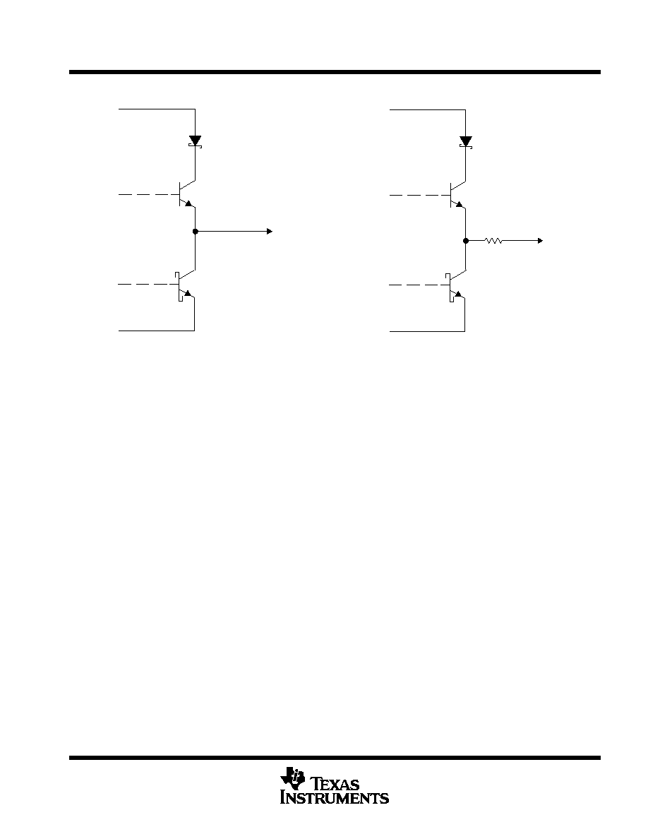
schematic of A-port outputs
Output
VCC
GND
All resistor values shown are nominal.
schematic of B-port outputs
Output
VCC
GND
25
absolute maximum ratings over operating free-air temperature range (unless otherwise noted)
Supply voltage range, V
CC
≠0.5 V to 7 V
. . . . . . . . . . . . . . . . . . . . . . . . . . . . . . . . . . . . . . . . . . . . . . . . . . . . . . . . . .
Input voltage range, V
I
(except I/O ports) (see Note 1)
≠0.5 V to 7 V
. . . . . . . . . . . . . . . . . . . . . . . . . . . . . . . . . .
Voltage range applied to any output in the high or power-off state, V
O
≠0.5 V to 5.5 V
. . . . . . . . . . . . . . . . . . .
Current into any output in the low state, I
O
: SN54ABT2245 (except B port)
96 mA
. . . . . . . . . . . . . . . . . . . . . .
SN74ABT2245 (except B port)
128 mA
. . . . . . . . . . . . . . . . . . . . .
B port
30 mA
. . . . . . . . . . . . . . . . . . . . . . . . . . . . . . . . . . . . . . . . . . . .
Input clamp current, I
IK
(V
I
< 0)
≠18 mA
. . . . . . . . . . . . . . . . . . . . . . . . . . . . . . . . . . . . . . . . . . . . . . . . . . . . . . . . . . .
Output clamp current, I
OK
(V
O
< 0)
≠50 mA
. . . . . . . . . . . . . . . . . . . . . . . . . . . . . . . . . . . . . . . . . . . . . . . . . . . . . . . .
Package thermal impedance,
JA
(see Note 2): DB package
115
∞
C/W
. . . . . . . . . . . . . . . . . . . . . . . . . . . . . . . . .
DW package
97
∞
C/W
. . . . . . . . . . . . . . . . . . . . . . . . . . . . . . . . .
N package
67
∞
C/W
. . . . . . . . . . . . . . . . . . . . . . . . . . . . . . . . . . .
PW package
128
∞
C/W
. . . . . . . . . . . . . . . . . . . . . . . . . . . . . . . .
Storage temperature range, T
stg
≠65
∞
C to 150
∞
C
. . . . . . . . . . . . . . . . . . . . . . . . . . . . . . . . . . . . . . . . . . . . . . . . . . .
Stresses beyond those listed under "absolute maximum ratings" may cause permanent damage to the device. These are stress ratings only, and
functional operation of the device at these or any other conditions beyond those indicated under "recommended operating conditions" is not
implied. Exposure to absolute-maximum-rated conditions for extended periods may affect device reliability.
NOTES:
1. The input and output negative-voltage ratings may be exceeded if the input and output clamp-current ratings are observed.
2. The package thermal impedance is calculated in accordance with EIA/JEDEC Std JESD51, except for through-hole packages,
which use a trace length of zero.
SN54ABT2245, SN74ABT2245
OCTAL TRANSCEIVERS AND LINE/MOS DRIVERS
WITH 3-STATE OUTPUTS
SCBS234D ≠ SEPTEMBER 1992 ≠ REVISED MAY 1997
4
POST OFFICE BOX 655303
∑
DALLAS, TEXAS 75265
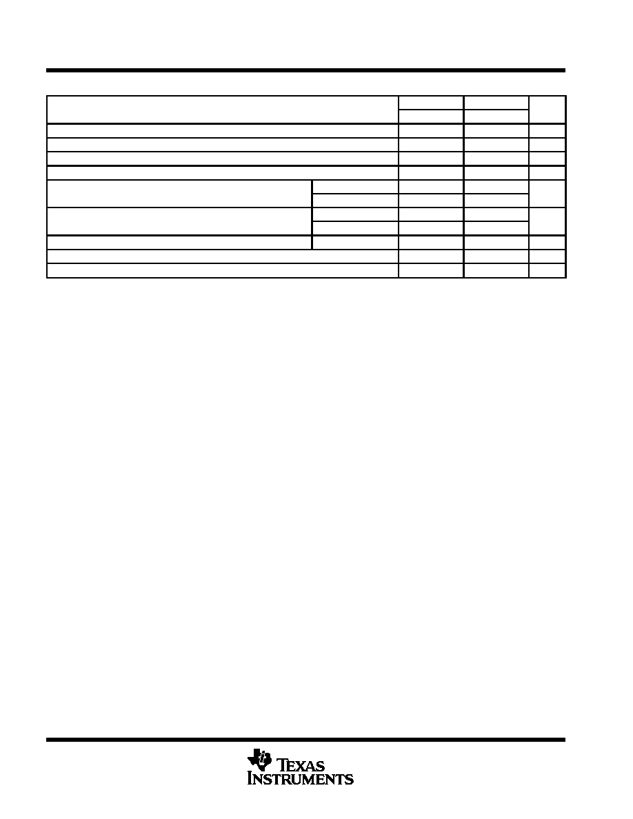
recommended operating conditions (see Note 3)
SN54ABT2245
SN74ABT2245
UNIT
MIN
MAX
MIN
MAX
UNIT
VCC
Supply voltage
4.5
5.5
4.5
5.5
V
VIH
High-level input voltage
2
2
V
VIL
Low-level input voltage
0.8
0.8
V
VI
Input voltage
0
VCC
0
VCC
V
IOH
High level output current
A port
≠24
≠32
mA
IOH
High-level output current
B port
≠12
≠12
mA
IOL
Low level output current
A port
48
64
mA
IOL
Low-level output current
B port
12
12
mA
t/
v
Input transition rise or fall rate
Outputs enabled
5
5
ns/V
t/
VCC
Power-up ramp rate
200
200
µ
s/V
TA
Operating free-air temperature
≠55
125
≠40
85
∞
C
NOTE 3: Unused pins (input or I/O) must be held high or low to prevent them from floating.
SN54ABT2245, SN74ABT2245
OCTAL TRANSCEIVERS AND LINE/MOS DRIVERS
WITH 3-STATE OUTPUTS
SCBS234D ≠ SEPTEMBER 1992 ≠ REVISED MAY 1997
5
POST OFFICE BOX 655303
∑
DALLAS, TEXAS 75265
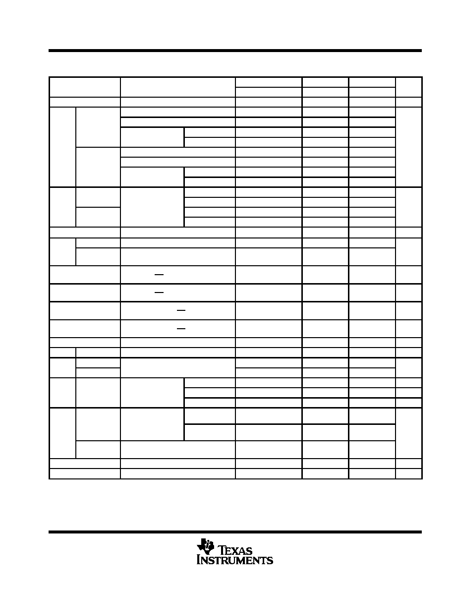
electrical characteristics over recommended operating free-air temperature range (unless
otherwise noted)
PARAMETER
TEST CONDITIONS
TA = 25
∞
C
SN54ABT2245
SN74ABT2245
UNIT
PARAMETER
TEST CONDITIONS
MIN
TYP
MAX
MIN
MAX
MIN
MAX
UNIT
VIK
VCC = 4.5 V,
II = ≠18 mA
≠1.2
≠1.2
≠1.2
V
VCC = 4.5 V,
IOH = ≠1 mA
3.35
3.3
3.35
B port
VCC = 5 V,
IOH = ≠1 mA
3.85
3.8
3.85
B port
VCC = 4 5 V
IOH = ≠3 mA
3
3.1
VOH
VCC = 4.5 V
IOH = ≠12 mA
2.6
2.6
V
VOH
VCC = 4.5 V,
IOH = ≠3 mA
2.5
2.5
2.5
V
A port
VCC = 5 V,
IOH = ≠3 mA
3
3
3
A port
VCC = 4 5 V
IOH = ≠24 mA
2
2
VCC = 4.5 V
IOH = ≠32 mA
2*
2
B port
IOL = 8 mA
0.65
0.8
0.65
VOL
B port
VCC = 4 5 V
IOL = 12 mA
0.8
0.8
V
VOL
A port
VCC = 4.5 V
IOL = 48 mA
0.55
0.55
V
A port
IOL = 64 mA
0.55*
0.55
Vhys
100
mV
Control inputs
VCC = 0 to 5.5 V, VI = VCC or GND
±
1
±
1
±
1
II
A or B ports
VCC = 2.1 V to 5.5 V,
VI = VCC or GND
±
20
±
20
±
20
µ
A
IOZH
VCC = 2.1 V to 5.5 V,
VO = 2.7 V, OE
2 V
10
10
10
µ
A
IOZL
VCC = 2.1 V to 5.5 V,
VO = 0.5 V, OE
2 V
≠10
≠10
≠10
µ
A
IOZPUß
VCC = 0 to 2.1 V,
VO = 0.5 V to 2.7 V, OE = X
±
50
±
50
±
50
µ
A
IOZPDß
VCC = 2.1 V to 0,
VO = 0.5 V to 2.7 V, OE = X
±
50
±
50
±
50
µ
A
Ioff
VCC = 0,
VI or VO
4.5 V
±
100
±
100
µ
A
ICEX
Outputs high
VCC = 5.5 V,
VO = 5.5 V
50
50
50
µ
A
I ∂
B port
VCC = 5 5 V
VO = 2 5 V
≠25
≠100
≠25
≠100
≠25
≠100
mA
IO∂
A port
VCC = 5.5 V,
VO = 2.5 V
≠50
≠100
≠180
≠50
≠180
≠50
≠180
mA
VCC = 5.5 V,
Outputs high
1
250
250
250
µ
A
ICC
A or B ports
VCC = 5.5 V,
IO = 0,
Outputs low
24
32
32
32
mA
VI = VCC or GND
Outputs disabled
0.5
250
250
250
µ
A
Data inputs
VCC = 5.5 V,
One input at 3.4 V,
Outputs enabled
1.5
1.5
1.5
ICC#
Data inputs
,
Other inputs at
VCC or GND
Outputs disabled
0.05
0.05
0.05
mA
Control inputs
VCC = 5.5 V, One input at 3.4 V,
Other inputs at VCC or GND
1.5
1.5
1.5
Ci
VI = 2.5 V or 0.5 V
3
pF
Cio
VO = 2.5 V or 0.5 V
6
pF
* On products compliant to MIL-PRF-38535, this parameter does not apply.
All typical values are at VCC = 5 V.
The parameters IOZH and IOZL include the input leakage current.
ß This parameter is characterized but not production tested.
∂ Not more than one output should be tested at a time, and the duration of the test should not exceed one second.
# This is the increase in supply current for each input that is at the specified TTL voltage level rather than VCC or GND.