
SN54ABT3614
64
◊
36
◊
2 CLOCKED BIDIRECTIONAL FIRST-IN, FIRST-OUT MEMORY
WITH BUS MATCHING AND BYTE SWAPPING
SGBS308F ≠ AUGUST 1995 ≠ REVISED MAY 2000
1
POST OFFICE BOX 655303
∑
DALLAS, TEXAS 75265
D
Free-Running CLKA and CLKB Can Be
Asynchronous or Coincident
D
Two Independent 64
◊
36 Clocked FIFOs
Buffering Data in Opposite Directions
D
Mailbox-Bypass Register for Each FIFO
D
Dynamic Port-B Bus Sizing of 36 Bits (Long
Word), 18 Bits (Word), and 9 Bits (Byte)
D
Selection of Big- or Little-Endian Format for
Word and Byte Bus Sizes
D
Three Modes of Byte-Order Swapping on
Port B
D
Almost-Full and Almost-Empty Flags
D
Microprocessor Interface Control Logic
D
EFA, FFA, AEA, and AFA Flags
Synchronized by CLKA
D
EFB, FFB, AEB, and AFB Flags
Synchronized by CLKB
D
Passive Parity Checking on Each Port
D
Parity Generation Can Be Selected for Each
Port
D
Low-Power Advanced BiCMOS Technology
D
Supports Clock Frequencies up to 50 MHz
D
Fast Access Times of 12 ns
D
Released as DSCC SMD (Standard
Microcircuit Drawing) 5962-9560901QYA
and 5962-9560901NXD
D
Package Options Include 132-Pin Ceramic
Quad Flat (HFP) and 120-Pin Plastic Quad
Flat (PCB) Packages
description
The SN54ABT3614 is a high-speed, low-power BiCMOS bidirectional clocked FIFO memory. It supports clock
frequencies up to 50 MHz and has read-access times as fast as 12 ns. Two independent 64
◊
36 dual-port SRAM
FIFOs in this device buffer data in opposite directions. Each FIFO has flags to indicate empty and full conditions
and two programmable flags (almost full and almost empty) to indicate when a selected number of words is
stored in memory. FIFO data on port B can be input and output in 36-bit, 18-bit, and 9-bit formats, with a choice
of big- or little-endian configurations. Three modes of byte-order swapping are possible with any bus-size
selection. Communication between each port can bypass the FIFOs via two 36-bit mailbox registers. Each
mailbox register has a flag to signal when new mail has been stored. Parity is checked passively on each port
and can be ignored if not desired. Parity generation can be selected for data read from each port.
The SN54ABT3614 is a clocked FIFO, which means each port employs a synchronous interface. All data
transfers through a port are gated to the low-to-high transition of a continuous (free-running) port clock by enable
signals. The continuous clocks for each port are independent of one another and can be asynchronous or
coincident. The enables for each port are arranged to provide a simple bidirectional interface between
microprocessors and/or buses controlled by a synchronous interface.
The full flag and almost-full flag of a FIFO are two-stage synchronized to the port clock that writes data to its
array. The empty flag and almost-empty flag of a FIFO are two-stage synchronized to the port clock that reads
data from its array.
The SN54ABT3614 is characterized for operation over the full military temperature range of ≠55
∞
C to 125
∞
C.
Copyright
©
2000, Texas Instruments Incorporated
PRODUCTION DATA information is current as of publication date.
Products conform to specifications per the terms of Texas Instruments
standard warranty. Production processing does not necessarily include
testing of all parameters.
Please be aware that an important notice concerning availability, standard warranty, and use in critical applications of
Texas Instruments semiconductor products and disclaimers thereto appears at the end of this data sheet.
On products compliant to MIL-PRF-38535, all parameters are tested
unless otherwise noted. On all other products, production
processing does not necessarily include testing of all parameters.
SN54ABT3614
64
◊
36
◊
2 CLOCKED BIDIRECTIONAL FIRST-IN, FIRST-OUT MEMORY
WITH BUS MATCHING AND BYTE SWAPPING
SGBS308F ≠ AUGUST 1995 ≠ REVISED MAY 2000
2
POST OFFICE BOX 655303
∑
DALLAS, TEXAS 75265
GND
AEA
EFA
A0
A1
A2
GND
A3
A4
A5
A6
V
CC
A7
A8
A9
GND
A10
A11
V
CC
A12
A13
A14
GND
A15
A16
A17
A18
A19
A20
GND
A21
A22
A23
GND
AEB
EFB
B0
B1
B2
GND
B3
B4
B5
B6
V
CC
B7
B8
B9
GND
B10
B11
V
CC
B12
B13
B14
GND
B15
B16
B17
B18
B19
B20
GND
B21
B22
B23
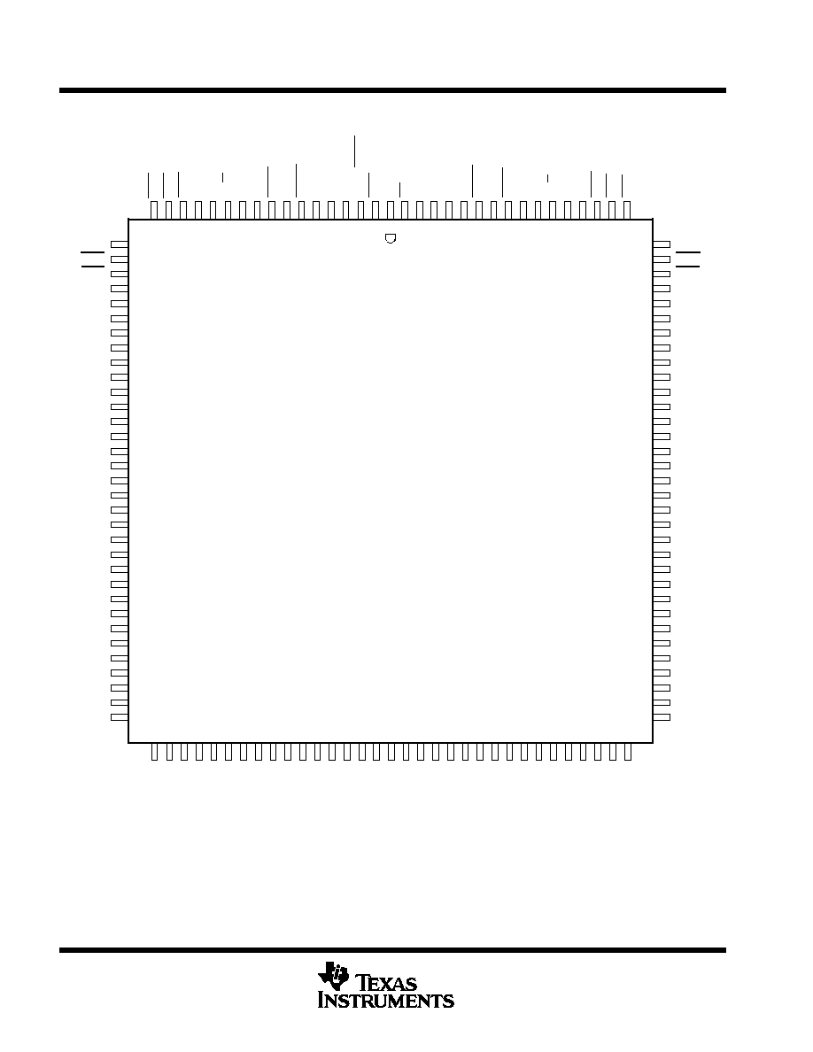
HFP PACKAGE
(TOP VIEW)
AF
A
FF
A
ENA
CLKA
W/RA
PGA
PEF
A
GND
MBF2
MBA
FS0
ODD/EVEN
RST
GND
BE
SW1
SW0
SIZ1
SIZ0
MBF1
GND
PGB
W/RB
CLKB
ENB
CSB
FFB
AFB
A24
A25
A26
GND
A27
CC
A29
A30
A31
A32
GND
A33
A34
A35
GND
B35
B34
GND
B32
B31
B30
B29
B28
B27
GND
B26
B25
B24
V
V
CC
CSA
V
CC
V
CC
FS1
PEFB
V
CC
V
CC
A28
B33
NC ≠ No internal connection
18
19
20
21
22
23
24
25
26
27
28
29
30
31
32
33
34
35
36
37
38
39
40
41
42
43
44
45
46
47
48
49
50
116
115
114
113
112
111
110
109
108
107
106
105
104
103
102
101
100
99
98
97
96
95
94
93
92
91
90
89
88
87
86
85
84
51 52 53 54 55 56 57 58 59 60 61 62 63 64 65 66 67 68 69 70 71 72 73 74 75 76 77 78 79 80 81 82 83
17 16 15 14 13 12 11 10 9 8 7 6 5 4 3 2 1 132
131
130
129
128
127
126
125
124
123
122
121
120
119
118
117
SN54ABT3614
64
◊
36
◊
2 CLOCKED BIDIRECTIONAL FIRST-IN, FIRST-OUT MEMORY
WITH BUS MATCHING AND BYTE SWAPPING
SGBS308F ≠ AUGUST 1995 ≠ REVISED MAY 2000
3
POST OFFICE BOX 655303
∑
DALLAS, TEXAS 75265
93
94
95
96
97
98
99
100
101
102
103
104
105
106
107
108
109
11
0
111
11
2
11
3
11
4
11
5
11
6
11
7
11
8
11
9
120
59
58
57
56
55
54
53
52
51
50
49
48
47
46
45
44
43
42
41
40
39
38
37
36
35
34
33
32
31
91
92
60
A24
A25
A26
A27
A28
GND
A30
A31
A32
A34
A35
GND
B35
B34
B33
B32
B31
B30
GND
B29
B28
B27
B26
B25
B24
B23
AF
A
FF
A
CSA
CLKA
W/RA
PEF
A
MBF2
MBA
FS1
FS0
ODD/EVEN
RST
GND
SW1
SW0
SIZ0
MBF1
PEFB
PGB
W/RB
CLKB
ENB
CSB
CC
V
CC
V
CC
V
BE
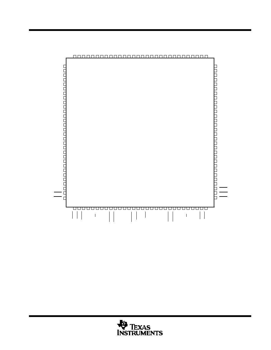
PCB PACKAGE
(TOP VIEW)
A33
CC
V
FFB
SIZ1
PGA
B22
B21
GND
B20
B19
B18
B17
B16
B15
B14
B13
B12
B11
B10
GND
B9
B8
B7
V
CC
B6
B5
B4
B3
GND
B2
B1
B0
EFB
AEB
AFB
A23
A22
A21
GND
A20
A19
A18
A17
A16
A15
A14
A13
A12
A11
A10
GND
A9
A8
A7
V
CC
A6
A5
A4
A3
GND
A2
A1
A0
EFA
AEA
A29
ENA
1
2
3
4
5
6
7
8
9
10
11
12
13
14
15
16
17
18
19
20
21
22
23
24
25
26
27
28
29
30
90
89
88
87
86
85
84
83
82
81
80
79
78
77
76
75
74
73
72
71
70
69
68
67
66
65
64
63
62
61
SN54ABT3614
64
◊
36
◊
2 CLOCKED BIDIRECTIONAL FIRST-IN, FIRST-OUT MEMORY
WITH BUS MATCHING AND BYTE SWAPPING
SGBS308F ≠ AUGUST 1995 ≠ REVISED MAY 2000
4
POST OFFICE BOX 655303
∑
DALLAS, TEXAS 75265
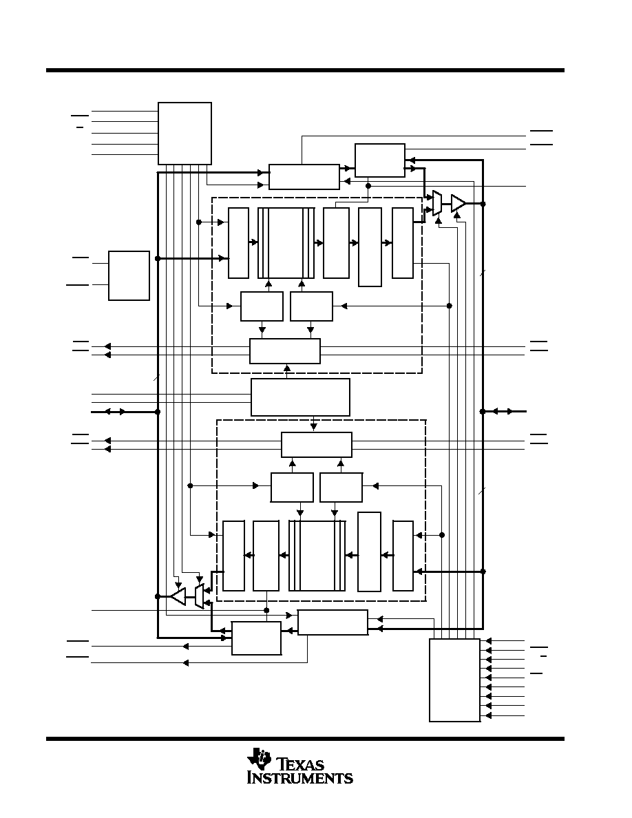
functional block diagram
Port-A
Control
Logic
AFA
FIFO1
Programmable-Flag
Offset Register
Read
Pointer
64
◊
36
SRAM
Port-B
Control
Logic
BE
Parity
Gen/Check
Write
Pointer
Mail2
Register
FIFO2
Status-Flag
Logic
Status-Flag
Logic
Write
Pointer
CLKA
CSA
W/RA
ENA
MBA
FFA
FS0
A0≠A35
EFA
AEA
Device
Control
64
◊
36
SRAM
Output Register
Mail1
Register
Read
Pointer
Input Register
Output Register
FS1
MBF2
AEB
CLKB
CSB
ENB
36
36
RST
MBF1
EFB
B0≠B35
FFB
AFB
PEFB
PGB
ODD/
EVEN
Input Register
W/RB
Parity
Gen/Check
PEFA
PGA
Parity
Generation
Parity
Generation
SIZ0
SIZ1
SW0
SW1
Bus Matching and
Byte Swapping
Bus Matching and
Byte Swapping
36
SN54ABT3614
64
◊
36
◊
2 CLOCKED BIDIRECTIONAL FIRST-IN, FIRST-OUT MEMORY
WITH BUS MATCHING AND BYTE SWAPPING
SGBS308F ≠ AUGUST 1995 ≠ REVISED MAY 2000
5
POST OFFICE BOX 655303
∑
DALLAS, TEXAS 75265
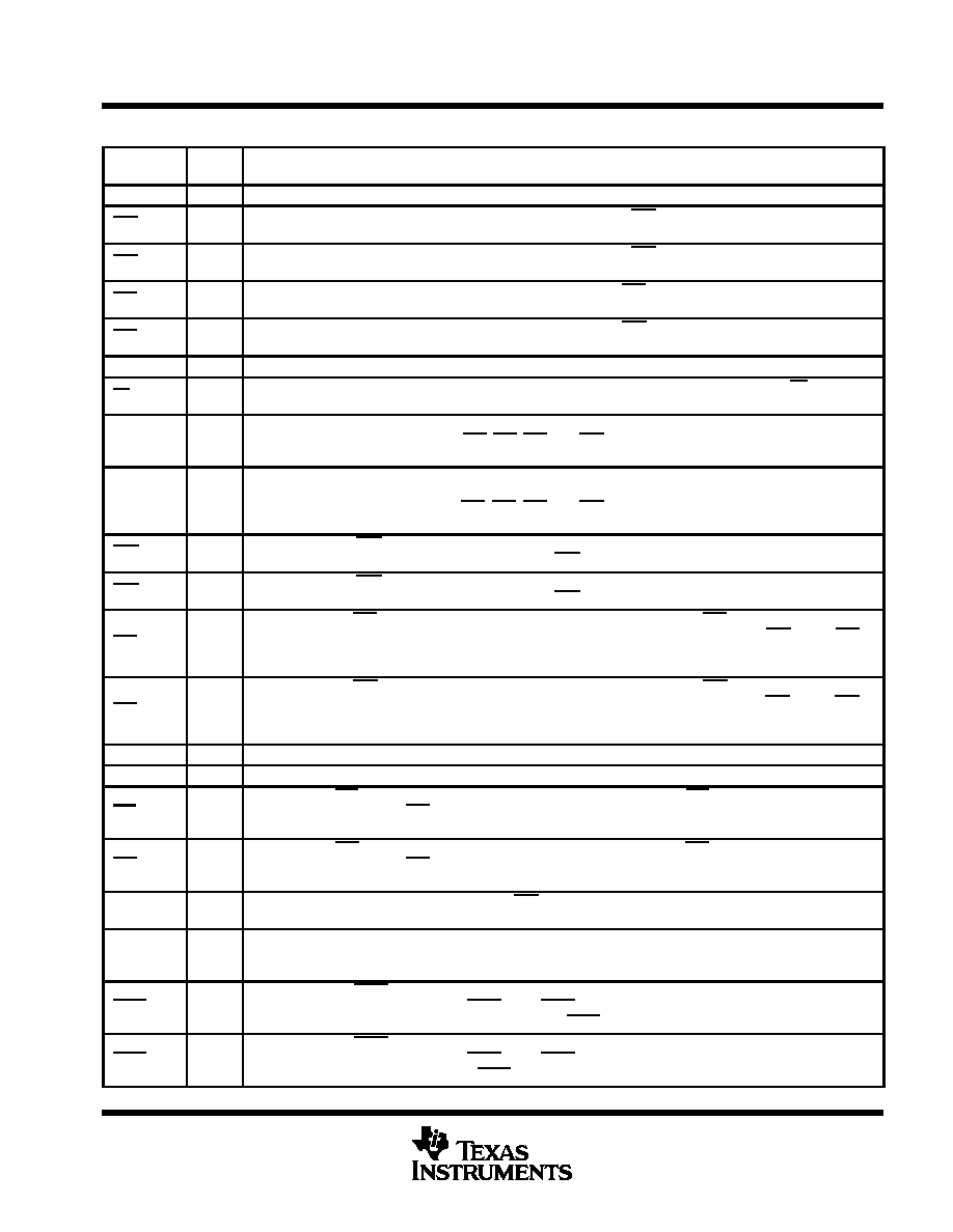
Terminal Functions
TERMINAL
NAME
I/O
DESCRIPTION
A0≠A35
I/O
Port-A data. The 36-bit bidirectional data port for side A.
AEA
O
(port A)
Port-A almost-empty flag. Programmable flag synchronized to CLKA. AEA is low when the number of 36-bit words
in FIFO2 is less than or equal to value in offset register X.
AEB
O
(port B)
Port-B almost-empty flag. Programmable flag synchronized to CLKB. AEB is low when the number of 36-bit words
in FIFO1 is less than or equal to value in offset register X.
AFA
O
(port A)
Port-A almost-full flag. Programmable flag synchronized to CLKA. AFA is low when the number of 36-bit empty
locations in FIFO1 is less than or equal to the value in offset register X.
AFB
O
(port B)
Port-B almost-full flag. Programmable flag synchronized to CLKB. AFB is low when the number of 36-bit empty
locations in FIFO2 is less than or equal to the value in offset register X.
B0≠B35
I/O
Port-B data. The 36-bit bidirectional data port for side B.
BE
I
Big-endian select. Selects the bytes on port B used during byte or word data transfer. A low on BE selects the
most-significant bytes on B0≠B35 for use, and a high selects the least-significant bytes.
CLKA
I
Port-A clock. CLKA is a continuous clock that synchronizes all data transfers through port A and can be
asynchronous or coincident to CLKB. EFA, FFA, AFA, and AEA are synchronized to the low-to-high transition of
CLKA.
CLKB
I
Port-B clock. CLKB is a continuous clock that synchronizes all data transfers through port B and can be
asynchronous or coincident to CLKA. Port-B byte swapping and data-port sizing operations are also synchronous
to the low-to-high transition of CLKB. EFB, FFB, AFB, and AEB are synchronized to the low-to-high transition of
CLKB.
CSA
I
Port-A chip select. CSA must be low to enable a low-to-high transition of CLKA to read or write data on port A. The
A0≠A35 outputs are in the high-impedance state when CSA is high.
CSB
I
Port-B chip select. CSB must be low to enable a low-to-high transition of CLKB to read or write data on port B. The
B0≠B35 outputs are in the high-impedance state when CSB is high.
EFA
O
(port A)
Port-A empty flag. EFA is synchronized to the low-to-high transition of CLKA. When EFA is low, FIFO2 is empty and
reads from its memory are disabled. Data can be read from FIFO2 to the output register when EFA is high. EFA is
forced low when the device is reset and is set high by the second low-to-high transition of CLKA after data is loaded
into empty FIFO2 memory.
EFB
O
(port B)
Port-B empty flag. EFB is synchronized to the low-to-high transition of CLKB. When EFB is low, FIFO1 is empty and
reads from its memory are disabled. Data can be read from FIFO1 to the output register when EFB is high. EFB is
forced low when the device is reset and is set high by the second low-to-high transition of CLKB after data is loaded
into empty FIFO1 memory.
ENA
I
Port-A enable. ENA must be high to enable a low-to-high transition of CLKA to read or write data on port A.
ENB
I
Port-B enable. ENB must be high to enable a low-to-high transition of CLKB to read or write data on port B.
FFA
O
(port A)
Port-A full flag. FFA is synchronized to the low-to-high transition of CLKA. When FFA is low, FIFO1 is full and writes
to its memory are disabled. FFA is forced low when the device is reset and is set high by the second low-to-high
transition of CLKA after reset.
FFB
O
(port B)
Port-B full flag. FFB is synchronized to the low-to-high transition of CLKB. When FFB is low, FIFO2 is full and writes
to its memory are disabled. FFB is forced low when the device is reset and is set high by the second low-to-high
transition of CLKB after reset.
FS1, FS0
I
Flag offset selects. The low-to-high transition of RST latches the values of FS0 and FS1, which selects one of four
preset values for the almost-empty flag and almost-full flag offset.
MBA
I
Port-A mailbox select. A high level on MBA chooses a mailbox register for a port-A read or write operation. When
the A0≠A35 outputs are active, a high level on MBA selects data from the mail2 register for output and a low level
selects FIFO2 output register data for output.
MBF1
O
Mail1 register flag. MBF1 is set low by the low-to-high transition of CLKA that writes data to the mail1 register. Writes
to the mail1 register are inhibited while MBF1 is low. MBF1 is set high by a low-to-high transition of CLKB when a
port-B read is selected and both SIZ1 and SIZ0 are high. MBF1 is set high when the device is reset.
MBF2
O
Mail2 register flag. MBF2 is set low by the low-to-high transition of CLKB that writes data to the mail2 register. Writes
to the mail2 register are inhibited while MBF2 is low. MBF2 is set high by a low-to-high transition of CLKA when a
port-A read is selected and MBA is high. MBF2 is set high when the device is reset.