
TLC225x, TLC225xA
Advanced LinCMOS
RAIL-TO-RAIL
VERY LOW-POWER OPERATIONAL AMPLIFIERS
SLOS176D ≠ FEBRUARY 1997 ≠ REVISED MARCH 2001
1
POST OFFICE BOX 655303
∑
DALLAS, TEXAS 75265
D
Output Swing Includes Both Supply Rails
D
Low Noise . . . 19 nV/
Hz Typ at f = 1 kHz
D
Low Input Bias Current . . . 1 pA Typ
D
Fully Specified for Both Single-Supply and
Split-Supply Operation
D
Very Low Power . . . 35
µ
A Per Channel Typ
D
Common-Mode Input Voltage Range
Includes Negative Rail
D
Low Input Offset Voltage
850
µ
V Max at T
A
= 25
∞
C (TLC225xA)
D
Macromodel Included
D
Performance Upgrades for the TS27L2/L4
and TLC27L2/L4
D
Available in Q≠Temp Automotive
HighRel Automotive Applications
Configuration Control / Print Support
Qualification to Automotive Standards
description
The TLC2252 and TLC2254 are dual and
quadruple operational amplifiers from Texas
Instruments. Both devices exhibit rail-to-rail
output performance for increased dynamic range
in single- or split-supply applications. The
TLC225x family consumes only 35
µ
A of supply
current per channel. This micropower operation
makes them good choices for battery-powered
applications. The noise performance has been
dramatically improved over previous generations
of CMOS amplifiers. Looking at Figure 1, the
TLC225x has a noise level of 19 nV/
Hz at 1kHz;
four times lower than competitive micropower
solutions.
The TLC225x amplifiers, exhibiting high input
impedance and low noise, are excellent for
small-signal conditioning for high-impedance
sources, such as piezoelectric transducers.
Because of the micropower dissipation levels,
these devices work well in hand-held monitoring
and remote-sensing applications. In addition, the
rail-to-rail output feature with single or split
supplies makes this family a great choice when interfacing with analog-to-digital converters (ADCs). For
precision applications, the TLC225xA family is available and has a maximum input offset voltage of 850
µ
V. This
family is fully characterized at 5 V and
±
5 V.
The TLC2252/4 also makes great upgrades to the TLC27L2/L4 or TS27L2/L4 in standard designs. They offer
increased output dynamic range, lower noise voltage, and lower input offset voltage. This enhanced feature set
allows them to be used in a wider range of applications. For applications that require higher output drive and
wider input voltage ranges, see the TLV2432 and TLV2442 devices. If the design requires single amplifiers,
please see the TLV2211/21/31 family. These devices are single rail-to-rail operational amplifiers in the SOT-23
package. Their small size and low power consumption, make them ideal for high density, battery-powered
equipment.
Copyright
2001, Texas Instruments Incorporated
PRODUCTION DATA information is current as of publication date.
Products conform to specifications per the terms of Texas Instruments
standard warranty. Production processing does not necessarily include
testing of all parameters.
Please be aware that an important notice concerning availability, standard warranty, and use in critical applications of
Texas Instruments semiconductor products and disclaimers thereto appears at the end of this data sheet.
Advanced LinCMOS is a trademark of Texas Instruments.
Figure 1
VN ≠ Equivalent Input Noise V
oltage ≠ nv//Hz
f ≠ Frequency ≠ Hz
EQUIVALENT INPUT NOISE VOLTAGE
vs
FREQUENCY
nV/
Hz
V
n
40
20
10
0
60
30
50
101
10 2
10 3
10 4
VDD = 5 V
RS = 20
TA = 25
∞
C
On products compliant to MIL-PRF-38535, all parameters are tested
unless otherwise noted. On all other products, production
processing does not necessarily include testing of all parameters.
TLC225x, TLC225xA
Advanced LinCMOS
RAIL-TO-RAIL
VERY LOW-POWER OPERATIONAL AMPLIFIERS
SLOS176D ≠ FEBRUARY 1997 ≠ REVISED MARCH 2001
2
POST OFFICE BOX 655303
∑
DALLAS, TEXAS 75265
TLC2252 AVAILABLE OPTIONS
PACKAGED DEVICES
TA
VIOmax
AT 25
∞
C
SMALL
OUTLINE
(D)
CHIP
CARRIER
(FK)
CERAMIC
DIP
(JG)
PLASTIC
DIP
(P)
TSSOP
(PW)
CERAMIC
FLATPACK
(U)
0
∞
C to 70
∞
C
1500
µ
V
TLC2252CD
--
--
TLC2252CP
TLC2252CPW
--
40
∞
C to 125
∞
C
850
µ
V
TLC2252AID
--
--
TLC2252AIP
TLC2252AIPW
--
≠ 40
∞
C to 125
∞
C
µ
1500
µ
V
TLC2252ID
--
--
TLC2252IP
--
--
40
∞
C to 125
∞
C
850
µ
V
TLC2252AQD
--
--
--
--
--
≠ 40
∞
C to 125
∞
C
µ
1500
µ
V
TLC2252QD
--
--
--
--
--
≠ 55
∞
C to 125
∞
C
850
µ
V
1500
µ
V
--
--
TLC2252AMFK
TLC2252MFK
TLC2252AMJG
TLC2252MJG
--
--
--
--
TLC2252AMU
TLC2252MU
The D packages are available taped and reeled. Add R suffix to device type (e.g., TLC2262CDR).
The PW package is available only left-ended taped and reeled.
ß Chip forms are tested at 25
∞
C only.
TLC2254 AVAILABLE OPTIONS
PACKAGED DEVICES
TA
VIOmax
AT 25
∞
C
SMALL
OUTLINE
(D)
CHIP
CARRIER
(FK)
CERAMIC
DIP
(J)
PLASTIC DIP
(N)
TSSOP
(PW)
CERAMIC
FLATPACK
(W)
0
∞
C to
70
∞
C
1500
µ
V
TLC2254CD
--
--
TLC2254CN
TLC2254CPW
--
≠ 40
∞
C to
850
µ
V
TLC2254AID
--
--
TLC2254AIN
TLC2254AIPW
--
125
∞
C
µ
1500
µ
V
TLC2254ID
--
--
TLC2254IN
--
--
≠ 40
∞
C to
850
µ
V
TLC2254AQD
--
--
--
--
--
125
∞
C
µ
1500
µ
V
TLC2254QD
--
--
--
--
--
≠ 55
∞
C to
850
µ
V
--
TLC2254AMFK
TLC2254AMJ
--
--
TLC2254AMW
125
∞
C
µ
1500
µ
V
--
TLC2254MFK
TLC2254MJ
--
--
TLC2254MW
The D packages are available taped and reeled. Add R suffix to the device type (e.g., TLC2254CDR).
The PW package is available only left-end taped and reeled. Chips are tested at 25
∞
C.
ß Chip forms are tested at 25
∞
C only.

TLC225x, TLC225xA
Advanced LinCMOS
RAIL-TO-RAIL
VERY LOW-POWER OPERATIONAL AMPLIFIERS
SLOS176D ≠ FEBRUARY 1997 ≠ REVISED MARCH 2001
3
POST OFFICE BOX 655303
∑
DALLAS, TEXAS 75265
TLC2252M, TLC2252AM . . . JG PACKAGE
(TOP VIEW)
TLC2252C, TLC2252AC
TLC2252I, TLC2252AI
TLC2252Q, TLC2252AQ
D, P, OR PW PACKAGE
(TOP VIEW)
1
2
3
4
8
7
6
5
1OUT
1IN ≠
1IN +
V
DD ≠
/GND
V
DD +
2OUT
2IN ≠
2IN +
NC
V
CC
+
2OUT
2IN ≠
2IN +
NC
1OUT
1IN ≠
1IN +
V
CC ≠
/GND
1
2
3
4
5
10
9
8
7
6
TLC2262M, TLC2252AM . . . U PACKAGE
(TOP VIEW)
1
2
3
4
8
7
6
5
1OUT
1IN ≠
1IN +
V
DD ≠
/GND
V
DD +
2OUT
2IN ≠
2IN +
3
2
1 20 19
9 10 11 12 13
4
5
6
7
8
18
17
16
15
14
NC
2OUT
NC
2IN ≠
NC
NC
1IN ≠
NC
1IN +
NC
NC
1OUT
NC
2IN+
NC
NC
NC
NC
V
DD+
V
DD
≠
TLC2252M, TLC2252AM . . . FK PACKAGE
(TOP VIEW)
/GND
1
2
3
4
5
6
7
14
13
12
11
10
9
8
1OUT
1IN ≠
1IN +
V
DD +
2IN +
2IN ≠
2OUT
4OUT
4IN ≠
4IN +
V
DD ≠
/ GND
3IN +
3IN ≠
3OUT
3
2
1 20 19
9 10 11 12 13
4
5
6
7
8
18
17
16
15
14
4IN +
NC
V
CC ≠
/GND
NC
3IN +
1IN +
NC
V
CC +
NC
2IN +
1IN
≠
1OUT
NC
3OUT
3IN
≠
4OUT
4IN
≠
2IN
≠
2OUT
NC
TLC2254M, TLC2254AM
FK PACKAGE
(TOP VIEW)
TLC2254C, TLC2254AC
TLC2254I, TLC2254AI
TLC2254Q, TLC2254AQ
D, N, OR PW PACKAGE
(TOP VIEW)
1
2
3
4
5
6
7
14
13
12
11
10
9
8
1OUT
1IN ≠
1IN +
V
DD +
2IN +
2IN ≠
2OUT
4OUT
4IN ≠
4IN +
V
DD ≠
/ GND
3IN +
3IN ≠
3OUT
TLC2254M, TLC2254AM
J OR W PACKAGE
(TOP VIEW)
NC ≠ No internal connection

TLC225x, TLC225xA
Advanced LinCMOS
RAIL-TO-RAIL
VERY LOW-POWER OPERATIONAL AMPLIFIERS
SLOS176D ≠ FEBRUARY 1997 ≠ REVISED MARCH 2001
4
POST OFFICE BOX 655303
∑
DALLAS, TEXAS 75265
equivalent schematic (each amplifier)
Q3
Q6
Q9
Q12
Q14
Q16
Q2
Q5
Q7
Q8
Q10
Q11
D1
Q17
Q15
Q13
Q4
Q1
R5
C1
VDD +
IN +
IN ≠
R3
R4
R1
R2
OUT
VDD ≠ / GND
R6
ACTUAL DEVICE COMPONENT COUNT
COMPONENT
TLC2252
TLC2254
Transistors
38
76
Resistors
30
56
Diodes
9
18
Capacitors
3
6
Includes both amplifiers and all ESD, bias, and trim circuitry

TLC225x, TLC225xA
Advanced LinCMOS
RAIL-TO-RAIL
VERY LOW-POWER OPERATIONAL AMPLIFIERS
SLOS176D ≠ FEBRUARY 1997 ≠ REVISED MARCH 2001
5
POST OFFICE BOX 655303
∑
DALLAS, TEXAS 75265
absolute maximum ratings over operating free-air temperature range (unless otherwise noted)
Supply voltage, V
DD +
(see Note 1)
8 V
. . . . . . . . . . . . . . . . . . . . . . . . . . . . . . . . . . . . . . . . . . . . . . . . . . . . . . . . . . . .
Supply voltage, V
DD ≠
(see Note 1)
≠ 8 V
. . . . . . . . . . . . . . . . . . . . . . . . . . . . . . . . . . . . . . . . . . . . . . . . . . . . . . . . . . .
Differential input voltage, V
ID
(see Note 2)
±
16 V
. . . . . . . . . . . . . . . . . . . . . . . . . . . . . . . . . . . . . . . . . . . . . . . . . . .
Input voltage, V
I
(any input, see Note 1)
±
8 V
. . . . . . . . . . . . . . . . . . . . . . . . . . . . . . . . . . . . . . . . . . . . . . . . . . . . . .
Input current, I
I
(each input)
±
5 mA
. . . . . . . . . . . . . . . . . . . . . . . . . . . . . . . . . . . . . . . . . . . . . . . . . . . . . . . . . . . . . . .
Output current, I
O
±
50 mA
. . . . . . . . . . . . . . . . . . . . . . . . . . . . . . . . . . . . . . . . . . . . . . . . . . . . . . . . . . . . . . . . . . . . . . .
Total current into V
DD +
±
50 mA
. . . . . . . . . . . . . . . . . . . . . . . . . . . . . . . . . . . . . . . . . . . . . . . . . . . . . . . . . . . . . . . . . .
Total current out of V
DD ≠
±
50 mA
. . . . . . . . . . . . . . . . . . . . . . . . . . . . . . . . . . . . . . . . . . . . . . . . . . . . . . . . . . . . . . . .
Duration of short-circuit current at (or below) 25
∞
C (see Note 3)
unlimited
. . . . . . . . . . . . . . . . . . . . . . . . . . . . . .
Continuous total dissipation
See Dissipation Rating Table
. . . . . . . . . . . . . . . . . . . . . . . . . . . . . . . . . . . . . . . . . . .
Operating free-air temperature range, T
A
: C suffix
0
∞
C to 70
∞
C
. . . . . . . . . . . . . . . . . . . . . . . . . . . . . . . . . . . . . .
I suffix
≠ 40
∞
C to 125
∞
C
. . . . . . . . . . . . . . . . . . . . . . . . . . . . . . . . . . . .
Q suffix
≠ 40
∞
C to 125
∞
C
. . . . . . . . . . . . . . . . . . . . . . . . . . . . . . . . . . .
M suffix
≠ 55
∞
C to 125
∞
C
. . . . . . . . . . . . . . . . . . . . . . . . . . . . . . . . . .
Storage temperature range, T
stg
≠ 65
∞
C to 150
∞
C
. . . . . . . . . . . . . . . . . . . . . . . . . . . . . . . . . . . . . . . . . . . . . . . . . . .
Lead temperature 1,6 mm (1/16 inch) from case for 10 seconds
260
∞
C
. . . . . . . . . . . . . . . . . . . . . . . . . . . . . . .
Stresses beyond those listed under "absolute maximum ratings" may cause permanent damage to the device. These are stress ratings only, and
functional operation of the device at these or any other conditions beyond those indicated under "recommended operating conditions" is not
implied. Exposure to absolute-maximum-rated conditions for extended periods may affect device reliability.
NOTES:
1. All voltage values, except differential voltages, are with respect to the midpoint between VDD+ and VDD ≠ .
2. Differential voltages are at IN+ with respect to IN ≠. Excessive current flows when input is brought below VDD ≠ ≠ 0.3 V.
3. The output may be shorted to either supply. Temperature and/or supply voltages must be limited to ensure that the maximum
dissipation rating is not exceeded.
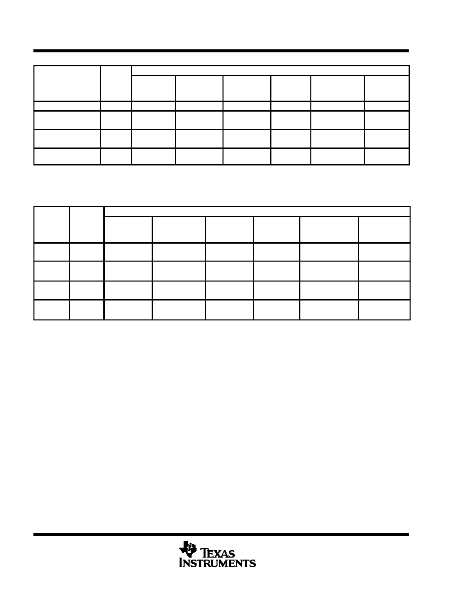
DISSIPATION RATING TABLE
PACKAGE
TA
25
∞
C
DERATING FACTOR
TA = 70
∞
C
TA = 85
∞
C
TA = 125
∞
C
PACKAGE
A
POWER RATING
ABOVE TA = 25
∞
C
A
POWER RATING
A
POWER RATING
A
POWER RATING
D≠8
724 mW
5.8 mW/
∞
C
464 mW
377 mW
144 mW
D≠14
950 mW
7.6 mW/
∞
C
608 mW
450 mW
190 mW
FK
1375 mW
11.0 mW/
∞
C
880 mW
715 mW
275 mW
J
1375 mW
11.0 mW/
∞
C
880 mW
715 mW
275 mW
JG
1050 mW
8.4 mW/
∞
C
672 mW
546 mW
275 mW
N
1150 mW
9.2 mW/
∞
C
736 mW
736 mW
--
P
1000 mW
8.0 mW/
∞
C
640 mW
520 mW
--
PW≠8
525 mW
4.2 mW/
∞
C
336 mW
273 mW
--
PW≠14
700 mW
5.6 mW/
∞
C
448 mW
448 mW
--
U
700 mW
5.5 mW/
∞
C
246 mW
330 mW
150 mW
W
700 mW
5.5 mW/
∞
C
246 mW
330 mW
150 mW
recommended operating conditions
C SUFFIX
I SUFFIX
Q SUFFIX
M SUFFIX
UNIT
MIN
MAX
MIN
MAX
MIN
MAX
MIN
MAX
UNIT
Supply voltage, VDD
±
±
2.2
±
8
±
2.2
±
8
±
2.2
±
8
±
2.2
±
8
V
Input voltage range, VI
VDD ≠ VDD + ≠ 1.5 VDD ≠ VDD + ≠ 1.5 VDD ≠ VDD + ≠ 1.5 VDD ≠ VDD + ≠ 1.5
V
Common-mode input voltage, VIC
VDD ≠ VDD + ≠ 1.5 VDD ≠ VDD + ≠ 1.5 VDD ≠ VDD + ≠ 1.5 VDD ≠ VDD + ≠ 1.5
V
Operating free-air temperature, TA
0
70
≠ 40
125
≠ 40
125
≠ 55
125
∞
C