
SN54ABTH18646A, SN54ABTH182646A, SN74ABTH18646A, SN74ABTH182646A
SCAN TEST DEVICES WITH
18-BIT TRANSCEIVERS AND REGISTERS
SCBS166D ≠ AUGUST 1993 ≠ REVISED JULY 1996
1
POST OFFICE BOX 655303
∑
DALLAS, TEXAS 75265
D
Members of the Texas Instruments
SCOPE
TM
Family of Testability Products
D
Members of the Texas Instruments
Widebus
TM
Family
D
Compatible With the IEEE Standard
1149.1-1990 (JTAG) Test Access Port and
Boundary-Scan Architecture
D
Include D-Type Flip-Flops and Control
Circuitry to Provide Multiplexed
Transmission of Stored and Real-Time Data
D
Bus Hold on Data Inputs Eliminates the
Need for External Pullup Resistors
D
B-Port Outputs of 'ABTH182646A Devices
Have Equivalent 25-
Series Resistors, So
No External Resistors Are Required
D
State-of-the-Art
EPIC-
B
TM
BiCMOS Design
D
One Boundary-Scan Cell Per I/O
Architecture Improves Scan Efficiency
D
SCOPE
TM
Instruction Set
≠ IEEE Standard 1149.1-1990 Required
Instructions and Optional CLAMP and
HIGHZ
≠ Parallel-Signature Analysis at Inputs
≠ Pseudo-Random Pattern Generation
From Outputs
≠ Sample Inputs/Toggle Outputs
≠ Binary Count From Outputs
≠ Device Identification
≠ Even-Parity Opcodes
D
Packaged in 64-Pin Plastic Thin Quad Flat
(PM) Packages Using 0.5-mm
Center-to-Center Spacings and 68-Pin
Ceramic Quad Flat (HV) Packages Using
25-mil Center-to-Center Spacings
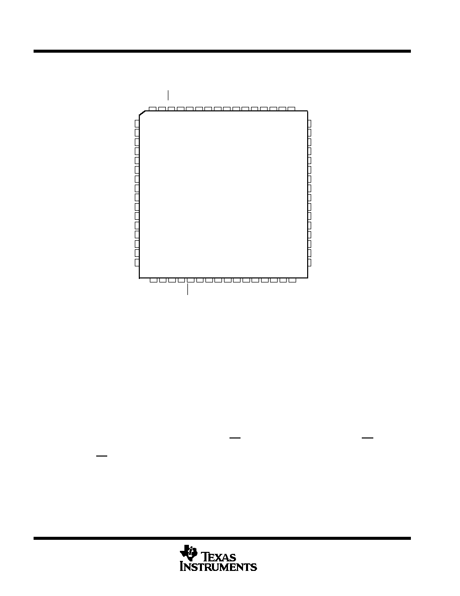
1B4
1B5
1B6
GND
1B7
1B8
1B9
V
CC
NC
2B1
2B2
2B3
2B4
GND
2B5
2B6
2B7
1A3
1A4
1A5
GND
1A6
1A7
1A8
1A9
NC
V
CC
2A1
2A2
2A3
GND
2A4
2A5
2A6
V
NC
TMS
1CLKBA
1A2
1A1
1OE
GND
1SAB
1CLKAB
TDO
NC
TCK
2CLKBA
2SBA
2A9
GND
2OE
2SAB
2CLKAB
TDI
2A7
2A8
1SBA
1DIR
GND
2DIR
2B9
2B8
GND
1B1
1B2
1B3
28 29
60
59
58
57
56
55
54
53
52
51
50
49
48
47
46
45
44
30
10
11
12
13
14
15
16
17
18
19
20
21
22
23
24
25
26
31 32 33 34
8 7
6
5
4
9
3
1 68 67
2
35 36 37 38 39
66 65
27
64 63 62 61
40 41 42 43
SN54ABTH18646A, SN54ABTH182646A . . . HV PACKAGE
(TOP VIEW)
CC
V
CC
NC ≠ No internal connection
Copyright
©
1996, Texas Instruments Incorporated
UNLESS OTHERWISE NOTED this document contains PRODUCTION
DATA information current as of publication date. Products conform to
specifications per the terms of Texas Instruments standard warranty.
Production processing does not necessarily include testing of all
parameters.
Please be aware that an important notice concerning availability, standard warranty, and use in critical applications of
Texas Instruments semiconductor products and disclaimers thereto appears at the end of this data sheet.
SCOPE, Widebus, and EPIC-
B are trademarks of Texas Instruments Incorporated.
On products compliant to MIL-PRF-38535, all parameters are tested
unless otherwise noted. On all other products, production
processing does not necessarily include testing of all parameters.
SN54ABTH18646A, SN54ABTH182646A, SN74ABTH18646A, SN74ABTH182646A
SCAN TEST DEVICES WITH
18-BIT TRANSCEIVERS AND REGISTERS
SCBS166D ≠ AUGUST 1993 ≠ REVISED JULY 1996
2
POST OFFICE BOX 655303
∑
DALLAS, TEXAS 75265
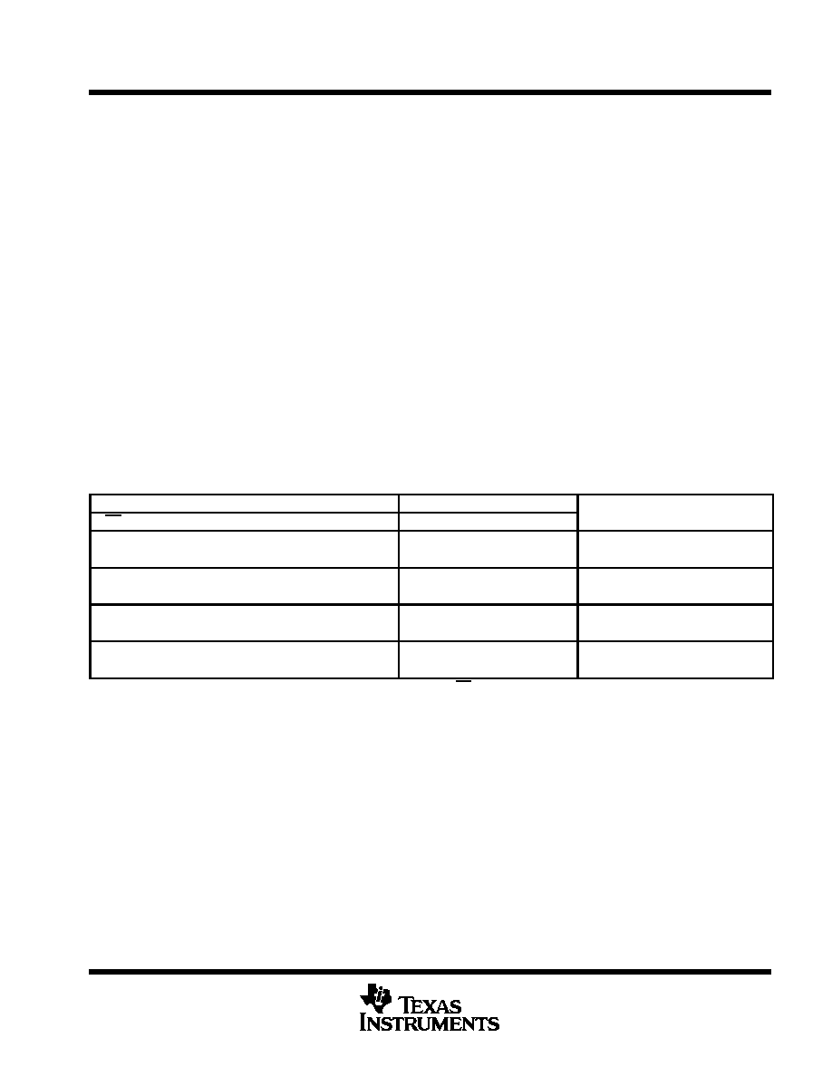
2A9
GND
2SAB
2CLKAB
2A7
2A8
2OE
TDI
2CLKBA
2SBA
2DIR
2B9
V
TCK
GND
2B8
CC
18 19
48
47
46
45
44
43
42
41
40
39
38
37
36
35
34
33
20
1
2
3
4
5
6
7
8
9
10
11
12
13
14
15
16
21 22 23 24
63 62 61 60 59
64
58
56 55 54
57
25 26 27 28 29
53 52
17
51 50 49
30 31 32
1OE
GND
1CLKAB
TDO
1A2
1A1
1SAB
V
1SBA
1DIR
1B1
1B2
TMS
1CLKBA
GND
1B3
1A3
1A4
1A5
GND
1A6
1A7
1A8
1A9
V
CC
2A1
2A2
2A3
GND
2A4
2A5
2A6
1B4
1B5
1B6
GND
1B7
1B8
1B9
V
CC
2B1
2B2
2B3
2B4
GND
2B5
2B6
2B7
CC
SN74ABTH18646A, SN74ABTH182646A . . . PM PACKAGE
(TOP VIEW)
description
The 'ABTH18646A and 'ABTH182646A scan test devices with 18-bit bus transceivers and registers are
members of the Texas Instruments SCOPE
TM
testability integrated-circuit family. This family of devices supports
IEEE Standard 1149.1-1990 boundary scan to facilitate testing of complex circuit-board assemblies. Scan
access to the test circuitry is accomplished via the 4-wire test access port (TAP) interface.
In the normal mode, these devices are 18-bit bus transceivers and registers that allow for multiplexed
transmission of data directly from the input bus or from the internal registers. They can be used either as two
9-bit transceivers or one 18-bit transceiver. The test circuitry can be activated by the TAP to take snapshot
samples of the data appearing at the device pins or to perform a self test on the boundary-test cells. Activating
the TAP in the normal mode does not affect the functional operation of the SCOPE
TM
bus transceivers and
registers.
Transceiver function is controlled by output-enable (OE) and direction (DIR) inputs. When OE is low, the
transceiver is active and operates in the A-to-B direction when DIR is high or in the B-to-A direction when DIR
is low. When OE is high, both the A and B outputs are in the high-impedance state, effectively isolating both
buses.
Data flow is controlled by clock (CLKAB and CLKBA) and select (SAB and SBA) inputs. Data on the A bus is
clocked into the associated registers on the low-to-high transition of CLKAB. When SAB is low, real-time A data
is selected for presentation to the B bus (transparent mode). When SAB is high, stored A data is selected for
presentation to the B bus (registered mode). The function of the CLKBA and SBA inputs mirrors that of CLKAB
and SAB, respectively. Figure 1 shows the four fundamental bus-management functions that are performed with
the 'ABTH18646A and 'ABTH182646A.
SN54ABTH18646A, SN54ABTH182646A, SN74ABTH18646A, SN74ABTH182646A
SCAN TEST DEVICES WITH
18-BIT TRANSCEIVERS AND REGISTERS
SCBS166D ≠ AUGUST 1993 ≠ REVISED JULY 1996
3
POST OFFICE BOX 655303
∑
DALLAS, TEXAS 75265
description (continued)
In the test mode, the normal operation of the SCOPE
TM
bus transceivers and registers is inhibited, and the test
circuitry is enabled to observe and control the I/O boundary of the device. When enabled, the test circuitry
performs boundary-scan test operations according to the protocol described in IEEE Standard 1149.1-1990.
Four dedicated test pins observe and control the operation of the test circuitry: test data input (TDI), test data
output (TDO), test mode select (TMS), and test clock (TCK). Additionally, the test circuitry performs other testing
functions such as parallel-signature analysis (PSA) on data inputs and pseudo-random pattern generation
(PRPG) from data outputs. All testing and scan operations are synchronized to the TAP interface.
Improved scan efficiency is accomplished through the adoption of a one boundary-scan cell (BSC) per I/O pin
architecture. This architecture is implemented in such a way as to capture the most pertinent test data. A
PSA/COUNT instruction also is included to ease the testing of memories and other circuits where a binary count
addressing scheme is useful.
Active bus-hold circuitry holds unused or floating data inputs at a valid logic level.
The B-port outputs of 'ABTH182646A, which are designed to source or sink up to 12 mA, include 25-
series
resistors to reduce overshoot and undershoot.
The SN54ABTH18646A and SN54ABTH182646A are characterized for operation over the full military
temperature range of ≠55
∞
C to 125
∞
C. The SN74ABTH18646A and SN74ABTH182646A are characterized for
operation from ≠40
∞
C to 85
∞
C.
FUNCTION TABLE
(normal mode, each 9-bit section)
INPUTS
DATA I/O
OPERATION OR FUNCTION
OE
DIR
CLKAB
CLKBA
SAB
SBA
A1 ≠ A9
B1 ≠ B9
OPERATION OR FUNCTION
X
X
X
X
X
Input
Unspecified
Store A, B unspecified
X
X
X
X
X
Unspecified
Input
Store B, A unspecified
H
X
X
X
Input
Input
Store A and B data
H
X
L
L
X
X
Input disabled
Input disabled
Isolation, hold storage
L
L
X
X
X
L
Output
Input
Real-time B data to A bus
L
L
X
X
X
H
Output
Input disabled
Stored B data to A bus
L
H
X
X
L
X
Input
Output
Real-time A data to B bus
L
H
X
X
H
X
Input disabled
Output
Stored A data to B bus
The data-output functions can be enabled or disabled by various signals at OE and DIR. Data-input functions are always enabled; i.e., data at
the bus pins is stored on every low-to-high transition of the clock inputs.

SN54ABTH18646A, SN54ABTH182646A, SN74ABTH18646A, SN74ABTH182646A
SCAN TEST DEVICES WITH
18-BIT TRANSCEIVERS AND REGISTERS
SCBS166D ≠ AUGUST 1993 ≠ REVISED JULY 1996
4
POST OFFICE BOX 655303
∑
DALLAS, TEXAS 75265
L
DIR
L
CLKAB
X
CLKBA
X
SAB
X
SBA
L
REAL-TIME TRANSFER
BUS B TO BUS A
L
DIR
H
CLKAB
X
CLKBA
X
SAB
L
SBA
X
REAL-TIME TRANSFER
BUS A TO BUS B
X
DIR
X
CLKAB CLKBA
X
SAB
X
SBA
X
STORAGE FROM
A, B, OR A AND B
L
DIR
L
CLKAB
X
CLKBA
X
SAB
X
SBA
H
TRANSFER STORED DATA
TO A AND/OR B
X
H
X
X
X
X
X
X
X
L
H
X
X
H
X
BUS B
BUS A
BUS B
BUS A
BUS B
BUS A
BUS B
BUS A
OE
OE
OE
OE
Figure 1. Bus-Management Functions

SN54ABTH18646A, SN54ABTH182646A, SN74ABTH18646A, SN74ABTH182646A
SCAN TEST DEVICES WITH
18-BIT TRANSCEIVERS AND REGISTERS
SCBS166D ≠ AUGUST 1993 ≠ REVISED JULY 1996
5
POST OFFICE BOX 655303
∑
DALLAS, TEXAS 75265
functional block diagram
Boundary-Scan Register
One of Nine Channels
1OE
1DIR
1CLKBA
1SBA
1CLKAB
1SAB
1A1
1B1
1D
C1
1D
C1
One of Nine Channels
2OE
2DIR
2CLKBA
2SBA
2CLKAB
2SAB
2A1
2B1
1D
C1
1D
C1
Boundary-Control
Register
Instruction
Register
TDI
TMS
TCK
TDO
TAP
Controller
VCC
VCC
Bypass Register
Identification
Register
62
53
55
54
59
60
63
21
30
27
28
23
22
10
24
56
26
51
40
58
VCC
VCC
Pin numbers shown are for the PM package.