"Dual Asychronous Communications Element With FIFO"
TL16C552A, TL16C552AM
DUAL ASYNCHRONOUS COMMUNICATIONS ELEMENT
WITH FIFO
SLLS189D NOVEMBER 1994 REVISED JANUARY 1999
1
POST OFFICE BOX 655303
·
DALLAS, TEXAS 75265
D
IBM PC/AT
TM
Compatible
D
Two TL16C550 ACEs
D
Enhanced Bidirectional Printer Port
D
16-Byte FIFOs Reduce CPU Interrupts
D
Up to 16-MHz Clock Rate for up to 1-Mbaud
Operation
D
Transmit, Receive, Line Status, and Data
Set Interrupts on Each Channel
Independently Controlled
D
Individual Modem Control Signals for Each
Channel
D
Programmable Serial Interface
Characteristics for Each Channel:
5-, 6-, 7-, or 8-Bit Characters
Even, Odd, or No Parity Bit Generation
and Detection
1-, 1-1/2-, or 2-Stop Bit Generation
D
3-State Outputs Provide TTL Drive for the
Data and Control Bus on Each Channel
D
Hardware and Software Compatible With
TL16C452
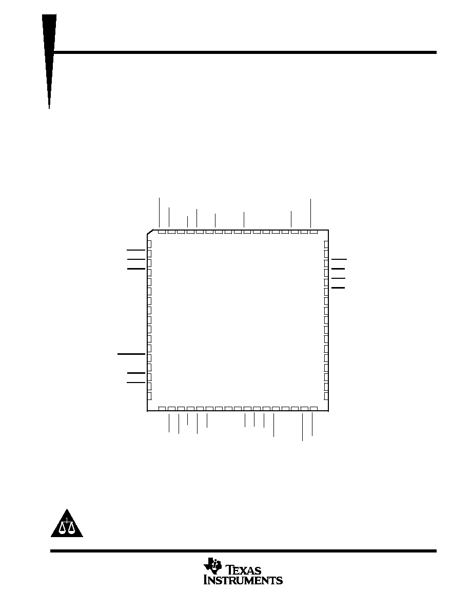
28 29
INT1
INT2
SLIN
INIT
AFD
STB
GND
PD0
PD1
PD2
PD3
PD4
PD5
PD6
PD7
INT0
BDO
60
59
58
57
56
55
54
53
52
51
50
49
48
47
46
45
44
30
10
11
12
13
14
15
16
17
18
19
20
21
22
23
24
25
26
SOUT1
DTR1
RTS1
CTS1
DB0
DB1
DB2
DB3
DB4
DB5
DB6
DB7
TXRDY0
V
DD
RTS0
DTR0
SOUT0
31 32 33 34
HV or FN PACKAGE
(TOP VIEW)
ACK
PE
8 7
6
5
4
9
3
GND
RI1
DSR1
CLK
CS1
TRI
PEMD
IOW
IOR
CS2
RESET
DCD0
RI0
DSR0
CS0
A2
A1
A0
1 68 67
2
35 36 37 38 39
66 65
27
GND
CTS0
BUSY
SLCT
64 63 62 61
40 41 42 43
SIN0
TXRDY1
ENIRQ
ERR
SIN1
RXRDY1
RXRDY0
DCD1
V
DD
V
DD
Please be aware that an important notice concerning availability, standard warranty, and use in critical applications of
Texas Instruments semiconductor products and disclaimers thereto appears at the end of this data sheet.
PRODUCTION DATA information is current as of publication date.
Products conform to specifications per the terms of Texas Instruments
standard warranty. Production processing does not necessarily include
testing of all parameters.
Copyright
©
1999, Texas Instruments Incorporated
IBM PC/AT is a trademark of International Business Machines Corporation.
TL16C552A, TL16C552AM
DUAL ASYNCHRONOUS COMMUNICATIONS ELEMENT
WITH FIFO
SLLS189D NOVEMBER 1994 REVISED JANUARY 1999
2
POST OFFICE BOX 655303
·
DALLAS, TEXAS 75265
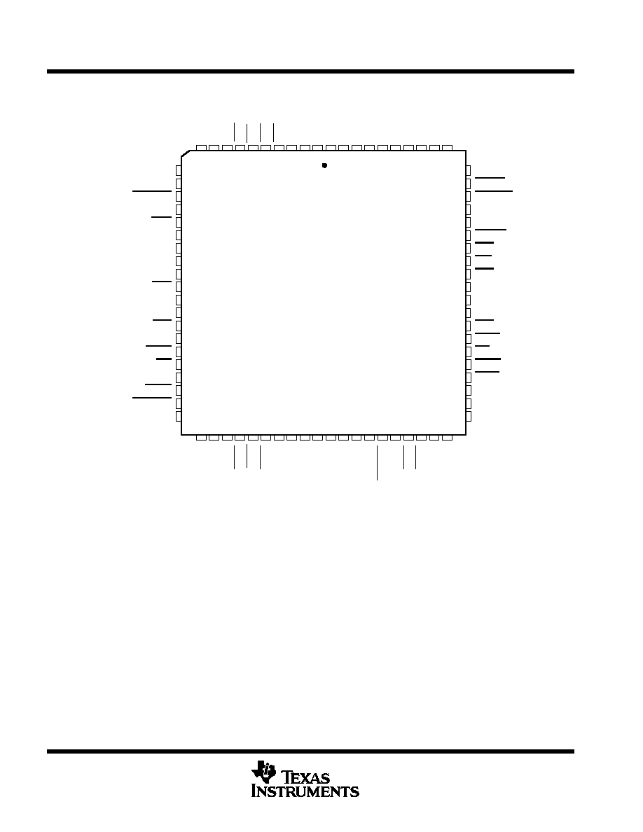
22 23
NC
ENIRQ
TXRDY1
SIN0
V
DD
RESET
CS2
IOR
IOW
A0
A1
A2
CS0
DSR0
RI0
DCD0
CTS0
GND
NC
NC
60
59
58
57
56
55
54
53
52
51
50
49
48
47
46
45
44
43
42
41
24
1
2
3
4
5
6
7
8
9
10
11
12
13
14
15
16
17
18
19
20
NC
NC
RXRDY1
SIN1
ERR
V
DD
SLCT
BUSY
PE
ACK
PEMD
TRI
CS1
CLK
DSR1
RI1
GND
DCD1
RXRDY0
NC
25 26 27 28
PN PACKAGE
(TOP VIEW)
PD2
79 78 77 76 75
80
74
INT2
SLIN
INIT
AFD
STB
GND
PD0
DB4
DB6
SOUT1
DTR1
R
TS1
CTS1
DB0
DB1
DB2
72 71 70
73
29 30 31 32 33
69 68
21
NC
PD4
67 66 65 64
34 35 36 37
DB7
TXRDY0
R
TS0
PD5
PD6
PD7
INT0
NC
INT1
DTR0
SOUT0
38 39 40
BDO
NC
63 62 61
PD1
PD3
NC
DB3
NC
DB5
NC
V
DD
description
The TL16C552A is an enhanced dual-channel version of the popular TL16C550B asynchronous
communications element (ACE). The device serves two serial input /output interfaces simultaneously in
microcomputer or microprocessor-based systems. Each channel performs serial-to-parallel conversion on data
characters received from peripheral devices or modems and parallel-to-serial conversion on data characters
transmitted by the CPU. The complete status of each channel of the dual ACE can be read at any time during
functional operation by the CPU. The information obtained includes the type and condition of the transfer
operations being performed and the error conditions encountered.
In addition to its dual communications interface capabilities, the TL16C552A provides the user with a
bidirectional parallel data port that fully supports the parallel Centronics-type printer interface. The parallel port
and the two serial ports provide IBM PC/AT-compatible computers with a single device to serve the three system
ports. A programmable baud rate generator that can divide the timing reference clock input by a divisor between
1 and (2
16
1) is included.
The TL16C552A is available in a 68-pin plastic-leaded chip-carrier (FN) package and a 80-pin TQFP (PN)
package. The TL16C552AM is available in a 68-pin ceramic quad flat (HV) package.
TL16C552A, TL16C552AM
DUAL ASYNCHRONOUS COMMUNICATIONS ELEMENT
WITH FIFO
SLLS189D NOVEMBER 1994 REVISED JANUARY 1999
3
POST OFFICE BOX 655303
·
DALLAS, TEXAS 75265
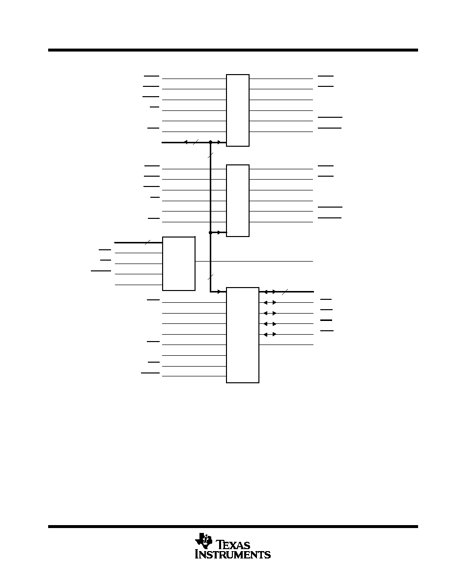
functional block diagram
CTS0
DSR0
DCD0
RI0
SIN0
CS0
DB0 DB7
RTS0
DTR0
SOUT0
INT0
RXRDY0
TXRDY0
RTS1
DTR1
SOUT1
INT1
RXRDY1
TXRDY1
BDO
24
25
26
45
9
22
12
11
10
60
61
42
53 46
57
56
55
58
59
CTS1
DSR1
DCD1
RI1
SIN1
CS1
28
31
29
30
41
32
14 21
8
8
13
5
8
6
62
3
35 33
36
37
39
4
A0 A2
IOW
IOR
RESET
CLK
ERR
SLCT
BUSY
PE
ACK
PEMD
CS2
ENIRQ
63
65
66
67
68
1
38
43
8
8
PD0 PD7
INIT
AFD
STB
SLIN
INT2
44
Select
and
Control
Logic
Parallel
Port
ACE
#2
ACE
#1
3
TL16C552A, TL16C552AM
DUAL ASYNCHRONOUS COMMUNICATIONS ELEMENT
WITH FIFO
SLLS189D NOVEMBER 1994 REVISED JANUARY 1999
4
POST OFFICE BOX 655303
·
DALLAS, TEXAS 75265
Terminal Functions
TERMINAL
NAME
NO.
I/O
DESCRIPTION
NAME
FN
PN
ACK
68
10
I
Line printer acknowledge. ACK goes low to indicate a successful data transfer has taken place. ACK
generates a printer port interrupt during its positive transition.
AFD
56
75
I/O
Line printer autofeed. AFD is an open-drain line that provides the printer with an active-low signal when
continuous form paper is to be autofed to the printer. AFD has an internal pullup resistor to VDD of
approximately 10 k
.
A0, A1, A2
35, 34,
33
51, 50,
49
I
Address. The address lines A0 A2 select the internal registers during CPU bus operations. See Table
2 for the decode of the serial channels and Table 13 for the decode of the parallel printer port.
BDO
44
63
O
Bus buffer. BDO is the active-high output and is asserted when either the serial channel or the parallel
port is read. BDO controls the system bus driver (74LS245 or 54LS245).
BUSY
66
8
I
Line printer busy. BUSY is an input line from the printer that goes high when the printer is not ready
to accept data.
CLK
4
14
I
Clock. CLK is the external clock input to the baud rate divisor of each ACE.
CS0, CS1,
CS2
32, 3,
38
48, 13,
54
I
Chip select. Each CSx input acts as an enable for the write and read signals for serial channels 1 (CS0)
and 2 (CS1). CS2 enables the signals to the printer port.
CTS0,
CTS1
28, 13
44, 26
I
Clear to send. The logical state of each CTSx terminal is reflected in the CTS bit of the modem status
register (CTS is bit 4 of the modem status register, written as MSR4) of each ACE. A change of state
in either CTS terminal since the previous reading of the associated MSR causes the setting of
CTS
(MSR0) of each modem status register.
DB0
DB7
14 21
27 34
I/O
Data bits DB0 DB7. The data bus provides eight I/O lines with 3-state outputs for the transfer of data,
control, and status information between the TL16C552A and the CPU. These lines are normally in the
high-impedance state except during read operations. DB0 is the least significant bit (LSB) and is the
first serial data bit to be received or transmitted.
DCD0,
DCD1
29, 8
45, 18
I
Data carrier detect. DCD is a modem input. Its condition can be tested by the CPU by reading MSR7
(DCD) of the modem status registers. MSR3 (
DCD) of the modem status register indicates whether
DCD has changed states since the previous reading of the MSR. DCD has no effect on the receiver.
DSR0,
DSR1
31, 5
47, 15
I
Data set ready. The logical state of the DSRx terminals is reflected in MSR5 of its associated modem
status register.
DSR (MSR1) indicates whether the associated DSRx terminal has changed states
since the previous reading of the MSR.
DTR0,
DTR1
25, 11
38, 24
O
Data terminal ready. Each DTRx can be set low by setting MCR0, modem control register bit 0 of its
associated ACE. DTRx is cleared (high) by clearing the DTR bit (MCR0) or whenever a reset occurs.
When active (low), DTRx indicates that its ACE is ready to receive data.
ENIRQ
43
59
I
Parallel port interrupt source mode selection. When ENIRQ is low, the AT mode of interrupts is enabled.
In AT mode, INT2 is internally connected to ACK. When ENIRQ is tied high, the PS-2 mode of interrupt
is enabled and INT2 is internally tied to the inverse of the PRINT bit in the line printer status register.
INT2 is latched high on the rising edge of ACK. INT2 is held until the status register is read, which then
clears the PRINT status bit and INT2.
ERR
63
5
I
Line printer error. ERR is an input line from the printer. The printer reports an error by holding ERR low
during the error condition.
GND
7, 27,
54
17, 43,
73
Ground (0 V). All terminals must be tied to GND for proper operation.
INIT
57
76
I/O
Line printer initialize. INIT is an open-drain line that provides the printer with an active-low signal that
allows the printer initialization routine to be started. INIT has an internal pullup resistor to VDD of
approximately 10 k
.
INT0, INT1
45, 60
64, 79
O
External serial channel interrupt. Each serial channel interrupt 3-state output (enabled by bit 3 of the
MCR) goes active (high) when one of the following interrupts has an active (high) condition and is
enabled by the interrupt enable register of its associated channel: receiver error flag, received data
available, transmitter holding register empty, and modem status. The interrupt is cleared on appropriate
service. Upon reset, the interrupt output is in the high-impedance state.
TL16C552A, TL16C552AM
DUAL ASYNCHRONOUS COMMUNICATIONS ELEMENT
WITH FIFO
SLLS189D NOVEMBER 1994 REVISED JANUARY 1999
5
POST OFFICE BOX 655303
·
DALLAS, TEXAS 75265
Terminal Functions (Continued)
TERMINAL
NAME
NO.
I/O
DESCRIPTION
NAME
FN
PN
INT2
59
78
O
Printer port interrupt. INT2 is an active-high, 3-state output generated by the positive transition of
ACK. INT2 is enabled by bit 4 of the write control register. Upon reset, INT2 is in the high-impedance
state. Its mode is also controlled by ENIRQ.
IOR
37
53
I
Input /output read strobe. IOR is an active-low input that enables the selected channel to output data
to the data bus (DB0 DB7). The data output depends on the register selected by the address inputs
A0, A1, A2, and chip select. Chip select 0 (CS0) selects ACE #1, chip select 1 (CS1) selects ACE #2,
and chip select 2 (CS2) selects the printer port.
IOW
36
52
I
Input/output write strobe. IOW is an active-low input causing data from the data bus to be input to either
ACE or to the parallel port. The destination depends on the register selected by the address inputs A0,
A1, A2, and chip selects CS0, CS1, and CS2.
PD0 PD7
53 46
7265
I/O
Parallel data bits (0 7). PD0 PD7 provide a byte wide input or output port to the system.
PE
67
9
I
Line printer paper empty. PE is an input line from the printer that goes high when the printer runs out
of paper.
PEMD
1
11
I
Printer enhancement mode. When low, PEMD enables the write data register to the PD0 PD7 lines.
A high on PEMD allows direction control of the PD0 PD7 port by the DIR bit in the control register.
PEMD is usually tied low for the printer operation.
RESET
39
55
I
Reset. When low, RESET forces the TL16C552A into an idle mode in which all serial data activities
are suspended. The modem control register and its associated outputs are cleared. The line status
register is cleared except for the transmitter holding register empty (THRE) and TEMT bits, which are
set. All functions of the device remain in an idle state until programmed to resume serial data activities.
RESET has a hysteresis level of typically 400 mV.
RTS0,
RTS1
24, 12
37, 25
O
Request to send. The RTS outputs are set low by setting MCR1 of its UARTs modem control register.
Both RTS terminals are reset high by RESET. A low on RTS indicates that its ACE has data ready to
transmit. In half-duplex operations, RTS controls the direction of the line.
RXRDY0,
RXRDY1
9, 61
19, 3
O
Receiver ready. Receiver direct memory access (DMA) signaling is also available through this output.
One of two types of DMA signaling can be selected using FCR3 when in FIFO mode. Only DMA mode
0 is allowed when in TL16C450 mode. For signal transfer DMA (a transfer is made between CPU bus
cycles), mode 0 is used. Multiple transfers that are made continuously until the receiver FIFO has been
emptied are supported by mode 1.
Mode 0. RXRDY is active (low) in FIFO mode (FCR0 = 1, FCR3 = 0) or in TL16C450 mode (FCR0 =
0) and the receiver FIFO or receiver holding register contains at least one character. When there are
no more characters in the FIFO or holding register, RXRDY goes inactive (high).
Mode 1. RXRDY goes active (low) in the FIFO mode (FCR0 = 1) when FCR3 = 1 and the time-out or
trigger levels have been reached. RXRDY goes inactive (high) when the FIFO or holding register is
empty.
RI0, RI1
30, 6
46, 16
I
Ring indicator. The RI signal is a modem control input. Its condition is tested by reading MSR6 (RI) of
each ACE. The modem status register output TERI (MSR2) indicates whether RI has changed from
high to low since the previous reading of the modem status register.
SIN0,
SIN1
41, 62
57, 4
I
Serial data. SIN0 and SIN1 move information from the communication line or modem to the
TL16C552A receiver circuits. Mark is a high state and space is a low state. Data on serial data inputs
is disabled in loop mode.
SLCT
65
7
I
Line printer select. SLCT is an input line from the printer that goes high when the printer is selected.
SLIN
58
77
I/O
Line printer select. SLIN is an open-drain I/O that selects the printer when active (low). SLIN has an
internal pullup resistor to VDD of approximately 10 k
.