SN54LVC574A, SN74LVC574A
OCTAL EDGE TRIGGERED D TYPE FLIP FLOPS
WITH 3 STATE OUTPUTS
SCAS301Q - JANUARY 1993 - REVISED AUGUST 2003
1
POST OFFICE BOX 655303
∑
DALLAS, TEXAS 75265
D
Operate From 1.65 V to 3.6 V
D
Inputs Accept Voltages to 5.5 V
D
Max t
pd
of 7 ns at 3.3 V
D
Typical V
OLP
(Output Ground Bounce)
<0.8 V at V
CC
= 3.3 V, T
A
= 25
∞
C
D
Typical V
OHV
(Output V
OH
Undershoot)
>2 V at V
CC
= 3.3 V, T
A
= 25
∞
C
D
Support Mixed-Mode Signal Operation on
All Ports (5-V Input/Output Voltage With
3.3-V V
CC
)
D
I
off
Supports Partial-Power-Down Mode
Operation
D
Latch-Up Performance Exceeds 250 mA Per
JESD 17
D
ESD Protection Exceeds JESD 22
- 2000-V Human-Body Model (A114-A)
- 200-V Machine Model (A115-A)
- 1000-V Charged-Device Model (C101)
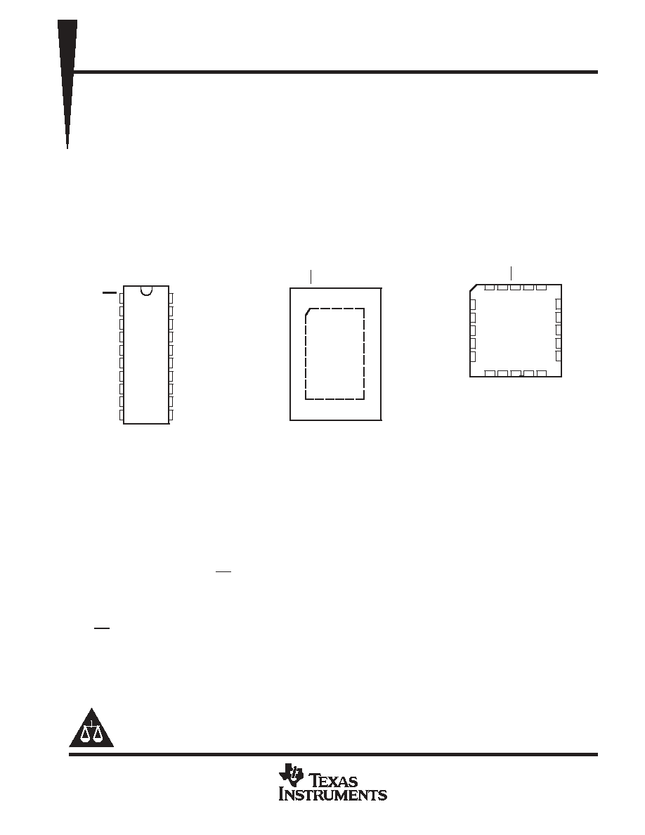
SN54LVC574A . . . J OR W PACKAGE
SN74LVC574A . . . DB, DGV, DW, N, NS,
OR PW PACKAGE
(TOP VIEW)
SN54LVC574A . . . FK PACKAGE
(TOP VIEW)
1
2
3
4
5
6
7
8
9
10
20
19
18
17
16
15
14
13
12
11
OE
1D
2D
3D
4D
5D
6D
7D
8D
GND
V
CC
1Q
2Q
3Q
4Q
5Q
6Q
7Q
8Q
CLK
3
2 1 20 19
9 10 11 12 13
4
5
6
7
8
18
17
16
15
14
2Q
3Q
4Q
5Q
6Q
3D
4D
5D
6D
7D
2D
1D
OE
8Q
7Q
1Q
8D
GND
CLK
V
CC
SN74LVC574A . . . RGY PACKAGE
(TOP VIEW)
1
20
10
11
2
3
4
5
6
7
8
9
19
18
17
16
15
14
13
12
1Q
2Q
3Q
4Q
5Q
6Q
7Q
8Q
1D
2D
3D
4D
5D
6D
7D
8D
OE
CLK
V
GND
CC
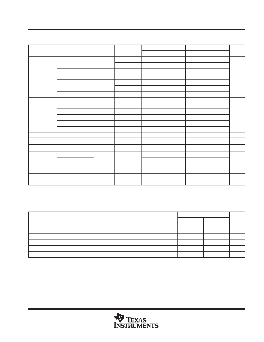
description/ordering information
The SN54LVC574A octal edge-triggered D-type flip-flop is designed for 2.7-V to 3.6-V V
CC
operation, and the
SN74LVC574A octal edge-triggered D-type flip-flop is designed for 1.65-V to 3.6-V V
CC
operation.
These devices feature 3-state outputs designed specifically for driving highly capacitive or relatively
low-impedance loads. They are particularly suitable for implementing buffer registers, I/O ports, bidirectional
bus drivers, and working registers.
On the positive transition of the clock (CLK) input, the Q outputs are set to the logic levels at the data (D) inputs.
A buffered output-enable (OE) input can be used to place the eight outputs in either a normal logic state (high
or low logic levels) or the high-impedance state. In the high-impedance state, the outputs neither load nor drive
the bus lines significantly. The high-impedance state and increased drive provide the capability to drive bus
lines without interface or pullup components.
OE does not affect the internal operations of the flip-flops. Old data can be retained or new data can be entered
while the outputs are in the high-impedance state.
These devices are fully specified for partial-power-down applications using I
off
. The I
off
circuitry disables the
outputs, preventing damaging current backflow through the device when it is powered down.
Copyright
2003, Texas Instruments Incorporated
PRODUCTION DATA information is current as of publication date.
Products conform to specifications per the terms of Texas Instruments
standard warranty. Production processing does not necessarily include
testing of all parameters.
Please be aware that an important notice concerning availability, standard warranty, and use in critical applications of
Texas Instruments semiconductor products and disclaimers thereto appears at the end of this data sheet.
On products compliant to MIL PRF 38535, all parameters are tested
unless otherwise noted. On all other products, production
processing does not necessarily include testing of all parameters.
SN54LVC574A, SN74LVC574A
OCTAL EDGE TRIGGERED D TYPE FLIP FLOPS
WITH 3 STATE OUTPUTS
SCAS301Q - JANUARY 1993 - REVISED AUGUST 2003
2
POST OFFICE BOX 655303
∑
DALLAS, TEXAS 75265
description/ordering information (continued)
To ensure the high-impedance state during power up or power down, OE should be tied to V
CC
through a pullup
resistor; the minimum value of the resistor is determined by the current-sinking capability of the driver.
Inputs can be driven from either 3.3-V or 5-V devices. This feature allows the use of these devices as translators
in a mixed 3.3-V/5-V system environment.
ORDERING INFORMATION
TA
PACKAGE
ORDERABLE
PART NUMBER
TOP-SIDE
MARKING
PDIP - N
Tube of 20
SN74LVC574AN
SN74LVC574AN
QFN - RGY
Reel of 1000
SN74LVC574ARGYR
LC574A
SOIC - DW
Tube of 25
SN74LVC574ADW
LVC574A
SOIC - DW
Reel of 2000
SN74LVC574ADWR
LVC574A
SOP - NS
Reel of 2000
SN74LVC574ANSR
LVC574A
-40
∞
C to 85
∞
C
SSOP - DB
Reel of 2000
SN74LVC574ADBR
LC574A
-40
∞
C to 85
∞
C
Tube of 70
SN74LVC574APW
TSSOP - PW
Reel of 2000
SN74LVC574APWR
LC574A
TSSOP - PW
Reel of 250
SN74LVC574APWT
LC574A
TVSOP - DGV
Reel of 2000
SN74LVC574ADGVR
LC574A
VFBGA - GQN
Reel of 1000
SN74LVC574AGQNR
LC574A
VFBGA - ZQN (Pb-free)
Reel of 1000
SN74LVC574AZQNR
LC574A
CDIP - J
Tube of 20
SNJ54LVC574AJ
SNJ54LVC574AJ
-55
∞
C to 125
∞
C
CFP - W
Tube of 85
SNJ54LVC574AW
SNJ54LVC574AW
-55 C to 125 C
LCCC - FK
Tube of 55
SNJ54LVC574AFK
SNJ54LVC574AFK
Package drawings, standard packing quantities, thermal data, symbolization, and PCB design guidelines are
available at www.ti.com/sc/package.
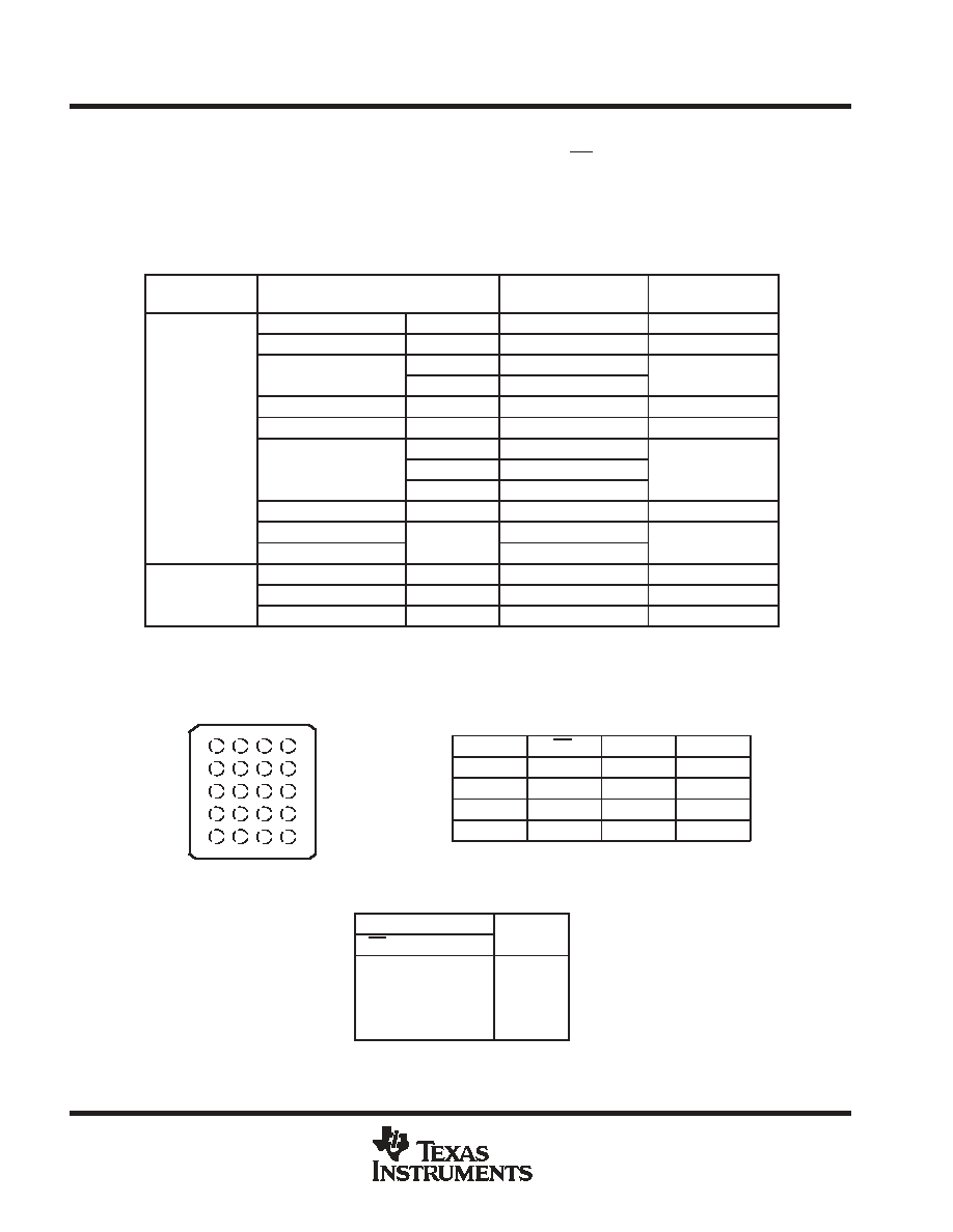
terminal assignments
1
2
3
4
A
1D
OE
VCC
1Q
B
3D
3Q
2D
2Q
C
5D
4D
5Q
4Q
D
7D
7Q
6D
6Q
E
GND
8D
CLK
8Q
FUNCTION TABLE
(each flip-flop)
INPUTS
OUTPUT
OE
CLK
D
OUTPUT
Q
L
H
H
L
L
L
L
L
X
Q0
H
X
X
Z
GQN OR ZQN PACKAGE
(TOP VIEW)
1
2
3
4
A
B
C
D
E
SN54LVC574A, SN74LVC574A
OCTAL EDGE TRIGGERED D TYPE FLIP FLOPS
WITH 3 STATE OUTPUTS
SCAS301Q - JANUARY 1993 - REVISED AUGUST 2003
3
POST OFFICE BOX 655303
∑
DALLAS, TEXAS 75265
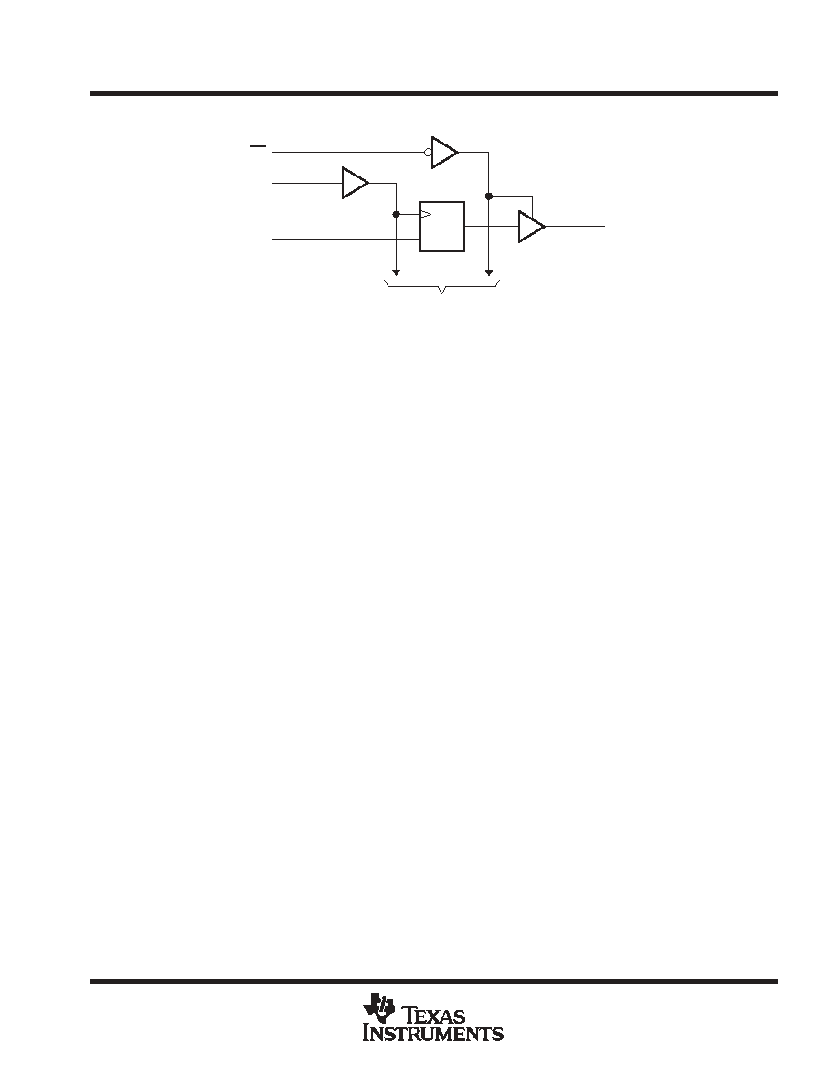
logic diagram (positive logic)
OE
CLK
1D
1Q
To Seven Other Channels
C1
1
11
2
19
1D
Pin numbers shown are for the DB, DGV, DW, FK, J, N, NS, PW, RGY, and W packages.
absolute maximum ratings over operating free-air temperature range (unless otherwise noted)
Supply voltage range, V
CC
-0.5 V to 6.5 V
. . . . . . . . . . . . . . . . . . . . . . . . . . . . . . . . . . . . . . . . . . . . . . . . . . . . . . . . .
Input voltage range, V
I
(see Note 1)
-0.5 V to 6.5 V
. . . . . . . . . . . . . . . . . . . . . . . . . . . . . . . . . . . . . . . . . . . . . . . . .
Voltage range applied to any output in the high-impedance or power-off state, V
O
(see Note 1)
-0.5 V to 6.5 V
. . . . . . . . . . . . . . . . . . . . . . . . . . . . . . . . . . . . . . . . . . . . . . . . . . . . . . . . . . . . . . . . . . .
Voltage range applied to any output in the high or low state, V
O
(see Notes 1 and 2)
-0.5 V to V
CC
+ 0.5 V
. . . . . . . . . . . . . . . . . . . . . . . . . . . . . . . . . . . . . . . . . . . . . . . . . . . . . . .
Input clamp current, I
IK
(V
I
< 0)
-50 mA
. . . . . . . . . . . . . . . . . . . . . . . . . . . . . . . . . . . . . . . . . . . . . . . . . . . . . . . . . . .
Output clamp current, I
OK
(V
O
< 0)
-50 mA
. . . . . . . . . . . . . . . . . . . . . . . . . . . . . . . . . . . . . . . . . . . . . . . . . . . . . . . .
Continuous output current, I
O
±
50 mA
. . . . . . . . . . . . . . . . . . . . . . . . . . . . . . . . . . . . . . . . . . . . . . . . . . . . . . . . . . . . .
Continuous current through V
CC
or GND
±
100 mA
. . . . . . . . . . . . . . . . . . . . . . . . . . . . . . . . . . . . . . . . . . . . . . . . . .
Package thermal impedance,
JA
(see Note 3): DB package
70
∞
C/W
. . . . . . . . . . . . . . . . . . . . . . . . . . . . . . . . .
(see Note 3): DGV package
92
∞
C/W
. . . . . . . . . . . . . . . . . . . . . . . . . . . . . . . .
(see Note 3): DW package
58
∞
C/W
. . . . . . . . . . . . . . . . . . . . . . . . . . . . . . . . .
(see Note 3): GQN/ZQN package
78
∞
C/W
. . . . . . . . . . . . . . . . . . . . . . . . . . .
(see Note 3): N package
69
∞
C/W
. . . . . . . . . . . . . . . . . . . . . . . . . . . . . . . . . . .
(see Note 3): NS package
60
∞
C/W
. . . . . . . . . . . . . . . . . . . . . . . . . . . . . . . . .
(see Note 3): PW package
83
∞
C/W
. . . . . . . . . . . . . . . . . . . . . . . . . . . . . . . . .
(see Note 4): RGY package
37
∞
C/W
. . . . . . . . . . . . . . . . . . . . . . . . . . . . . . . .
Storage temperature range, T
stg
-65
∞
C to 150
∞
C
. . . . . . . . . . . . . . . . . . . . . . . . . . . . . . . . . . . . . . . . . . . . . . . . . . .
Stresses beyond those listed under "absolute maximum ratings" may cause permanent damage to the device. These are stress ratings only, and
functional operation of the device at these or any other conditions beyond those indicated under "recommended operating conditions" is not
implied. Exposure to absolute-maximum-rated conditions for extended periods may affect device reliability.
NOTES:
1. The input negative-voltage and output voltage ratings may be exceeded if the input and output current ratings are observed.
2. The value of VCC is provided in the recommended operating conditions table.
3. The package thermal impedance is calculated in accordance with JESD 51-7.
4. The package thermal impedance is calculated in accordance with JESD 51-5.
SN54LVC574A, SN74LVC574A
OCTAL EDGE TRIGGERED D TYPE FLIP FLOPS
WITH 3 STATE OUTPUTS
SCAS301Q - JANUARY 1993 - REVISED AUGUST 2003
4
POST OFFICE BOX 655303
∑
DALLAS, TEXAS 75265
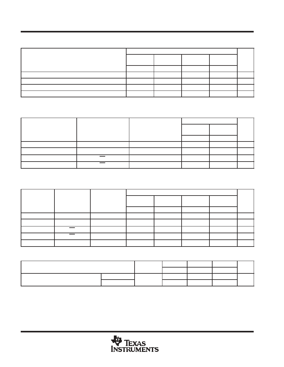
recommended operating conditions (see Note 5)
SN54LVC574A
SN74LVC574A
UNIT
MIN
MAX
MIN
MAX
UNIT
VCC
Supply voltage
Operating
2
3.6
1.65
3.6
V
VCC
Supply voltage
Data retention only
1.5
1.5
V
VCC = 1.65 V to 1.95 V
0.65
◊
VCC
VIH
High-level input voltage
VCC = 2.3 V to 2.7 V
1.7
V
VIH
High-level input voltage
VCC = 2.7 V to 3.6 V
2
2
V
VCC = 1.65 V to 1.95 V
0.35
◊
VCC
VIL
Low-level input voltage
VCC = 2.3 V to 2.7 V
0.7
V
VIL
Low-level input voltage
VCC = 2.7 V to 3.6 V
0.8
0.8
V
VI
Input voltage
0
5.5
0
5.5
V
VO
Output voltage
High or low state
0
VCC
0
VCC
V
VO
Output voltage
3-state
0
5.5
0
5.5
V
VCC = 1.65 V
-4
IOH
High-level output current
VCC = 2.3 V
-8
mA
IOH
High-level output current
VCC = 2.7 V
-12
-12
mA
VCC = 3 V
-24
-24
VCC = 1.65 V
4
IOL
Low-level output current
VCC = 2.3 V
8
mA
IOL
Low-level output current
VCC = 2.7 V
12
12
mA
VCC = 3 V
24
24
t/
v
Input transition rise or fall rate
6
6
ns/V
TA
Operating free-air temperature
-55
125
-40
85
∞
C
NOTE 5: All unused inputs of the device must be held at VCC or GND to ensure proper device operation. Refer to the TI application report,
Implications of Slow or Floating CMOS Inputs, literature number SCBA004.
SN54LVC574A, SN74LVC574A
OCTAL EDGE TRIGGERED D TYPE FLIP FLOPS
WITH 3 STATE OUTPUTS
SCAS301Q - JANUARY 1993 - REVISED AUGUST 2003
5
POST OFFICE BOX 655303
∑
DALLAS, TEXAS 75265
electrical characteristics over recommended operating free-air temperature range (unless
otherwise noted)
PARAMETER
TEST CONDITIONS
VCC
SN54LVC574A
SN74LVC574A
UNIT
PARAMETER
TEST CONDITIONS
VCC
MIN
TYP
MAX
MIN
TYP
MAX
UNIT
IOH = -100 A
1.65 V to 3.6 V
VCC-0.2
IOH = -100
µ
A
2.7 V to 3.6 V
VCC-0.2
IOH = -4 mA
1.65 V
1.2
VOH
IOH = -8 mA
2.3 V
1.7
V
VOH
IOH = -12 mA
2.7 V
2.2
2.2
V
IOH = -12 mA
3 V
2.4
2.4
IOH = -24 mA
3 V
2.2
2.2
IOL = 100 A
1.65 V to 3.6 V
0.2
IOL = 100
µ
A
2.7 V to 3.6 V
0.2
VOL
IOL = 4 mA
1.65 V
0.45
V
VOL
IOL = 8 mA
2.3 V
0.7
V
IOL = 12 mA
2.7 V
0.4
0.4
IOL = 24 mA
3 V
0.55
0.55
II
VI = 0 to 5.5 V
3.6 V
±
5
±
5
µ
A
Ioff
VI or VO = 5.5 V
0
±
10
µ
A
IOZ
VO = 0 to 5.5 V
3.6 V
±
15
±
10
µ
A
ICC
VI = VCC or GND
IO = 0
3.6 V
10
10
A
ICC
3.6 V
VI
5.5 V
IO = 0
3.6 V
10
10
µ
A
ICC
One input at VCC - 0.6 V,
Other inputs at VCC or GND
2.7 V to 3.6 V
500
500
µ
A
Ci
VI = VCC or GND
3.3 V
4
4
pF
Co
VO = VCC or GND
3.3 V
5.5
5.5
pF
All typical values are at VCC = 3.3 V, TA = 25
∞
C.
This applies in the disabled state only.
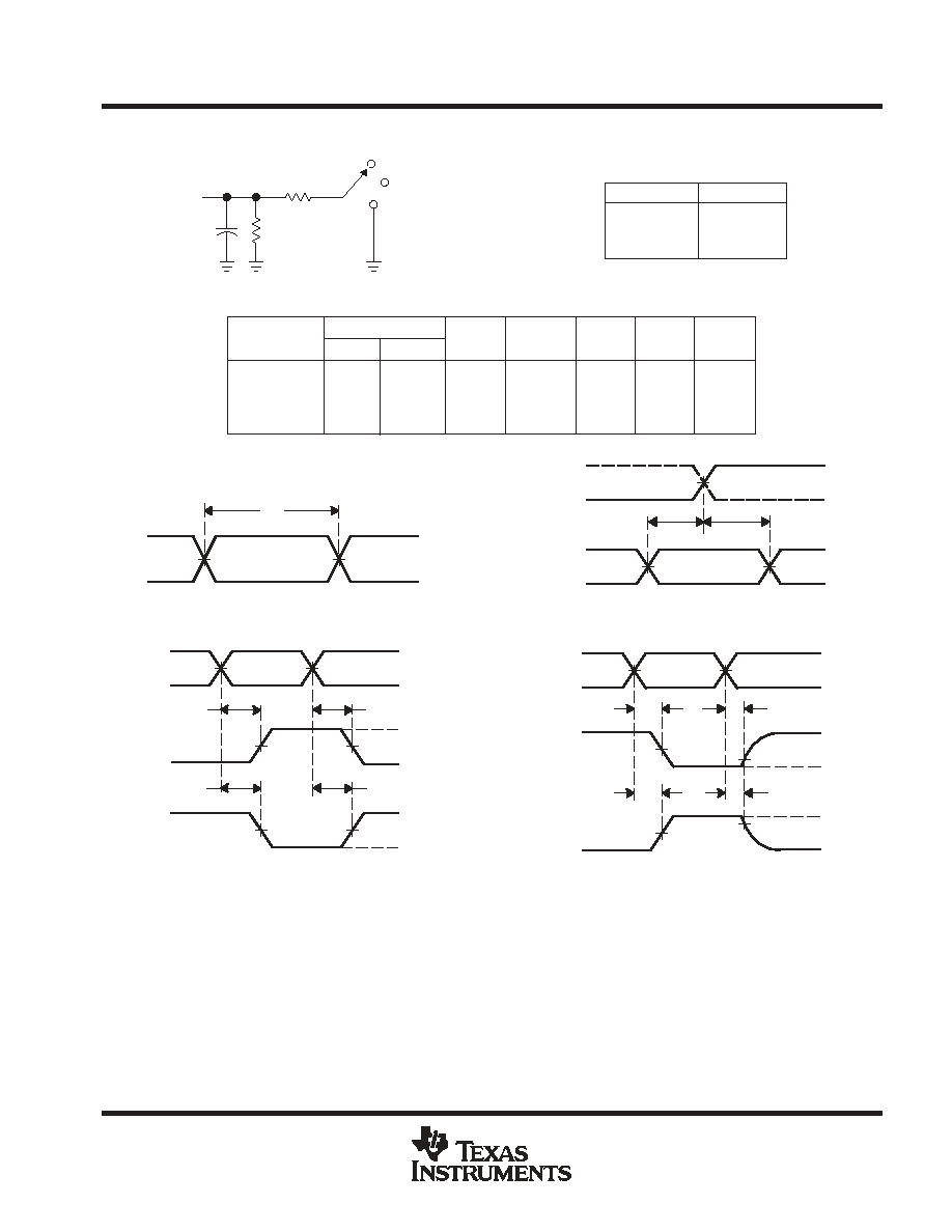
timing requirements over recommended operating free-air temperature range (unless otherwise
noted) (see Figure 1)
SN54LVC574A
VCC = 2.7 V
VCC = 3.3 V
±
0.3 V
UNIT
MIN
MAX
MIN
MAX
fclock
Clock frequency
150
150
MHz
tw
Pulse duration, CLK high or low
3.3
3.3
ns
tsu
Setup time, data before CLK
2
2
ns
th
Hold time, data after CLK
2
2
ns
SN54LVC574A, SN74LVC574A
OCTAL EDGE TRIGGERED D TYPE FLIP FLOPS
WITH 3 STATE OUTPUTS
SCAS301Q - JANUARY 1993 - REVISED AUGUST 2003
6
POST OFFICE BOX 655303
∑
DALLAS, TEXAS 75265
timing requirements over recommended operating free-air temperature range (unless otherwise
noted) (see Figure 1)
SN74LVC574A
VCC = 1.8 V
±
0.15 V
VCC = 2.5 V
±
0.2 V
VCC = 2.7 V
VCC = 3.3 V
±
0.3 V
UNIT
MIN
MAX
MIN
MAX
MIN
MAX
MIN
MAX
fclock
Clock frequency
55
95
150
150
MHz
tw
Pulse duration, CLK high or low
9
4
3.3
3.3
ns
tsu
Setup time, data before CLK
6
4
2
2
ns
th
Hold time, data after CLK
4
2
1.5
1.5
ns
switching characteristics over recommended operating free-air temperature range (unless
otherwise noted) (see Figure 1)
SN54LVC574A
PARAMETER
FROM
(INPUT)
TO
(OUTPUT)
VCC = 2.7 V
VCC = 3.3 V
±
0.3 V
UNIT
(INPUT)
(OUTPUT)
MIN
MAX
MIN
MAX
fmax
150
150
MHz
tpd
CLK
Q
8
1
7
ns
ten
OE
Q
9
1
7.5
ns
tdis
OE
Q
7
0.5
6.4
ns
switching characteristics over recommended operating free-air temperature range (unless
otherwise noted) (see Figure 1)
SN74LVC574A
PARAMETER
FROM
(INPUT)
TO
(OUTPUT)
VCC = 1.8 V
±
0.15 V
VCC = 2.5 V
±
0.2 V
VCC = 2.7 V
VCC = 3.3 V
±
0.3 V
UNIT
(INPUT)
(OUTPUT)
MIN
MAX
MIN
MAX
MIN
MAX
MIN
MAX
fmax
55
95
150
150
MHz
tpd
CLK
Q
1
21.6
1
10.5
1
8
2.2
7
ns
ten
OE
Q
1
19.5
1
10.5
1
8.5
1.5
7.5
ns
tdis
OE
Q
1
18.8
1
7.8
1
7
1.7
6.4
ns
tsk(o)
1
ns
operating characteristics, T
A
= 25
∞
C
PARAMETER
TEST
VCC = 1.8 V VCC = 2.5 V VCC = 3.3 V
UNIT
PARAMETER
TEST
CONDITIONS
TYP
TYP
TYP
UNIT
Cpd
Power dissipation capacitance
Outputs enabled
f = 10 MHz
67
60
43
pF
Cpd
Power dissipation capacitance
per flip-flop
Outputs disabled
f = 10 MHz
9
9
15
pF
SN54LVC574A, SN74LVC574A
OCTAL EDGE TRIGGERED D TYPE FLIP FLOPS
WITH 3 STATE OUTPUTS
SCAS301Q - JANUARY 1993 - REVISED AUGUST 2003
7
POST OFFICE BOX 655303
∑
DALLAS, TEXAS 75265
PARAMETER MEASUREMENT INFORMATION
VM
th
tsu
From Output
Under Test
CL
(see Note A)
LOAD CIRCUIT
S1
VLOAD
Open
GND
RL
RL
Data Input
Timing Input
VI
0 V
VI
0 V
0 V
tw
Input
VOLTAGE WAVEFORMS
SETUP AND HOLD TIMES
VOLTAGE WAVEFORMS
PROPAGATION DELAY TIMES
INVERTING AND NONINVERTING OUTPUTS
VOLTAGE WAVEFORMS
PULSE DURATION
tPLH
tPHL
tPHL
tPLH
VOH
VOH
VOL
VOL
VI
0 V
Input
Output
Waveform 1
S1 at VLOAD
(see Note B)
Output
Waveform 2
S1 at GND
(see Note B)
VOL
VOH
tPZL
tPZH
tPLZ
tPHZ
VLOAD/2
0 V
VOL + V
VOH - V
0 V
VI
VOLTAGE WAVEFORMS
ENABLE AND DISABLE TIMES
LOW- AND HIGH-LEVEL ENABLING
Output
Output
tPLH/tPHL
tPLZ/tPZL
tPHZ/tPZH
Open
VLOAD
GND
TEST
S1
NOTES: A. CL includes probe and jig capacitance.
B. Waveform 1 is for an output with internal conditions such that the output is low except when disabled by the output control.
Waveform 2 is for an output with internal conditions such that the output is high except when disabled by the output control.
C. All input pulses are supplied by generators having the following characteristics: PRR
10 MHz, ZO = 50
.
D. The outputs are measured one at a time with one transition per measurement.
E. tPLZ and tPHZ are the same as tdis.
F. tPZL and tPZH are the same as ten.
G. tPLH and tPHL are the same as tpd.
H. All parameters and waveforms are not applicable to all devices.
Output
Control
VM
VM
VM
VM
VM
VM
VM
VM
VM
VM
VM
VM
VI
VM
VM
1.8 V
±
0.15 V
2.5 V
±
0.2 V
2.7 V
3.3 V
±
0.3 V
1 k
500
500
500
VCC
RL
2
◊
VCC
2
◊
VCC
6 V
6 V
VLOAD
CL
30 pF
30 pF
50 pF
50 pF
0.15 V
0.15 V
0.3 V
0.3 V
V
VCC
VCC
2.7 V
2.7 V
VI
VCC/2
VCC/2
1.5 V
1.5 V
VM
tr/tf
2 ns
2 ns
2.5 ns
2.5 ns
INPUTS
Figure 1. Load Circuit and Voltage Waveforms

MECHANICAL DATA
MCFP004A≠ JANUARY 1995 ≠ REVISED FEBRUARY 2002
POST OFFICE BOX 655303
∑
DALLAS, TEXAS 75265
W (R-GDFP-F16)
CERAMIC DUAL FLATPACK
0.360 (9,14)
0.250 (6,35)
9
8
16
1
0.245 (6,22)
0.004 (0,10)
0.026 (0,66)
4 Places
0.015 (0,38)
0.055 (1,40)
0.370 (9,40)
0.006 (0,15)
0.045 (1,14)
Base and Seating Plane
0.005 (0,13) MIN
0.019 (0,48)
0.430 (10,92)
0.285 (7,24)
0.080 (2,03)
4040180-3 / C 02/02
0.305 (7,75) MAX
0.050 (1,27)
0.360 (9,14)
0.250 (6,35)
NOTES: A. All linear dimensions are in inches (millimeters).
B. This drawing is subject to change without notice.
C. This package can be hermetically sealed with a ceramic lid using glass frit.
D. Index point is provided on cap for terminal identification only.
E. Falls within MIL STD 1835 GDFP-1F16 and JEDEC MO-092AC
MECHANICAL DATA
MLCC006B ≠ OCTOBER 1996
POST OFFICE BOX 655303
∑
DALLAS, TEXAS 75265
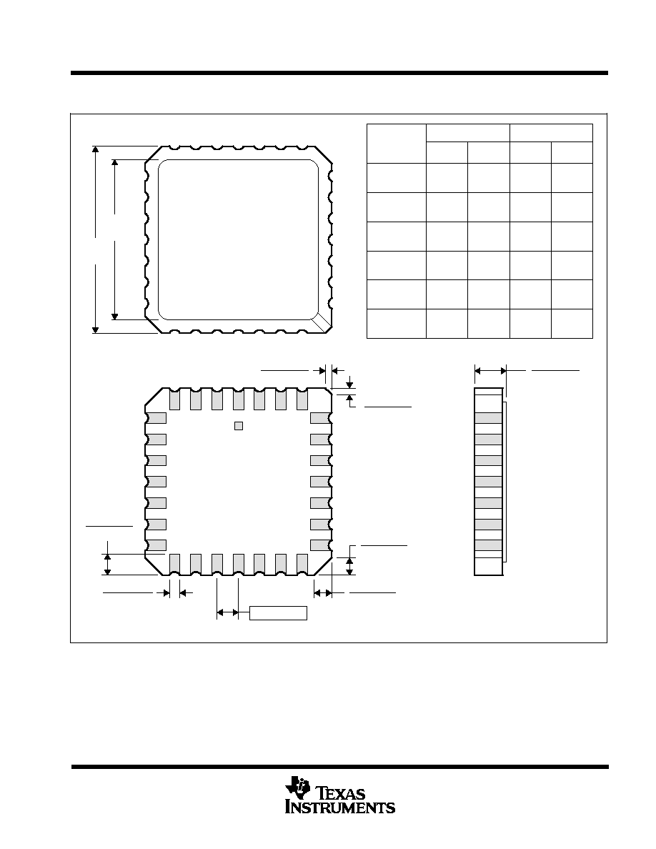
FK (S-CQCC-N**)
LEADLESS CERAMIC CHIP CARRIER
4040140 / D 10/96
28 TERMINAL SHOWN
B
0.358
(9,09)
MAX
(11,63)
0.560
(14,22)
0.560
0.458
0.858
(21,8)
1.063
(27,0)
(14,22)
A
NO. OF
MIN
MAX
0.358
0.660
0.761
0.458
0.342
(8,69)
MIN
(11,23)
(16,26)
0.640
0.739
0.442
(9,09)
(11,63)
(16,76)
0.962
1.165
(23,83)
0.938
(28,99)
1.141
(24,43)
(29,59)
(19,32)
(18,78)
**
20
28
52
44
68
84
0.020 (0,51)
TERMINALS
0.080 (2,03)
0.064 (1,63)
(7,80)
0.307
(10,31)
0.406
(12,58)
0.495
(12,58)
0.495
(21,6)
0.850
(26,6)
1.047
0.045 (1,14)
0.045 (1,14)
0.035 (0,89)
0.035 (0,89)
0.010 (0,25)
12
13
14
15
16
18
17
11
10
8
9
7
5
4
3
2
0.020 (0,51)
0.010 (0,25)
6
1
28
26
27
19
21
B SQ
A SQ
22
23
24
25
20
0.055 (1,40)
0.045 (1,14)
0.028 (0,71)
0.022 (0,54)
0.050 (1,27)
NOTES: A. All linear dimensions are in inches (millimeters).
B. This drawing is subject to change without notice.
C. This package can be hermetically sealed with a metal lid.
D. The terminals are gold plated.
E. Falls within JEDEC MS-004

MECHANICAL DATA
MPBG133C ≠ APRIL 2000 ≠ REVISED AUGUST 2002
POST OFFICE BOX 655303
∑
DALLAS, TEXAS 75265
GQN (R-PBGA-N20)
PLASTIC BALL GRID ARRAY
M
0,05
0,65
0,08
4200704/D 07/2002
3,90
4,10
3,10
2,90
1,00 MAX
0,35
0,45
1
Seating Plane
1,95 TYP
A
2,60
2
3
4
B
C
D
E
0,15
0,25
0,325
0,65
A1 Corner
Bottom View
20
◊
NOTES: A. All linear dimensions are in millimeters.
B. This drawing is subject to change without notice.
C. MicroStar Junior
t
configuration
D. Falls within JEDEC MO-225 variation BC.
E. This package is tin-lead (SnPb). Refer to the 20 ZQN package (drawing 4204492) for lead-free.
MicroStar Junior is a trademark of Texas Instruments.

MECHANICAL DATA
MPBG297 ≠ JULY 2002
POST OFFICE BOX 655303
∑
DALLAS, TEXAS 75265
ZQN (R-PBGA-N20)
PLASTIC BALL GRID ARRAY
4,10
3,90
3,10
2,90
Bottom View
A
1
2
C
B
D
E
3
4
4204492/A 06/2002
20
◊
0,05
0,35
0,45
M
0,25
0,15
Seating Plane
0,08
1,00 Max
A1 Corner
2,60
0,65
0,325
1,95
0,65
NOTES: A. All linear dimensions are in millimeters.
B. This drawing is subject to change without notice.
C. MicroStar Junior
configuration.
D. Fall within JEDEC MO-225 variation BC.
E. This package is lead-free. Refer to the 20 GQN package (drawing 4200704) for tin-lead )SnPb).
MicroStar Junior is a trademark of Texas Instruments.
MECHANICAL
MPDI002C ≠ JANUARY 1995 ≠ REVISED DECEMBER 20002
POST OFFICE BOX 655303
∑
DALLAS, TEXAS 75265
N (R-PDIP-T**)
PLASTIC DUAL-IN-LINE PACKAGE
BB
AC
AD
0.325 (8,26)
0.300 (7,62)
0.010 (0,25) NOM
Gauge Plane
0.015 (0,38)
0.430 (10,92) MAX
20
1.060
(26,92)
0.940
(23,88)
18
0.920
0.850
14
0.775
0.745
(19,69)
(18,92)
16
0.775
(19,69)
(18,92)
0.745
A MIN
DIM
A MAX
PINS **
(23,37)
(21,59)
Seating Plane
14/18 PIN ONLY
20 pin vendor option
4040049/E 12/2002
9
8
0.070 (1,78)
A
0.045 (1,14)
0.020 (0,51) MIN
16
1
0.015 (0,38)
0.021 (0,53)
0.200 (5,08) MAX
0.125 (3,18) MIN
0.240 (6,10)
0.260 (6,60)
M
0.010 (0,25)
0.100 (2,54)
16 PINS SHOWN
MS-100
VARIATION
AA
C
D
D
D
0.030 (0,76)
0.045 (1,14)
NOTES: A. All linear dimensions are in inches (millimeters).
B. This drawing is subject to change without notice.
C. Falls within JEDEC MS-001, except 18 and 20 pin minimum body lrngth (Dim A).
D. The 20 pin end lead shoulder width is a vendor option, either half or full width.
MECHANICAL DATA
MPDS006C ≠ FEBRUARY 1996 ≠ REVISED AUGUST 2000
POST OFFICE BOX 655303
∑
DALLAS, TEXAS 75265
DGV (R-PDSO-G**)
PLASTIC SMALL-OUTLINE
24 PINS SHOWN
14
3,70
3,50
4,90
5,10
20
DIM
PINS **
4073251/E 08/00
1,20 MAX
Seating Plane
0,05
0,15
0,25
0,50
0,75
0,23
0,13
1
12
24
13
4,30
4,50
0,16 NOM
Gage Plane
A
7,90
7,70
38
24
16
4,90
5,10
3,70
3,50
A MAX
A MIN
6,60
6,20
11,20
11,40
56
9,60
9,80
48
0,08
M
0,07
0,40
0
∞
≠ 8
∞
NOTES: A. All linear dimensions are in millimeters.
B. This drawing is subject to change without notice.
C. Body dimensions do not include mold flash or protrusion, not to exceed 0,15 per side.
D. Falls within JEDEC: 24/48 Pins ≠ MO-153
14/16/20/56 Pins ≠ MO-194

MECHANICAL DATA
MSOI003E ≠ JANUARY 1995 ≠ REVISED SEPTEMBER 2001
POST OFFICE BOX 655303
∑
DALLAS, TEXAS 75265
DW (R-PDSO-G**)
PLASTIC SMALL-OUTLINE PACKAGE
16 PINS SHOWN
0.419 (10,65)
0.400 (10,15)
0.291 (7,39)
0.299 (7,59)
16
0.400
(10,16)
A MIN
A MAX
(10,41)
0.410
0.462
(11,73)
(11,51)
0.453
18
0.610
(15,49)
(15,24)
0.600
24
DIM
PINS **
4040000/E 08/01
0.104 (2,65) MAX
0.004 (0,10)
0.012 (0,30)
Seating Plane
0
∞
≠ 8
∞
0.016 (0,40)
0.050 (1,27)
16
0.050 (1,27)
1
A
8
9
0.014 (0,35)
0.020 (0,51)
0.010 (0,25) NOM
Gage Plane
0.010 (0,25)
28
0.710
(18,03)
0.700
(17,78)
(12,70)
(12,95)
0.500
20
0.510
0.010 (0,25)
0.004 (0,10)
NOTES: A. All linear dimensions are in inches (millimeters).
B. This drawing is subject to change without notice.
C. Body dimensions do not include mold flash or protrusion not to exceed 0.006 (0,15).
D. Falls within JEDEC MS-013

MECHANICAL DATA
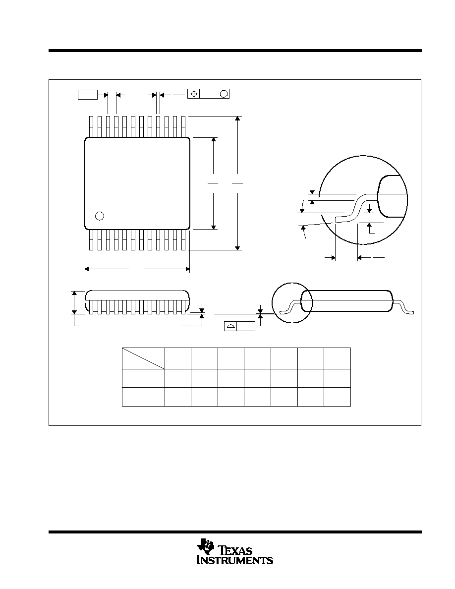
MSSO002E ≠ JANUARY 1995 ≠ REVISED DECEMBER 2001
POST OFFICE BOX 655303
∑
DALLAS, TEXAS 75265
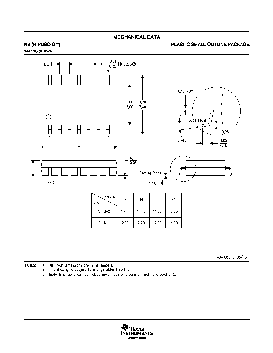
DB (R-PDSO-G**)
PLASTIC SMALL-OUTLINE
4040065 /E 12/01
28 PINS SHOWN
Gage Plane
8,20
7,40
0,55
0,95
0,25
38
12,90
12,30
28
10,50
24
8,50
Seating Plane
9,90
7,90
30
10,50
9,90
0,38
5,60
5,00
15
0,22
14
A
28
1
20
16
6,50
6,50
14
0,05 MIN
5,90
5,90
DIM
A MAX
A MIN
PINS **
2,00 MAX
6,90
7,50
0,65
M
0,15
0
∞
≠ 8
∞
0,10
0,09
0,25
NOTES: A. All linear dimensions are in millimeters.
B. This drawing is subject to change without notice.
C. Body dimensions do not include mold flash or protrusion not to exceed 0,15.
D. Falls within JEDEC MO-150
MECHANICAL DATA
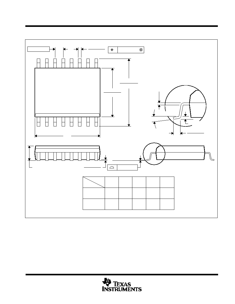
MTSS001C ≠ JANUARY 1995 ≠ REVISED FEBRUARY 1999
POST OFFICE BOX 655303
∑
DALLAS, TEXAS 75265
PW (R-PDSO-G**)
PLASTIC SMALL-OUTLINE PACKAGE
14 PINS SHOWN
0,65
M
0,10
0,10
0,25
0,50
0,75
0,15 NOM
Gage Plane
28
9,80
9,60
24
7,90
7,70
20
16
6,60
6,40
4040064/F 01/97
0,30
6,60
6,20
8
0,19
4,30
4,50
7
0,15
14
A
1
1,20 MAX
14
5,10
4,90
8
3,10
2,90
A MAX
A MIN
DIM
PINS **
0,05
4,90
5,10
Seating Plane
0
∞
≠ 8
∞
NOTES: A. All linear dimensions are in millimeters.
B. This drawing is subject to change without notice.
C. Body dimensions do not include mold flash or protrusion not to exceed 0,15.
D. Falls within JEDEC MO-153

IMPORTANT NOTICE
Texas Instruments Incorporated and its subsidiaries (TI) reserve the right to make corrections, modifications,
enhancements, improvements, and other changes to its products and services at any time and to discontinue
any product or service without notice. Customers should obtain the latest relevant information before placing
orders and should verify that such information is current and complete. All products are sold subject to TI's terms
and conditions of sale supplied at the time of order acknowledgment.
TI warrants performance of its hardware products to the specifications applicable at the time of sale in
accordance with TI's standard warranty. Testing and other quality control techniques are used to the extent TI
deems necessary to support this warranty. Except where mandated by government requirements, testing of all
parameters of each product is not necessarily performed.
TI assumes no liability for applications assistance or customer product design. Customers are responsible for
their products and applications using TI components. To minimize the risks associated with customer products
and applications, customers should provide adequate design and operating safeguards.
TI does not warrant or represent that any license, either express or implied, is granted under any TI patent right,
copyright, mask work right, or other TI intellectual property right relating to any combination, machine, or process
in which TI products or services are used. Information published by TI regarding third-party products or services
does not constitute a license from TI to use such products or services or a warranty or endorsement thereof.
Use of such information may require a license from a third party under the patents or other intellectual property
of the third party, or a license from TI under the patents or other intellectual property of TI.
Reproduction of information in TI data books or data sheets is permissible only if reproduction is without
alteration and is accompanied by all associated warranties, conditions, limitations, and notices. Reproduction
of this information with alteration is an unfair and deceptive business practice. TI is not responsible or liable for
such altered documentation.
Resale of TI products or services with statements different from or beyond the parameters stated by TI for that
product or service voids all express and any implied warranties for the associated TI product or service and
is an unfair and deceptive business practice. TI is not responsible or liable for any such statements.
Following are URLs where you can obtain information on other Texas Instruments products and application
solutions:
Products
Applications
Amplifiers
amplifier.ti.com
Audio
www.ti.com/audio
Data Converters
dataconverter.ti.com
Automotive
www.ti.com/automotive
DSP
dsp.ti.com
Broadband
www.ti.com/broadband
Interface
interface.ti.com
Digital Control
www.ti.com/digitalcontrol
Logic
logic.ti.com
Military
www.ti.com/military
Power Mgmt
power.ti.com
Optical Networking
www.ti.com/opticalnetwork
Microcontrollers
microcontroller.ti.com
Security
www.ti.com/security
Telephony
www.ti.com/telephony
Video & Imaging
www.ti.com/video
Wireless
www.ti.com/wireless
Mailing Address:
Texas Instruments
Post Office Box 655303 Dallas, Texas 75265
Copyright
2003, Texas Instruments Incorporated