SN54F153, SN74F153
DUAL 1-OF-4 DATA SELECTORS/MULTIPLEXERS
SDFS052A ≠ D2932, MARCH 1987 ≠ REVISED OCTOBER 1993
Copyright
©
1993, Texas Instruments Incorporated
2≠1
POST OFFICE BOX 655303
∑
DALLAS, TEXAS 75265
∑
Permits Multiplexing From N Lines to
One Line
∑
Performs Parallel-to-Serial Conversion
∑
Strobe (Enable) Line Provided for
Cascading (N Lines to N Lines)
∑
Package Options Include Plastic
Small-Outline Packages, Ceramic Chip
Carriers, and Standard Plastic and Ceramic
300-mil DIPs
description
These data selectors/multiplexers contain
inverters and drivers to supply full binary decoding
data selection to the AND-OR gates. Separate
strobe (G) inputs are provided for each of the two
4-line sections.
The SN54F153 is characterized for operation over
the full military temperature range of ≠ 55
∞
C to
125
∞
C. The SN74F153 is characterized for
operation from 0
∞
C to 70
∞
C.
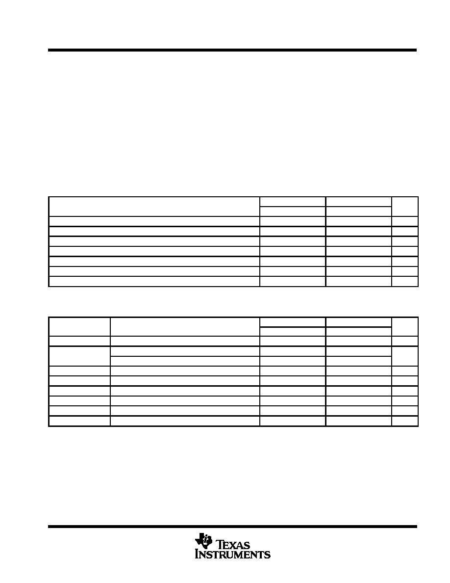
FUNCTION TABLE
INPUTS
STROBE
OUTPUT
SELECT
DATA
STROBE
G
OUTPUT
Y
B
A
C0
C1
C2
C3
G
Y
X
X
X
X
X
X
H
L
L
L
L
X
X
X
L
L
L
L
H
X
X
X
L
H
L
H
X
L
X
X
L
L
L
H
X
H
X
X
L
H
H
L
X
X
L
X
L
L
H
L
X
X
H
X
L
H
H
H
X
X
X
L
L
L
H
H
X
X
X
H
L
H
Select inputs A and B are common to both sections.
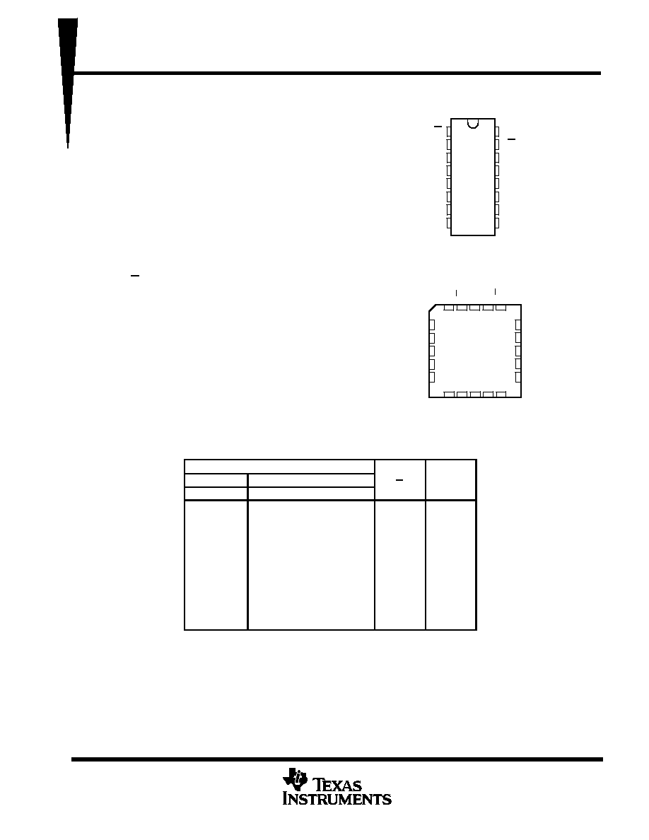
SN54F153 . . . J PACKAGE
SN74F153 . . . D OR N PACKAGE
(TOP VIEW)
3
2
1 20 19
9 10 11 12 13
4
5
6
7
8
18
17
16
15
14
A
2C3
NC
2C2
2C1
1C3
1C2
NC
1C1
1C0
SN54F153 . . . FK PACKAGE
(TOP VIEW)
B
1G
NC
2Y
2C0
2G
1Y
GND
NC
NC ≠ No internal connection
V
CC
1
2
3
4
5
6
7
8
16
15
14
13
12
11
10
9
1G
B
1C3
1C2
1C1
1C0
1Y
GND
V
CC
2G
A
2C3
2C2
2C1
2C0
2Y
PRODUCTION DATA information is current as of publication date.
Products conform to specifications per the terms of Texas Instruments
standard warranty. Production processing does not necessarily include
testing of all parameters.

SN54F153, SN74F153
DUAL 1-OF-4 DATA SELECTORS/MULTIPLEXERS
SDFS052A ≠ D2932, MARCH 1987 ≠ REVISED OCTOBER 1993
2≠2
POST OFFICE BOX 655303
∑
DALLAS, TEXAS 75265
logic symbol
G
MUX
0
3
0
14
A
1
2
B
EN
1
15
1Y
7
0
6
1C0
1
5
1C1
2
4
1C2
3
3
1C3
10
2C0
11
2C1
12
2C2
13
2C3
2Y
9
1G
2G
This symbol is in accordance with ANSI/IEEE Std 91-1984 and IEC Publication 617-12.
Pin numbers shown are for the D, J, and N packages.
SN54F153, SN74F153
DUAL 1-OF-4 DATA SELECTORS/MULTIPLEXERS
SDFS052A ≠ D2932, MARCH 1987 ≠ REVISED OCTOBER 1993
2≠3
POST OFFICE BOX 655303
∑
DALLAS, TEXAS 75265
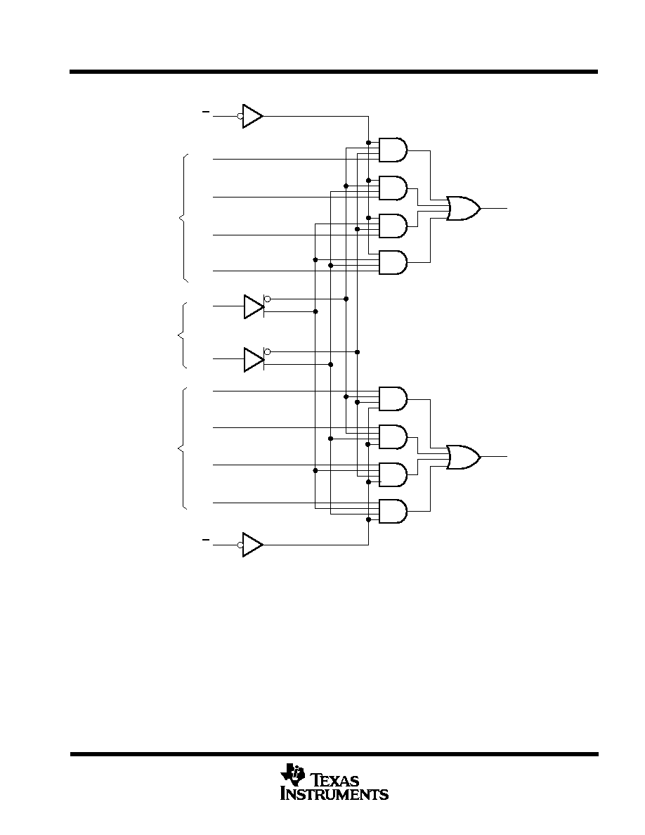
logic diagram (positive logic)
Data 2
Select
Data 1
2G
2C3
2C2
2C1
2C0
A
B
1C3
1C2
1C1
1C0
1G
2Y
1Y
1
6
5
4
3
2
14
10
11
12
13
15
7
9
Pin numbers shown are for the D, J, and N packages.
SN54F153, SN74F153
DUAL 1-OF-4 DATA SELECTORS/MULTIPLEXERS
SDFS052A ≠ D2932, MARCH 1987 ≠ REVISED OCTOBER 1993
2≠4
POST OFFICE BOX 655303
∑
DALLAS, TEXAS 75265
absolute maximum ratings over operating free-air temperature range (unless otherwise noted)
Supply voltage range, V
CC
≠ 0.5 V to 7 V
. . . . . . . . . . . . . . . . . . . . . . . . . . . . . . . . . . . . . . . . . . . . . . . . . . . . . . . . . .
Input voltage range (see Note 1)
≠ 1.2 V to 7 V
. . . . . . . . . . . . . . . . . . . . . . . . . . . . . . . . . . . . . . . . . . . . . . . . . . . . .
Input current range
≠ 30 mA to 5 mA
. . . . . . . . . . . . . . . . . . . . . . . . . . . . . . . . . . . . . . . . . . . . . . . . . . . . . . . . . . . . . .
Voltage range applied to any output in the high state
≠ 0.5 V to V
CC
. . . . . . . . . . . . . . . . . . . . . . . . . . . . . . . . . .
Current into any output in the low state
40 mA
. . . . . . . . . . . . . . . . . . . . . . . . . . . . . . . . . . . . . . . . . . . . . . . . . . . . . .
Operating free-air temperature range: SN54F153
≠ 55
∞
C to 125
∞
C
. . . . . . . . . . . . . . . . . . . . . . . . . . . . . . . . . . .
SN74F153
0
∞
C to 70
∞
C
. . . . . . . . . . . . . . . . . . . . . . . . . . . . . . . . . . . . . . .
Storage temperature range
≠ 65
∞
C to 150
∞
C
. . . . . . . . . . . . . . . . . . . . . . . . . . . . . . . . . . . . . . . . . . . . . . . . . . . . . . .
Stresses beyond those listed under "absolute maximum ratings" may cause permanent damage to the device. These are stress ratings only and
functional operation of the device at these or any other conditions beyond those indicated under "recommended operating conditions" is not
implied. Exposure to absolute-maximum-rated conditions for extended periods may affect device reliability.
NOTE 1: The input voltage rating may be exceeded provided that the input current rating is observed.
recommended operating conditions
SN54F153
SN74F153
UNIT
MIN
NOM
MAX
MIN
NOM
MAX
UNIT
VCC
Supply voltage
4.5
5
5.5
4.5
5
5.5
V
VIH
High-level input voltage
2
2
V
VIL
Low-level input voltage
0.8
0.8
V
IIK
Input clamp current
≠ 18
≠ 18
mA
IOH
High-level output current
≠ 1
≠ 1
mA
IOL
Low-level output current
20
20
mA
TA
Operating free-air temperature
≠ 55
125
0
70
∞
C
electrical characteristics over recommended operating free-air temperature range (unless
otherwise noted)
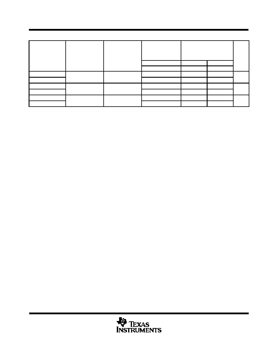
PARAMETER
TEST CONDITIONS
SN54F153
SN74F153
UNIT
PARAMETER
TEST CONDITIONS
MIN
TYP
MAX
MIN
TYP
MAX
UNIT
VIK
VCC = 4.5 V,
II = ≠ 18 mA
≠ 1.2
≠ 1.2
V
VOH
VCC = 4.5 V,
IOH = ≠ 1 mA
2.5
3.4
2.5
3.4
V
VOH
VCC = 4.75 V,
IOH = ≠ 1 mA
2.7
V
VOL
VCC = 4.5 V,
IOL = 20 mA
0.3
0.5
0.3
0.5
V
II
VCC = 5.5 V,
VI = 7 V
0.1
0.1
mA
IIH
VCC = 5.5 V,
VI = 2.7 V
20
20
µ
A
IIL
VCC = 5.5 V,
VI = 0.5 V
≠ 0.6
≠ 0.6
mA
IOSß
VCC = 5.5 V,
VO = 0
≠ 60
≠150
≠ 60
≠150
mA
ICC
VCC = 5.5 V,
VI = 0
12
20
12
20
mA
All typical values are at VCC = 5 V, TA = 25
∞
C.
ß Not more than one output should be shorted at a time, and the duration of the short circuit should not exceed one second.
SN54F153, SN74F153
DUAL 1-OF-4 DATA SELECTORS/MULTIPLEXERS
SDFS052A ≠ D2932, MARCH 1987 ≠ REVISED OCTOBER 1993
2≠5
POST OFFICE BOX 655303
∑
DALLAS, TEXAS 75265
switching characteristics (see Note 2)
PARAMETER
FROM
(INPUT)
TO
(OUTPUT)
VCC = 5 V,
CL = 50 pF,
RL = 500
,
TA = 25
∞
C
VCC = 4.5 V to 5.5 V,
CL = 50 pF,
RL = 500
,
TA = MIN to MAX
UNIT
(
)
(
)
F153
SN54F153
SN74F153
MIN
TYP
MAX
MIN
MAX
MIN
MAX
tPLH
A or B
Y
3.7
7.7
10.5
3.7
14
3.7
12
ns
tPHL
A or B
Y
2.7
6.6
9
2.7
11
2.7
10.5
ns
tPLH
G
Y
3.7
6.7
9
3.7
11.5
3.7
10.5
ns
tPHL
G
Y
2.2
5.3
7
1.7
9
1.7
8
ns
tPLH
C
Y
2.2
4.9
7
1.7
9
2.2
8
ns
tPHL
C
Y
2.2
4.7
6.5
1.7
8
1.7
7.5
ns
For conditions shown as MIN or MAX, use the appropriate value specified under recommended operating conditions.
NOTE 2: Load circuits and voltage waveforms are shown in Section 1.