www.ti.com
FEATURES
1
2
3
4
5
6
7
14
13
12
11
10
9
8
1A
1Y
2A
2Y
3A
3Y
GND
V
CC
6A
6Y
5A
5Y
4A
4Y
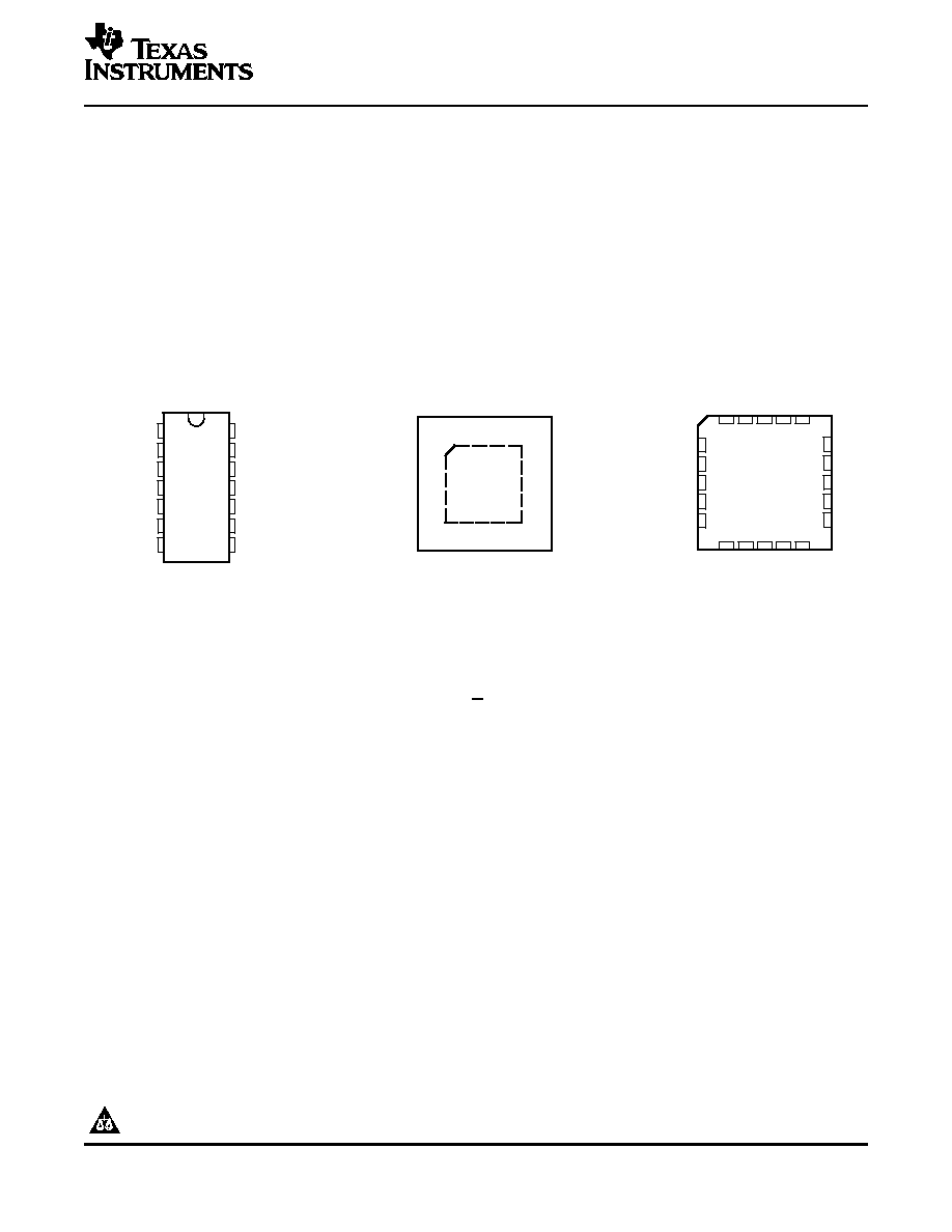
SN54LVC04A . . . J OR W PACKAGE
SN74LVC04A . . . D, DB, DGV, NS,
OR PW PACKAGE
(TOP VIEW)
3
2 1 20 19
9 10 11 12 13
4
5
6
7
8
18
17
16
15
14
6Y
NC
5A
NC
5Y
2A
NC
2Y
NC
3A
1Y
1A
NC
4Y
4A
V
6A
3Y
GND
NC
SN54LVC04A . . . FK PACKAGE
(TOP VIEW)
CC
NC - No internal connection
SN74LVC04A . . . RGY PACKAGE
(TOP VIEW)
1
14
7
8
2
3
4
5
6
13
12
11
10
9
6A
6Y
5A
5Y
4A
1Y
2A
2Y
3A
3Y
1A
4Y
V
GND
CC
DESCRIPTION/ORDERING INFORMATION
SN54LVC04A, SN74LVC04A
HEX INVERTERS
SCAS281R ≠ JANUARY 1993 ≠ REVISED JULY 2005
∑
Operate From 1.65 V to 3.6 V
∑
Latch-Up Performance Exceeds 250 mA Per
JESD 17
∑
Specified From ≠40įC to 85įC,
≠40įC to 125įC, and ≠55įC to 125įC
∑
ESD Protection Exceeds JESD 22
∑
Inputs Accept Voltages to 5.5 V
≠ 2000-V Human-Body Model (A114-A)
∑
Max t
pd
of 4.5 ns at 3.3 V
≠ 200-V Machine Model (A115-A)
∑
Typical V
OLP
(Output Ground Bounce)
≠ 1000-V Charged-Device Model (C101)
<0.8 V at V
CC
= 3.3 V, T
A
= 25įC
xxxx
xxxx
∑
Typical V
OHV
(Output V
OH
Undershoot)
xxxx
>2 V at V
CC
= 3.3 V, T
A
= 25įC
The SN54LVC04A hex inverter contains six independent inverters designed for 2.7-V to 3.6-V V
CC
operation, and
the SN74LVC04A hex inverter contains six independent inverters designed for 1.65-V to 3.6-V V
CC
operation.
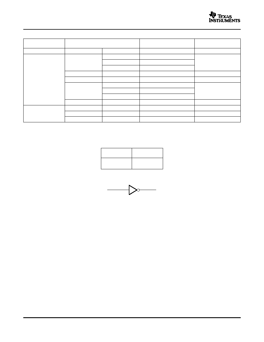
The 'LVC04A devices perform the Boolean function Y = A.
Inputs can be driven from either 3.3-V or 5-V devices. This feature allows the use of these devices as translators
in a mixed 3.3-V/5-V system environment.
Please be aware that an important notice concerning availability, standard warranty, and use in critical applications of Texas
Instruments semiconductor products and disclaimers thereto appears at the end of this data sheet.
PRODUCTION DATA information is current as of publication date.
Copyright © 1993≠2005, Texas Instruments Incorporated
Products conform to specifications per the terms of the Texas
On products compliant to MIL-PRF-38535, all parameters are
Instruments standard warranty. Production processing does not
tested unless otherwise noted. On all other products, production
necessarily include testing of all parameters.
processing does not necessarily include testing of all parameters.
www.ti.com
A
Y
SN54LVC04A, SN74LVC04A
HEX INVERTERS
SCAS281R ≠ JANUARY 1993 ≠ REVISED JULY 2005
ORDERING INFORMATION
ORDERABLE
TOP-SIDE
T
A
PACKAGE
(1)
PART NUMBER
MARKING
≠40įC to 85įC
QFN ≠ RGY
Reel of 1000
SN74LVC04ARGYR
LC04A
Tube of 50
SN74LVC04AD
SOIC ≠ D
Reel of 2500
SN74LVC04ADR
LVC04A
Reel of 250
SN74LVC04ADT
SOP ≠ NS
Reel of 2000
SN74LVC04ANSR
LVC04A
≠40įC to 125įC
SSOP - DB
Reel of 2000
SN74LVC04ADBR
LC04A
Tube of 90
SN74LVC04APW
TSSOP ≠ PW
Reel of 2000
SN74LVC04APWR
LC04A
Reel of 250
SN74LVC04APWT
TVSOP ≠ DGV
Reel of 2000
SN74LVC04ADGVR
LC04A
CDIP ≠ J
Tube of 25
SNJ54LVC04AJ
SNJ54LVC04AJ
≠55įC to 125įC
CFP ≠ W
Tube of 150
SNJ54LVC04AW
SNJ54LVC04AW
LCCC ≠ FK
Tube of 55
SNJ54LVC04AFK
SNJ54LVC04AFK
(1)
Package drawings, standard packing quantities, thermal data, symbolization, and PCB design guidelines are available at
www.ti.com/sc/package.
FUNCTION TABLE
(EACH INVERTER)
INPUT
OUTPUT
A
Y
H
L
L
H
LOGIC DIAGRAM, EACH INVERTER (POSITIVE LOGIC)
2

www.ti.com
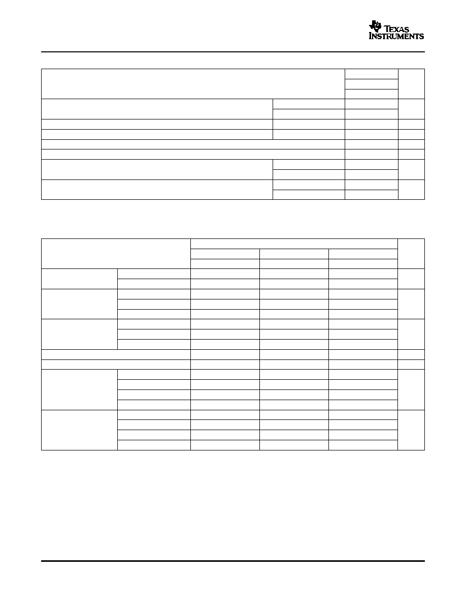
Absolute Maximum Ratings
(1)
SN54LVC04A, SN74LVC04A
HEX INVERTERS
SCAS281R ≠ JANUARY 1993 ≠ REVISED JULY 2005
over operating free-air temperature range (unless otherwise noted)
MIN
MAX
UNIT
V
CC
Supply voltage range
≠0.5
6.5
V
V
I
Input voltage range
(2)
≠0.5
6.5
V
V
O
Output voltage range
(2) (3)
≠0.5
V
CC
+ 0.5
V
I
IK
Input clamp current
V
I
< 0
≠50
mA
I
OK
Output clamp current
V
O
< 0
≠50
mA
I
O
Continuous output current
Ī50
mA
Continuous current through V
CC
or GND
Ī100
mA
D package
(4)
86
DB package
(4)
96
DGV package
(4)
127
JA
Package thermal impedance
įC/W
NS package
(4)
76
PW package
(4)
113
RGY package
(5)
47
T
stg
Storage temperature range
≠65
150
įC
P
tot
Power dissipation
T
A
= ≠40įC to 125įC
(6) (7)
500
mW
(1)
Stresses beyond those listed under "absolute maximum ratings" may cause permanent damage to the device. These are stress ratings
only, and functional operation of the device at these or any other conditions beyond those indicated under "recommended operating
conditions" is not implied. Exposure to absolute-maximum-rated conditions for extended periods may affect device reliability.
(2)
The input and output negative-voltage ratings may be exceeded if the input and output current ratings are observed.
(3)
The value of V
CC
is provided in the recommended operating conditions table.
(4)
The package thermal impedance is calculated in accordance with JESD 51-7.
(5)
The package thermal impedance is calculated in accordance with JESD 51-5.
(6)
For the D package: above 70įC, the value of P
tot
derates linearly with 8 mW/K.
(7)
For the DB, DGV, NS, and PW packages: above 60įC, the value of P
tot
derates linearly with 5.5 mW/K.
3
www.ti.com
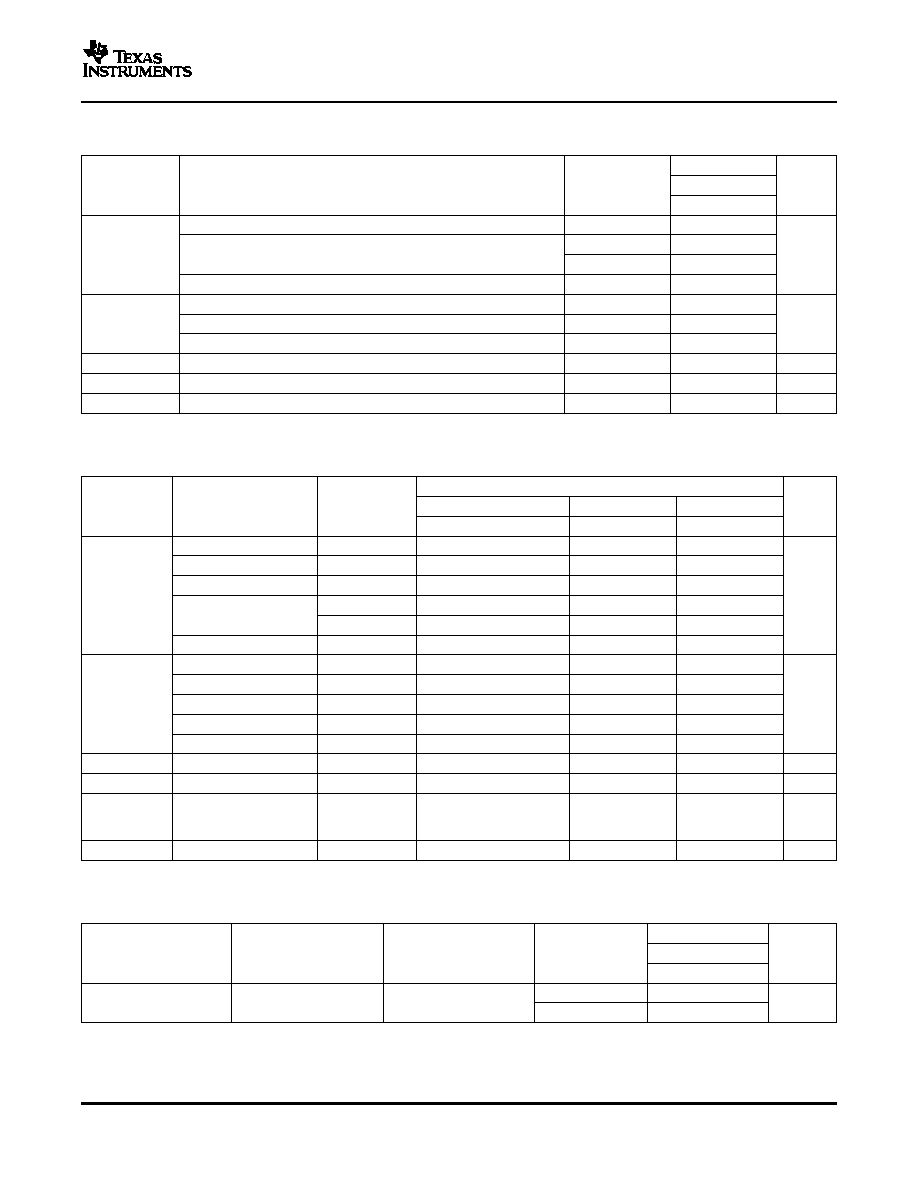
Recommended Operating Conditions
(1)
Recommended Operating Conditions
(1)
SN54LVC04A, SN74LVC04A
HEX INVERTERS
SCAS281R ≠ JANUARY 1993 ≠ REVISED JULY 2005
SN54LVC04A
≠55
į
C to 125įC
UNIT
MIN
MAX
Operating
2
3.6
V
CC
Supply voltage
V
Data retention only
1.5
V
IH
High-level input voltage
V
CC
= 2.7 V to 3.6 V
2
V
V
IL
Low-level input voltage
V
CC
= 2.7 V to 3.6 V
0.8
V
V
I
Input voltage
0
5.5
V
V
O
Output voltage
0
V
CC
V
V
CC
= 2.7 V
≠12
I
OH
High-level output current
mA
V
CC
= 3 V
≠24
V
CC
= 2.7 V
12
I
OL
Low-level output current
mA
V
CC
= 3 V
24
(1)
All unused inputs of the device must be held at V
CC
or GND to ensure proper device operation. Refer to the TI application report,
Implications of Slow or Floating CMOS Inputs, literature number SCBA004.
SN74LVC04A
T
A
= 25įC
≠40
į
C to 85įC
≠40
į
C to 125įC
UNIT
MIN
MAX
MIN
MAX
MIN
MAX
Operating
1.65
3.6
1.65
3.6
1.65
3.6
V
CC
Supply voltage
V
Data retention only
1.5
1.5
1.5
V
CC
= 1.65 V to 1.95 V
0.65 ◊ V
CC
0.65 ◊ V
CC
0.65 ◊ V
CC
High-level
V
IH
V
CC
= 2.3 V to 2.7 V
1.7
1.7
1.7
V
input voltage
V
CC
= 2.7 V to 3.6 V
2
2
2
V
CC
= 1.65 V to 1.95 V
0.35 ◊ V
CC
0.35 ◊ V
CC
0.35 ◊ V
CC
Low-level
V
IL
V
CC
= 2.3 V to 2.7 V
0.7
0.7
0.7
V
input voltage
V
CC
= 2.7 V to 3.6 V
0.8
0.8
0.8
V
I
Input voltage
0
5.5
0
5.5
0
5.5
V
V
O
Output voltage
0
V
CC
0
V
CC
0
V
CC
V
V
CC
= 1.65 V
≠4
≠4
≠4
V
CC
= 2.3 V
≠8
≠8
≠8
High-level
I
OH
mA
output current
V
CC
= 2.7 V
≠12
≠12
≠12
V
CC
= 3 V
≠24
≠24
≠24
V
CC
= 1.65 V
4
4
4
V
CC
= 2.3 V
8
8
8
Low-level
I
OL
mA
output current
V
CC
= 2.7 V
12
12
12
V
CC
= 3 V
24
24
24
(1)
All unused inputs of the device must be held at V
CC
or GND to ensure proper device operation. Refer to the TI application report,
Implications of Slow or Floating CMOS Inputs, literature number SCBA004.
4
www.ti.com
Electrical Characteristics
Electrical Characteristics
Switching Characteristics
SN54LVC04A, SN74LVC04A
HEX INVERTERS
SCAS281R ≠ JANUARY 1993 ≠ REVISED JULY 2005
over recommended operating free-air temperature range (unless otherwise noted)
SN54LVC04A
PARAMETER
TEST CONDITIONS
V
CC
≠55
į
C to 125įC
UNIT
MIN
MAX
I
OH
= ≠100
Ķ
A
2.7 V to 3.6 V
V
CC
≠ 0.2
2.7 V
2.2
V
OH
I
OH
= ≠12 mA
V
3 V
2.4
I
OH
= ≠24 mA
3 V
2.2
I
OL
= 100
Ķ
A
2.7 V to 3.6 V
0.2
V
OL
I
OL
= 12 mA
2.7 V
0.4
V
I
OL
= 24 mA
3 V
0.55
I
I
V
I
= 5.5 V or GND
3.6 V
Ī5
Ķ
A
I
CC
V
I
= V
CC
or GND, I
O
= 0
3.6 V
10
Ķ
A
I
CC
One input at V
CC
≠ 0.6 V, Other inputs at V
CC
or GND
2.7 V to 3.6 V
500
Ķ
A
over recommended operating free-air temperature range (unless otherwise noted)
SN74LVC04A
PARAMETER
TEST CONDITIONS
V
CC
T
A
= 25įC
≠40
į
C to 85įC
≠40
į
C to 125įC
UNIT
MIN
TYP
MAX
MIN
MAX
MIN
MAX
I
OH
= ≠100
Ķ
A
1.65 V to 3.6 V
V
CC
≠ 0.2
V
CC
≠ 0.2
V
CC
≠ 0.3
I
OH
= ≠4 mA
1.65 V
1.29
1.2
1.05
I
OH
= ≠8 mA
2.3 V
1.9
1.7
1.55
V
OH
V
2.7 V
2.2
2.2
2.05
I
OH
= ≠12 mA
3 V
2.4
2.4
2.25
I
OH
= ≠24 mA
3 V
2.3
2.2
2
I
OL
= 100
Ķ
A
1.65 V to 3.6 V
0.1
0.2
0.3
I
OL
= 4 mA
1.65 V
0.24
0.45
0.6
V
OL
I
OL
= 8 mA
2.3 V
0.3
0.7
0.85
V
I
OL
= 12 mA
2.7 V
0.4
0.4
0.6
I
OL
= 24 mA
3 V
0.55
0.55
0.8
I
I
V
I
= 5.5 V or GND
3.6 V
Ī1
Ī5
Ī20
Ķ
A
I
CC
V
I
= V
CC
or GND, I
O
= 0
3.6 V
1
10
40
Ķ
A
One input at V
CC
≠ 0.6 V,
I
CC
Other inputs at V
CC
or
2.7 V to 3.6 V
500
500
5000
Ķ
A
GND
C
i
V
I
= V
CC
or GND
3.3 V
5
pF
over recommended operating free-air temperature range (unless otherwise noted) (see Figure 1)
SN54LVC04A
FROM
TO
PARAMETER
V
CC
≠55
į
C to 125įC
UNIT
(INPUT)
(OUTPUT)
MIN
MAX
2.7 V
5.5
t
pd
A
Y
ns
3.3 V Ī 0.3 V
0.5
4.5
5