SMJ320C31, SMJ320LC31, SMQ320LC31
DIGITAL SIGNAL PROCESSORS
SGUS026F ≠ APRIL 1998 ≠ REVISED OCTOBER 2001
1
POST OFFICE BOX 1443
∑
HOUSTON, TEXAS 77251≠1443
D
Processed to MIL-PRF-38535 (QML)
D
Operating Temperature Ranges:
≠ Military (M) ≠55
∞
C to 125
∞
C
≠ Special (S) ≠55
∞
C to 105
∞
C
D
SMD Approval
D
High-Performance Floating-Point Digital
Signal Processor (DSP):
≠ SMJ320C31-60 (5 V)
33-ns Instruction Cycle Time
330 Million Operations Per Second
(MOPS), 60 Million Floating-Point
Operations Per Second (MFLOPS),
30 Million Instructions Per Second
(MIPS)
≠ SMJ320C31-50 (5 V)
40-ns Instruction Cycle Time
275 MOPS, 50 MFLOPS, 25 MIPS
≠ SMJ320C31-40 (5 V)
50-ns Instruction Cycle Time
220 MOPS, 40 MFLOPS, 20 MIPS
≠ SMJ320LC31-40 (3.3 V)
50-ns Instruction Cycle Time
220 MOPS, 40 MFLOPS, 20 MIPS
≠ SMQ320LC31-40 (3.3 V)
50-ns Instruction Cycle Time
220 MOPS, 40 MFLOPS, 20 MIPS
D
32-Bit High-Performance CPU
D
16- / 32-Bit Integer and 32- / 40-Bit
Floating-Point Operations
D
32-Bit Instruction and Data Words, 24-Bit
Addresses
D
Two 1K Word
◊
32-Bit Single-Cycle
Dual-Access On-Chip RAM Blocks
D
Boot-Program Loader
D
64-Word
◊
32-Bit Instruction Cache
D
Eight Extended-Precision Registers
D
Two Address Generators With Eight
Auxiliary Registers and Two Auxiliary
Register Arithmetic Units (ARAUs)
D
Two Low-Power Modes
D
On-Chip Memory-Mapped Peripherals:
≠ One Serial Port Supporting
8- / 16- / 24- / 32-Bit Transfers
≠ Two 32-Bit Timers
≠ One-Channel Direct Memory Access
(DMA) Coprocessor for Concurrent I/O
and CPU Operation
D
Fabricated Using Enhanced Performance
Implanted CMOS (EPIC
) Technology by
Texas Instruments (TI )
D
Two- and Three-Operand Instructions
D
40 / 32-Bit Floating-Point / Integer Multiplier
and Arithmetic Logic Unit (ALU)
D
Parallel ALU and Multiplier Execution in a
Single Cycle
D
Block-Repeat Capability
D
Zero-Overhead Loops With Single-Cycle
Branches
D
Conditional Calls and Returns
D
Interlocked Instructions for
Multiprocessing Support
D
Bus-Control Registers Configure
Strobe-Control Wait-State Generation
D
Validated Ada Compiler
D
Integer, Floating-Point, and Logical
Operations
D
32-Bit Barrel Shifter
D
One 32-Bit Data Bus (24-Bit Address)
D
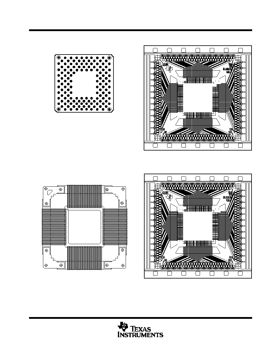
Packaging
≠ 132-Lead Ceramic Quad Flatpack With
Nonconductive Tie-Bar (HFG Suffix)
≠ 141-Pin Ceramic Staggered Pin
Grid- Array Package (GFA Suffix)
≠ 132-Lead TAB Frame
≠ 132-Lead Plastic Quad Flatpack
(PQ Suffix)
description
The SMJ320C31, SMJ320LC31, and SMQ320LC31 digital signal processors (DSPs) are 32-bit, floating-point
processors manufactured in 0.6-
µ
m triple-level-metal CMOS technology. The devices are part of the
SMJ320C3x generation of DSPs from Texas Instruments.
Please be aware that an important notice concerning availability, standard warranty, and use in critical applications of
Texas Instruments semiconductor products and disclaimers thereto appears at the end of this data sheet.
PRODUCTION DATA information is current as of publication date.
Products conform to specifications per the terms of Texas Instruments
standard warranty. Production processing does not necessarily include
testing of all parameters.
EPIC is a trademark of Texas Instruments Incorporated.
Copyright
2001, Texas Instruments Incorporated
On products compliant to MIL-PRF-38535, all parameters are tested
unless otherwise noted. On all other products, production
processing does not necessarily include testing of all parameters.

SMJ320C31, SMJ320LC31, SMQ320LC31
DIGITAL SIGNAL PROCESSORS
SGUS026F ≠ APRIL 1998 ≠ REVISED OCTOBER 2001
2
POST OFFICE BOX 1443
∑
HOUSTON, TEXAS 77251≠1443
description (continued)
The SMJ320C3x internal busing and special digital-signal-processing instruction set have the speed and
flexibility to execute up to 60 MFLOPS. The SMJ320C3x optimizes speed by implementing functions in
hardware that other processors implement through software or microcode. This hardware-intensive approach
provides performance previously unavailable on a single chip.
The SMJ320C3x can perform parallel multiply and ALU operations on integer or floating-point data in a single
cycle. Each processor also possesses a general-purpose register file, a program cache, dedicated ARAUs,
internal dual-access memories, one DMA channel supporting concurrent I/O, and a short machine-cycle time.
High performance and ease of use are results of these features.
General-purpose applications are greatly enhanced by the large address space, multiprocessor interface,
internally and externally generated wait states, one external interface port, two timers, one serial port, and
multiple-interrupt structure. The SMJ320C3x supports a wide variety of system applications from host processor
to dedicated coprocessor.
High-level-language support is easily implemented through a register-based architecture, large address space,
powerful addressing modes, flexible instruction set, and well-supported floating-point arithmetic.
For additional information when designing for cold temperature operation, please see Texas Instruments
application report 320C3x, 320C4x and 320MCM42x Power-up Sensitivity at Cold Temperature, literature
number SGUA001.
SMJ320C31, SMJ320LC31, SMQ320LC31
DIGITAL SIGNAL PROCESSORS
SGUS026F ≠ APRIL 1998 ≠ REVISED OCTOBER 2001
5
POST OFFICE BOX 1443
∑
HOUSTON, TEXAS 77251≠1443
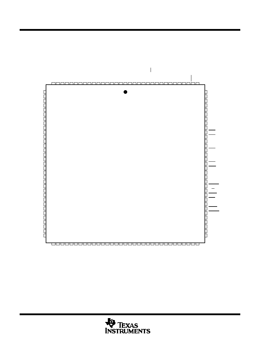
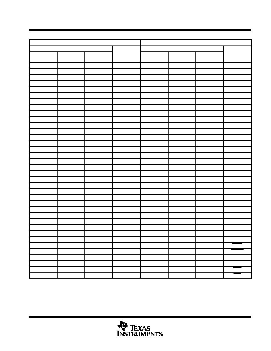
Terminal Assignments
PIN
PIN
NUMBER
NUMBER
PQ
PKG
HFG
PKG
GFA
PKG
NAME
PQ
PKG
HFG
PKG
GFA
PKG
NAME
29
12
L1
A0
64
47
W9
D10
28
11
K2
A1
63
46
U9
D11
27
10
J1
A2
62
45
V8
D12
26
9
J3
A3
60
43
W7
D13
25
8
G1
A4
58
41
U7
D14
23
6
F2
A5
56
39
V6
D15
22
5
E1
A6
55
38
W5
D16
21
4
E3
A7
54
37
U5
D17
20
3
D2
A8
53
36
V4
D18
18
1
C1
A9
52
35
W3
D19
16
131
C3
A10
50
33
U3
D20
14
129
B2
A11
48
31
V2
D21
13
128
A1
A12
47
30
W1
D22
12
127
C5
A13
46
29
R3
D23
11
126
B4
A14
45
28
T2
D24
10
125
A3
A15
44
27
U1
D25
9
124
C7
A16
43
26
N3
D26
8
123
B6
A17
41
24
P2
D27
7
122
C9
A18
39
22
R1
D28
5
120
B8
A19
38
21
L3
D29
2
117
A7
A20
34
17
M2
D30
1
116
A9
A21
31
14
N1
D31
130
113
B10
A22
108
91
C19
DR0
129
112
A11
A23
116
99
C17
DX0
111
94
E17
CLKR0
124
107
B14
EMU0
112
95
A19
CLKX0
125
108
A13
EMU1
80
63
W19
D0
126
109
B12
EMU2
79
62
V16
D1
123
106
A15
EMU3
78
61
W17
D2
110
93
D18
FSR0
77
60
U13
D3
114
97
B18
FSX0
76
59
V14
D4
81
73
P18
HOLD
75
58
W15
D5
82
72
R19
HOLDA
73
56
U11
D6
90
64
V18
H1
72
55
V12
D7
89
65
U17
H3
68
51
W11
D8
99
82
H18
IACK
67
50
V10
D9
100
83
J17
INT0
CVSS, VSSL, and IVSS are on the same plane.
AVDD, DVDD, CVDD, and PVDD are on the same plane.
ß VSUBS connects to die metallization. Tie this pin to clean ground.