SN54LVC74A, SN74LVC74A
DUAL POSITIVE EDGE TRIGGERED D TYPE FLIP FLOPS
WITH CLEAR AND PRESET
SCAS287Q - JANUARY 1993 - REVISED JULY 2003
1
POST OFFICE BOX 655303
∑
DALLAS, TEXAS 75265
D
Operate From 1.65 V to 3.6 V
D
Inputs Accept Voltages to 5.5 V
D
Max t
pd
of 5.2 ns at 3.3 V
D
Typical V
OLP
(Output Ground Bounce)
<0.8 V at V
CC
= 3.3 V, T
A
= 25
∞
C
D
Typical V
OHV
(Output V
OH
Undershoot)
>2 V at V
CC
= 3.3 V, T
A
= 25
∞
C
D
Latch-Up Performance Exceeds 250 mA Per
JESD 17
D
ESD Protection Exceeds JESD 22
- 2000-V Human-Body Model (A114-A)
- 200-V Machine Model (A115-A)
- 1000-V Charged-Device Model (C101)
description/ordering information
The SN54LVC74A dual positive-edge-triggered D-type flip-flop is designed for 2.7-V to 3.6-V V
CC
operation,
and the SN74LVC74A dual positive-edge-triggered D-type flip-flop is designed for 1.65-V to 3.6-V V
CC
operation.
ORDERING INFORMATION
TA
PACKAGE
ORDERABLE
PART NUMBER
TOP-SIDE MARKING
QFN - RGY
Reel of 1000
SN74LVC74ARGYR
LC74A
Tube of 50
SN74LVC74AD
SOIC - D
Reel of 2500
SN74LVC74ADR
LVC74A
SOIC - D
Reel of 250
SN74LVC74ADT
LVC74A
-40
∞
C to 85
∞
C
SOP - NS
Reel of 2000
SN74LVC74ANSR
LCV74A
-40 C to 85 C
SSOP - DB
Reel of 2000
SN74LVC74ADBR
LC74A
Tube of 90
SN74LVC74APW
TSSOP - PW
Reel of 2000
SN74LVC74APWR
LC74A
TSSOP - PW
Reel of 250
SN74LVC74APWT
LC74A
CDIP - J
Tube of 25
SNJ54LVC74AJ
SNJ54LVC74AJ
-55
∞
C to 125
∞
C
CFP - W
Tube of 150
SNJ54LVC74AW
SNJ54LVC74AW
-55 C to 125 C
LCCC - FK
Tube of 55
SNJ54LVC74AFK
SNJ54LVC74AFK
Package drawings, standard packing quantities, thermal data, symbolization, and PCB design guidelines are
available at www.ti.com/sc/package.
Copyright
2003, Texas Instruments Incorporated
PRODUCTION DATA information is current as of publication date.
Products conform to specifications per the terms of Texas Instruments
standard warranty. Production processing does not necessarily include
testing of all parameters.
Please be aware that an important notice concerning availability, standard warranty, and use in critical applications of
Texas Instruments semiconductor products and disclaimers thereto appears at the end of this data sheet.
1
2
3
4
5
6
7
14
13
12
11
10
9
8
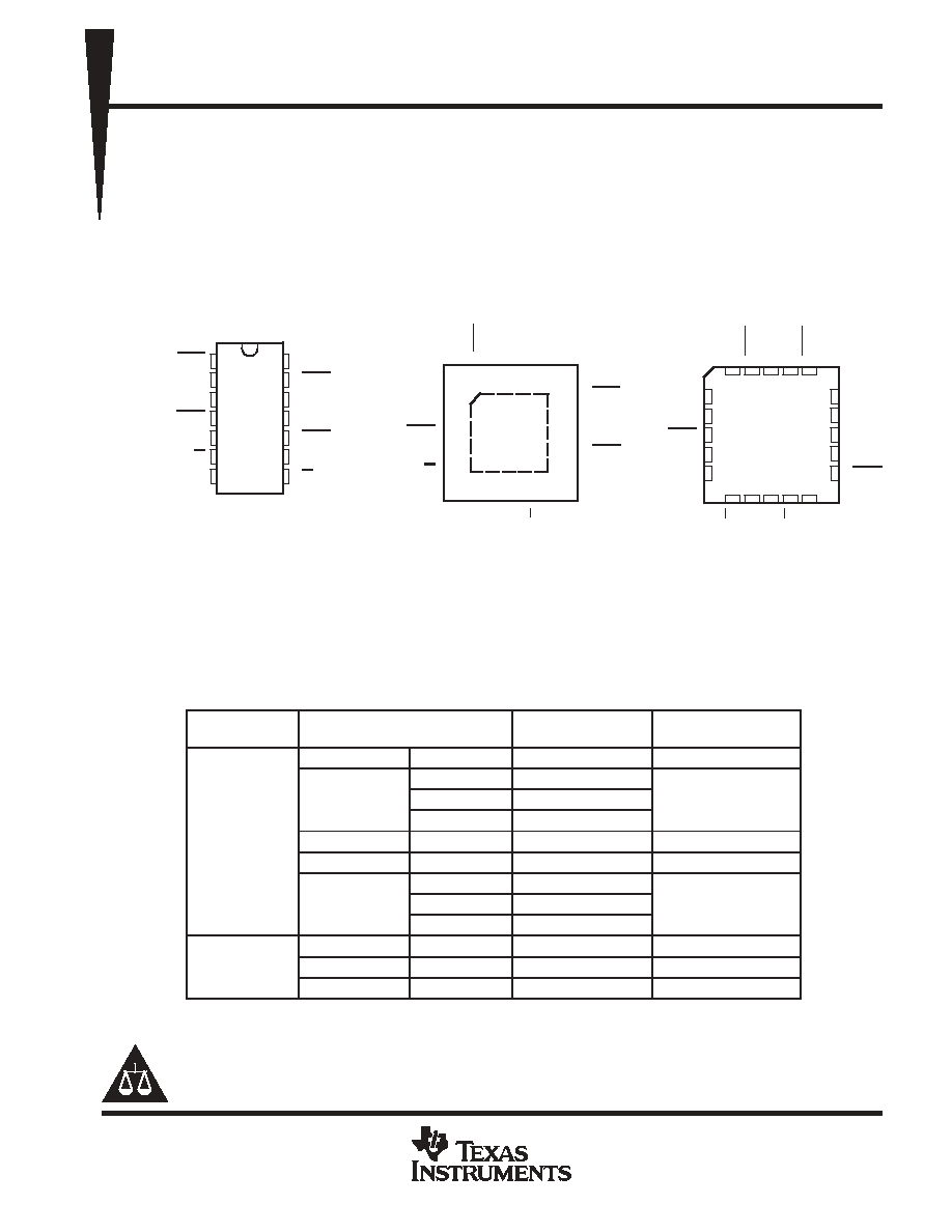
1CLR
1D
1CLK
1PRE
1Q
1Q
GND
V
CC
2CLR
2D
2CLK
2PRE
2Q
2Q
SN54LVC74A . . . J OR W PACKAGE
SN74LVC74A . . . D, DB, NS, OR PW PACKAGE
(TOP VIEW)
3
2 1 20 19
9 10 11 12 13
4
5
6
7
8
18
17
16
15
14
2D
NC
2CLK
NC
2PRE
1CLK
NC
1PRE
NC
1Q
1D
1CLR
NC
2Q
2Q
V
2CLR
1Q
GND
NC
SN54LVC74A . . . FK PACKAGE
(TOP VIEW)
CC
NC - No internal connection
SN74LVC74A . . . RGY PACKAGE
(TOP VIEW)
1
14
7
8
2
3
4
5
6
13
12
11
10
9
2CLR
2D
2CLK
2PRE
2Q
1D
1CLK
1PRE
1Q
1Q
1CLR
2Q
V
GND
CC
On products compliant to MIL PRF 38535, all parameters are tested
unless otherwise noted. On all other products, production
processing does not necessarily include testing of all parameters.
SN54LVC74A, SN74LVC74A
DUAL POSITIVE EDGE TRIGGERED D TYPE FLIP FLOPS
WITH CLEAR AND PRESET
SCAS287Q - JANUARY 1993 - REVISED JULY 2003
2
POST OFFICE BOX 655303
∑
DALLAS, TEXAS 75265
description/ordering information (continued)
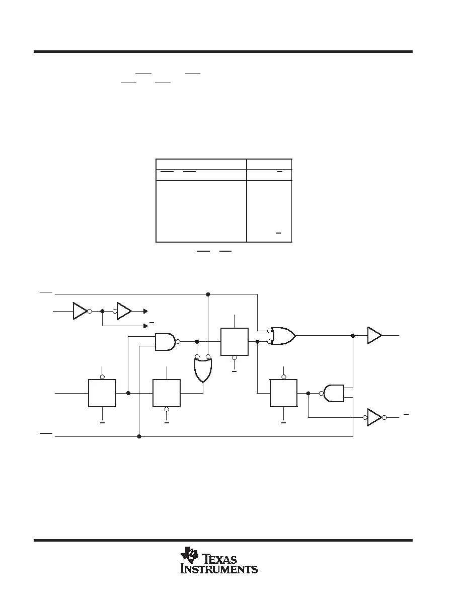
A low level at the preset (PRE) or clear (CLR) inputs sets or resets the outputs, regardless of the levels of the
other inputs. When PRE and CLR are inactive (high), data at the data (D) input meeting the setup time
requirements is transferred to the outputs on the positive-going edge of the clock pulse. Clock triggering occurs
at a voltage level and is not directly related to the rise time of the clock pulse. Following the hold-time interval,
data at the D input can be changed without affecting the levels at the outputs.
Inputs can be driven from either 3.3-V or 5-V devices. This feature allows the use of these devices as translators
in a mixed 3.3-V/5-V system environment.
FUNCTION TABLE
INPUTS
OUTPUTS
PRE
CLR
CLK
D
Q
Q
L
H
X
X
H
L
H
L
X
X
L
H
L
L
X
X
H
H
H
H
H
H
L
H
H
L
L
H
H
H
L
X
Q0
Q0
This configuration is nonstable; that is, it does not
persist when PRE or CLR returns to its inactive
(high) level.
logic diagram, each flip-flop (positive logic)
TG
C
C
TG
C
C
TG
C
C
C
TG
C
C
PRE
CLK
D
CLR
Q
Q
C
SN54LVC74A, SN74LVC74A
DUAL POSITIVE EDGE TRIGGERED D TYPE FLIP FLOPS
WITH CLEAR AND PRESET
SCAS287Q - JANUARY 1993 - REVISED JULY 2003
3
POST OFFICE BOX 655303
∑
DALLAS, TEXAS 75265
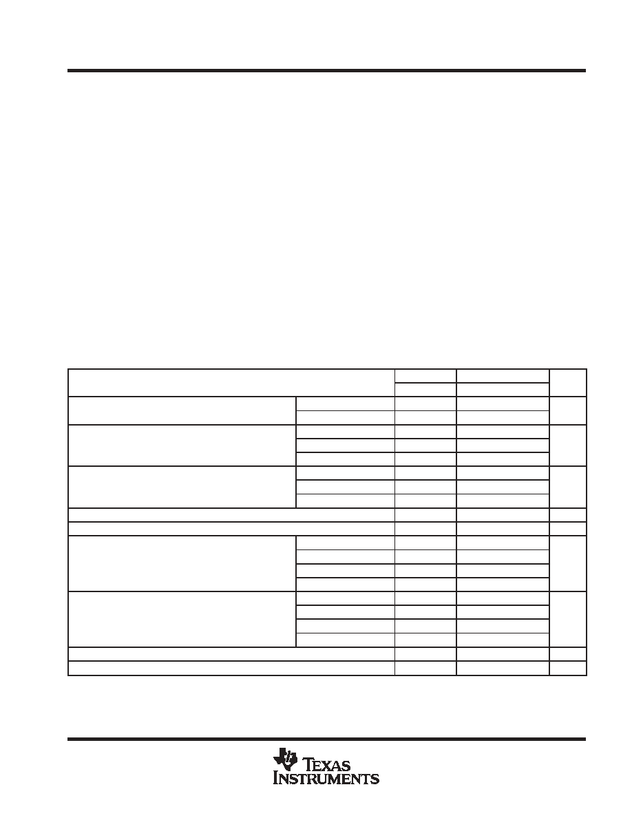
absolute maximum ratings over operating free-air temperature range (unless otherwise noted)
Supply-voltage range, V
CC
-0.5 V to 6.5 V
. . . . . . . . . . . . . . . . . . . . . . . . . . . . . . . . . . . . . . . . . . . . . . . . . . . . . . . . .
Input-voltage range, V
I
(see Note 1)
-0.5 V to 6.5 V
. . . . . . . . . . . . . . . . . . . . . . . . . . . . . . . . . . . . . . . . . . . . . . . . .
Output-voltage range, V
O
(see Notes 1 and 2)
-0.5 V to V
CC
+ 0.5 V
. . . . . . . . . . . . . . . . . . . . . . . . . . . . . . . . . .
Input clamp current, I
IK
(V
I
< 0)
-50 mA
. . . . . . . . . . . . . . . . . . . . . . . . . . . . . . . . . . . . . . . . . . . . . . . . . . . . . . . . . . .
Output clamp current, I
OK
(V
O
< 0)
-50 mA
. . . . . . . . . . . . . . . . . . . . . . . . . . . . . . . . . . . . . . . . . . . . . . . . . . . . . . . .
Continuous output current, I
O
±
50 mA
. . . . . . . . . . . . . . . . . . . . . . . . . . . . . . . . . . . . . . . . . . . . . . . . . . . . . . . . . . . . .
Continuous current through V
CC
or GND
±
100 mA
. . . . . . . . . . . . . . . . . . . . . . . . . . . . . . . . . . . . . . . . . . . . . . . . . .
Package thermal impedance,
JA
(see Note 3): D package
86
∞
C/W
. . . . . . . . . . . . . . . . . . . . . . . . . . . . . . . . . . .
(see Note 3): DB package
96
∞
C/W
. . . . . . . . . . . . . . . . . . . . . . . . . . . . . . . . .
(see Note 3): NS package
76
∞
C/W
. . . . . . . . . . . . . . . . . . . . . . . . . . . . . . . . .
(see Note 3): PW package
113
∞
C/W
. . . . . . . . . . . . . . . . . . . . . . . . . . . . . . . .
(see Note 4): RGY package
47
∞
C/W
. . . . . . . . . . . . . . . . . . . . . . . . . . . . . . . .
Storage temperature range, T
stg
-65
∞
C to 150
∞
C
. . . . . . . . . . . . . . . . . . . . . . . . . . . . . . . . . . . . . . . . . . . . . . . . . . .
Stresses beyond those listed under "absolute maximum ratings" may cause permanent damage to the device. These are stress ratings only, and
functional operation of the device at these or any other conditions beyond those indicated under "recommended operating conditions" is not
implied. Exposure to absolute-maximum-rated conditions for extended periods may affect device reliability.
NOTES:
1. The input negative-voltage and output voltage ratings may be exceeded if the input and output current ratings are observed.
2. The value of VCC is provided in the recommended operating conditions table.
3. The package thermal impedance is calculated in accordance with JESD 51-7.
4. The package thermal impedance is calculated in accordance with JESD 51-5.
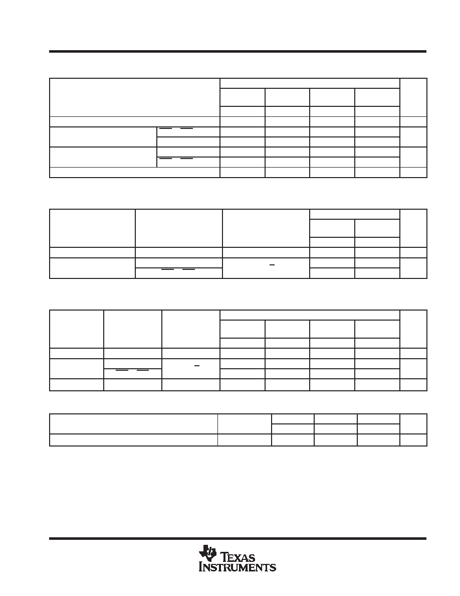
recommended operating conditions (see Note 5)
SN54LVC74A
SN74LVC74A
UNIT
MIN
MAX
MIN
MAX
UNIT
VCC
Supply voltage
Operating
2
3.6
1.65
3.6
V
VCC
Supply voltage
Data retention only
1.5
1.5
V
VCC = 1.65 V to 1.95 V
0.65
◊
VCC
VIH
High-level input voltage
VCC = 2.3 V to 2.7 V
1.7
V
VIH
High-level input voltage
VCC = 2.7 V to 3.6 V
2
2
V
VCC = 1.65 V to 1.95 V
0.35
◊
VCC
VIL
Low-level input voltage
VCC = 2.3 V to 2.7 V
0.7
V
VIL
Low-level input voltage
VCC = 2.7 V to 3.6 V
0.8
0.8
V
VI
Input voltage
0
5.5
0
5.5
V
VO
Output voltage
0
VCC
0
VCC
V
VCC = 1.65 V
-4
IOH
High-level output current
VCC = 2.3 V
-8
mA
IOH
High-level output current
VCC = 2.7 V
-12
-12
mA
VCC = 3 V
-24
-24
VCC = 1.65 V
4
IOL
Low-level output current
VCC = 2.3 V
8
mA
IOL
Low-level output current
VCC = 2.7 V
12
12
mA
VCC = 3 V
24
24
t/
v
Input transition rise or fall rate
10
10
ns/V
TA
Operating free-air temperature
-55
125
-40
85
∞
C
NOTE 5: All unused inputs of the device must be held at VCC or GND to ensure proper device operation. Refer to the TI application report,
Implications of Slow or Floating CMOS Inputs, literature number SCBA004.
SN54LVC74A, SN74LVC74A
DUAL POSITIVE EDGE TRIGGERED D TYPE FLIP FLOPS
WITH CLEAR AND PRESET
SCAS287Q - JANUARY 1993 - REVISED JULY 2003
4
POST OFFICE BOX 655303
∑
DALLAS, TEXAS 75265
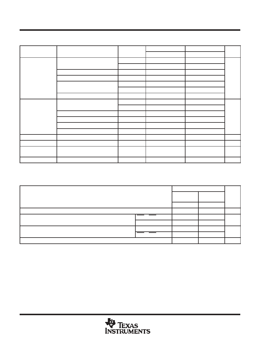
electrical characteristics over recommended operating free-air temperature range (unless
otherwise noted)
PARAMETER
TEST CONDITIONS
VCC
SN54LVC74A
SN74LVC74A
UNIT
PARAMETER
TEST CONDITIONS
VCC
MIN
TYP
MAX
MIN
TYP
MAX
UNIT
IOH = -100 A
1.65 V to 3.6 V
VCC-0.2
IOH = -100
µ
A
2.7 V to 3.6 V
VCC-0.2
IOH = -4 mA
1.65 V
1.2
VOH
IOH = -8 mA
2.3 V
1.7
V
VOH
IOH = -12 mA
2.7 V
2.2
2.2
V
IOH = -12 mA
3 V
2.4
2.4
IOH = -24 mA
3 V
2.2
2.2
IOL = 100 A
1.65 V to 3.6 V
0.2
IOL = 100
µ
A
2.7 V to 3.6 V
0.2
VOL
IOL = 4 mA
1.65 V
0.45
V
VOL
IOL = 8 mA
2.3 V
0.7
V
IOL = 12 mA
2.7 V
0.4
0.4
IOL = 24 mA
3 V
0.55
0.55
II
VI = 5.5 V or GND
3.6 V
±
5
±
5
µ
A
ICC
VI = VCC or GND,
IO = 0
3.6 V
10
10
µ
A
ICC
One input at VCC - 0.6 V,
Other inputs at VCC or GND
2.7 V to 3.6 V
500
500
µ
A
Ci
VI = VCC or GND
3.3 V
5
5
pF
All typical values are at VCC = 3.3 V, TA = 25
∞
C.
timing requirements over recommended operating free-air temperature range (unless otherwise
noted) (see Figure 1)
SN54LVC74A
VCC = 2.7 V
VCC = 3.3 V
±
0.3 V
UNIT
MIN
MAX
MIN
MAX
fclock
Clock frequency
83
100
MHz
tw
Pulse duration
PRE or CLR low
3.3
3.3
ns
tw
Pulse duration
CLK high or low
3.3
3.3
ns
tsu
Setup time before CLK
Data
3.4
3
ns
tsu
Setup time before CLK
PRE or CLR inactive
2.2
2
ns
th
Hold time, data after CLK
1
1
ns
SN54LVC74A, SN74LVC74A
DUAL POSITIVE EDGE TRIGGERED D TYPE FLIP FLOPS
WITH CLEAR AND PRESET
SCAS287Q - JANUARY 1993 - REVISED JULY 2003
5
POST OFFICE BOX 655303
∑
DALLAS, TEXAS 75265
timing requirements over recommended operating free-air temperature range (unless otherwise
noted) (see Figure 1)
SN74LVC74A
VCC = 1.8 V
±
0.15 V
VCC = 2.5 V
±
0.2 V
VCC = 2.7 V
VCC = 3.3 V
±
0.3 V
UNIT
MIN
MAX
MIN
MAX
MIN
MAX
MIN
MAX
fclock
Clock frequency
83
83
83
100
MHz
tw
Pulse duration
PRE or CLR low
4.1
3.3
3.3
3.3
ns
tw
Pulse duration
CLK high or low
4.1
3.3
3.3
3.3
ns
tsu
Setup time before CLK
Data
3.6
2.3
3.4
3
ns
tsu
Setup time before CLK
PRE or CLR inactive
2.7
1.9
2.2
2
ns
th
Hold time, data after CLK
1
1
1
0
ns
switching characteristics over recommended operating free-air temperature range (unless
otherwise noted) (see Figure 1)
SN54LVC74A
PARAMETER
FROM
(INPUT)
TO
(OUTPUT)
VCC = 2.7 V
VCC = 3.3 V
±
0.3 V
UNIT
(INPUT)
(OUTPUT)
MIN
MAX
MIN
MAX
fmax
83
100
MHz
tpd
CLK
Q or Q
6
1
5.2
ns
tpd
PRE or CLR
Q or Q
6.4
1
5.4
ns
switching characteristics over recommended operating free-air temperature range (unless
otherwise noted) (see Figure 1)
SN74LVC74A
PARAMETER
FROM
(INPUT)
TO
(OUTPUT)
VCC = 1.8 V
±
0.15 V
VCC = 2.5 V
±
0.2 V
VCC = 2.7 V
VCC = 3.3 V
±
0.3 V
UNIT
(INPUT)
(OUTPUT)
MIN
MAX
MIN
MAX
MIN
MAX
MIN
MAX
fmax
83
83
83
100
MHz
tpd
CLK
Q or Q
1
7.1
1
4.4
1
6
1
5.2
ns
tpd
PRE or CLR
Q or Q
1
6.9
1
4.6
1
6.4
1
5.4
ns
tsk(o)
1
ns
operating characteristics, T
A
= 25
∞
C
PARAMETER
TEST
VCC = 1.8 V
VCC = 2.5 V
VCC = 3.3 V
UNIT
PARAMETER
TEST
CONDITIONS
TYP
TYP
TYP
UNIT
Cpd
Power dissipation capacitance per flip-flop
f = 10 MHz
47
47
51
pF