SN54LVC652A, SN74LVC652A
OCTAL BUS TRANSCEIVERS AND REGISTERS
WITH 3 STATE OUTPUTS
SCAS303L - JANUARY 1993 - REVISED AUGUST 2003
1
POST OFFICE BOX 655303
∑
DALLAS, TEXAS 75265
D
Operate From 1.65 V to 3.6 V
D
Inputs Accept Voltages to 5.5 V
D
Max t
pd
of 7.4 ns at 3.3 V
D
Typical V
OLP
(Output Ground Bounce)
<0.8 V at V
CC
= 3.3 V, T
A
= 25
∞
C
D
Typical V
OHV
(Output V
OH
Undershoot)
>2 V at V
CC
= 3.3 V, T
A
= 25
∞
C
D
Support Mixed-Mode Signal Operation on
All Ports (5-V Input/Output Voltage With
3.3-V V
CC
)
D
I
off
Supports Partial-Power-Down Mode
Operation
D
ESD Protection Exceeds JESD 22
- 2000-V Human-Body Model (A114-A)
- 200-V Machine Model (A115-A)
- 1000-V Charged-Device Model (C101)
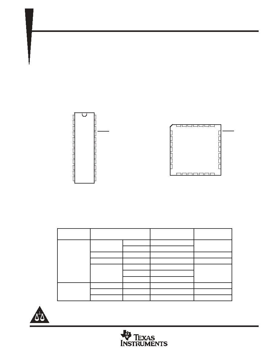
SN54LVC652A . . . JT OR W PACKAGE
SN74LVC652A . . . DB, DW, NS, OR PW PACKAGE
(TOP VIEW)
1
2
3
4
5
6
7
8
9
10
11
12
24
23
22
21
20
19
18
17
16
15
14
13
CLKAB
SAB
OEAB
A1
A2
A3
A4
A5
A6
A7
A8
GND
V
CC
CLKBA
SBA
OEBA
B1
B2
B3
B4
B5
B6
B7
B8
SN54LVC652A . . . FK PACKAGE
(TOP VIEW)
3 2 1 28 27
12 13
5
6
7
8
9
10
11
25
24
23
22
21
20
19
OEBA
B1
B2
NC
B3
B4
B5
A1
A2
A2
NC
A4
A5
A6
4
26
14 15 16 17 18
A7
A8
GND
NC
B8
B7
B6
OEAB
SAB
CLKAB
NC
CLKBA
SBA
V
CC
NC - No internal connection
description/ordering information
The SN54LVC652A octal bus transceiver and register is designed for 2.7-V to 3.6-V V
CC
operation, and the
SN74LVC652A octal bus transceiver and register is designed for 1.65-V to 3.6-V V
CC
operation.
ORDERING INFORMATION
TA
PACKAGE
ORDERABLE
PART NUMBER
TOP-SIDE
MARKING
SOIC - DW
Tube of 25
SN74LVC652ADW
LVC652A
SOIC - DW
Reel of 2000
SN74LVC652ADWR
LVC652A
SOP - NS
Reel of 2000
SN74LVC652ANSR
LVC652A
-40
∞
C to 85
∞
C
SSOP - DB
Reel of 2000
SN74LVC652ADBR
LC652A
-40 C to 85 C
Tube of 60
SN74LVC652APW
TSSOP - PW
Reel of 2000
SN74LVC652APWR
LC652A
TSSOP - PW
Reel of 250
SN74LVC652APWT
LC652A
CDIP - JT
Tube of 15
SNJ54LVC652AJT
SNJ54LVC652AJT
-55
∞
C to 125
∞
C
CFP - W
Tube of 85
SNJ54LVC652AW
SNJ54LVC652AW
-55 C to 125 C
LCCC - FK
Tube of 42
SNJ54LVC652AFK
SNJ54LVC652AFK
Package drawings, standard packing quantities, thermal data, symbolization, and PCB design guidelines are
available at www.ti.com/sc/package.
Copyright
2003, Texas Instruments Incorporated
PRODUCTION DATA information is current as of publication date.
Products conform to specifications per the terms of Texas Instruments
standard warranty. Production processing does not necessarily include
testing of all parameters.
Please be aware that an important notice concerning availability, standard warranty, and use in critical applications of
Texas Instruments semiconductor products and disclaimers thereto appears at the end of this data sheet.
On products compliant to MIL PRF 38535, all parameters are tested
unless otherwise noted. On all other products, production
processing does not necessarily include testing of all parameters.

SN54LVC652A, SN74LVC652A
OCTAL BUS TRANSCEIVERS AND REGISTERS
WITH 3 STATE OUTPUTS
SCAS303L - JANUARY 1993 - REVISED AUGUST 2003
2
POST OFFICE BOX 655303
∑
DALLAS, TEXAS 75265
description/ordering information (continued)
These devices consist of bus transceiver circuits, D-type flip-flops, and control circuitry arranged for multiplexed
transmission of data directly from the data bus or from the internal storage registers.
Output-enable (OEAB and OEBA) inputs are provided to control the transceiver functions. Select-control (SAB
and SBA) inputs are provided to select whether real-time or stored data is transferred. The circuitry used for
select control eliminates the typical decoding glitch that occurs in a multiplexer during the transition between
stored and real-time data. A low input selects real-time data, and a high input selects stored data. Figure 1
illustrates the four fundamental bus-management functions that are performed with the 'LVC652A devices.
Data on the A or B data bus, or both, is stored in the internal D-type flip-flops by low-to-high transitions at the
appropriate clock (CLKAB or CLKBA) inputs, regardless of the select- or enable-control pins. When SAB and
SBA are in the real-time transfer mode, it is possible to store data without using the internal D-type flip-flops by
simultaneously enabling OEAB and OEBA. In this configuration, each output reinforces its input. When all other
data sources to the two sets of bus lines are at high impedance, each set of bus lines remains at its last state.
Inputs can be driven from either 3.3-V or 5-V devices. This feature allows the use of these devices as translators
in a mixed 3.3-V/5-V system environment.
These devices are fully specified for partial-power-down applications using I
off
. The I
off
circuitry disables the
outputs, preventing damaging current backflow through the device when it is powered down.
To ensure the high-impedance state during power up or power down, OEBA should be tied to V
CC
through a
pullup resistor and OEAB should be tied to GND through a pulldown resistor; the minimum value of the resistor
is determined by the current-sinking/current-sourcing capability of the driver.
FUNCTION TABLE
INPUTS
DATA I/O
OPERATION OR FUNCTION
OEAB
OEBA
CLKAB
CLKBA
SAB
SBA
A1-A8
B1-B8
OPERATION OR FUNCTION
L
H
H or L
H or L
X
X
Input
Input
Isolation
L
H
X
X
Input
Input
Store A and B data
X
H
H or L
X
X
Input
Unspecified
Store A, hold B
H
H
X
X
Input
Output
Store A in both registers
L
X
H or L
X
X
Unspecified
Input
Hold A, store B
L
L
X
X
Output
Input
Store B in both registers
L
L
X
X
X
L
Output
Input
Real-time B data to A bus
L
L
X
H or L
X
H
Output
Input
Stored B data to A bus
H
H
X
X
L
X
Input
Output
Real-time A data to B bus
H
H
H or L
X
H
X
Input
Output
Stored A data to B bus
H
L
H or L
H or L
H
H
Output
Output
Stored A data to B bus and
stored B data to A bus
The data-output functions can be enabled or disabled by a variety of level combinations at OEAB or OEBA. Data-input functions always are
enabled; i.e., data at the bus terminals is stored on every low-to-high transition of the clock inputs.
Select control = L; clocks can occur simultaneously.
Select control = H; clocks must be staggered to load both registers.

SN54LVC652A, SN74LVC652A
OCTAL BUS TRANSCEIVERS AND REGISTERS
WITH 3 STATE OUTPUTS
SCAS303L - JANUARY 1993 - REVISED AUGUST 2003
3
POST OFFICE BOX 655303
∑
DALLAS, TEXAS 75265
BUS B
BUS A
BUS B
BUS A
BUS B
BUS A
BUS B
BUS A
OEAB
X
L
L
OEAB
L
L
CLKAB
X
CLKBA
X
SAB
X
SBA
L
CLKAB
X
CLKBA
X
SAB
L
SBA
X
H
CLKAB CLKBA
X
SAB
X
SBA
X
CLKAB
CLKBA
SAB
SBA
X
H
X
X
X
X
X
H
L
H or L
H
H
OEBA
OEBA
H
H
OEAB OEBA
OEAB
OEBA
H or L
REAL-TIME TRANSFER
BUS B TO BUS A
REAL-TIME TRANSFER
BUS A TO BUS B
STORAGE FROM
A, B, OR A AND B
TRANSFER STORED DATA
TO A AND/OR B
3
21
1
23
2
22
1
23
2
22
3
21
3
21
23
2
22
3
21
1
2
22
1
23
Figure 1. Bus-Management Functions

SN54LVC652A, SN74LVC652A
OCTAL BUS TRANSCEIVERS AND REGISTERS
WITH 3 STATE OUTPUTS
SCAS303L - JANUARY 1993 - REVISED AUGUST 2003
4
POST OFFICE BOX 655303
∑
DALLAS, TEXAS 75265
logic diagram (positive logic)
OEBA
A1
B1
1D
C1
1D
C1
One of Eight Channels
SAB
CLKAB
SBA
CLKBA
OEAB
To Seven Other Channels
21
3
23
22
1
2
4
20
Pin numbers shown are for the DB, DW, JT, NS, PW, and W packages.

SN54LVC652A, SN74LVC652A
OCTAL BUS TRANSCEIVERS AND REGISTERS
WITH 3 STATE OUTPUTS
SCAS303L - JANUARY 1993 - REVISED AUGUST 2003
5
POST OFFICE BOX 655303
∑
DALLAS, TEXAS 75265
absolute maximum ratings over operating free-air temperature range (unless otherwise noted)
Supply voltage range, V
CC
-0.5 V to 6.5 V
. . . . . . . . . . . . . . . . . . . . . . . . . . . . . . . . . . . . . . . . . . . . . . . . . . . . . . . . .
Input voltage range, V
I
(see Note 1)
-0.5 V to 6.5 V
. . . . . . . . . . . . . . . . . . . . . . . . . . . . . . . . . . . . . . . . . . . . . . . . .
Voltage range applied to any output in the high-impedance or power-off state, V
O
(see Note 1)
-0.5 V to 6.5 V
. . . . . . . . . . . . . . . . . . . . . . . . . . . . . . . . . . . . . . . . . . . . . . . . . . . . . . . . . . . . . . . . . . .
Voltage range applied to any output in the high or low state, V
O
(see Notes 1 and 2)
-0.5 V to V
CC
+ 0.5 V
. . . . . . . . . . . . . . . . . . . . . . . . . . . . . . . . . . . . . . . . . . . . . . . . . . . . . . .
Input clamp current, I
IK
(V
I
< 0)
-50 mA
. . . . . . . . . . . . . . . . . . . . . . . . . . . . . . . . . . . . . . . . . . . . . . . . . . . . . . . . . . .
Output clamp current, I
OK
(V
O
< 0)
-50 mA
. . . . . . . . . . . . . . . . . . . . . . . . . . . . . . . . . . . . . . . . . . . . . . . . . . . . . . . .
Continuous output current, I
O
±
50 mA
. . . . . . . . . . . . . . . . . . . . . . . . . . . . . . . . . . . . . . . . . . . . . . . . . . . . . . . . . . . . .
Continuous current through V
CC
or GND
±
100 mA
. . . . . . . . . . . . . . . . . . . . . . . . . . . . . . . . . . . . . . . . . . . . . . . . . .
Package thermal impedance,
JA
(see Note 3): DB package
63
∞
C/W
. . . . . . . . . . . . . . . . . . . . . . . . . . . . . . . . .
DW package
46
∞
C/W
. . . . . . . . . . . . . . . . . . . . . . . . . . . . . . . . .
NS package
65
∞
C/W
. . . . . . . . . . . . . . . . . . . . . . . . . . . . . . . . .
PW package
88
∞
C/W
. . . . . . . . . . . . . . . . . . . . . . . . . . . . . . . . .
Storage temperature range, T
stg
-65
∞
C to 150
∞
C
. . . . . . . . . . . . . . . . . . . . . . . . . . . . . . . . . . . . . . . . . . . . . . . . . . .
Stresses beyond those listed under "absolute maximum ratings" may cause permanent damage to the device. These are stress ratings only, and
functional operation of the device at these or any other conditions beyond those indicated under "recommended operating conditions" is not
implied. Exposure to absolute-maximum-rated conditions for extended periods may affect device reliability.
NOTES:
1. The input negative-voltage and output voltage ratings may be exceeded if the input and output current ratings are observed.
2. The value of VCC is provided in the recommended operating conditions table.
3. The package thermal impedance is calculated in accordance with JESD 51-7.
recommended operating conditions (see Note 4)
SN54LVC652A
SN74LVC652A
UNIT
MIN
MAX
MIN
MAX
UNIT
VCC
Supply voltage
Operating
2
3.6
1.65
3.6
V
VCC
Supply voltage
Data retention only
1.5
1.5
V
VCC = 1.65 V to 1.95 V
0.65
◊
VCC
VIH
High-level input voltage
VCC = 2.3 V to 2.7 V
1.7
V
VIH
High-level input voltage
VCC = 2.7 V to 3.6 V
2
2
V
VCC = 1.65 V to 1.95 V
0.35
◊
VCC
VIL
Low-level input voltage
VCC = 2.3 V to 2.7 V
0.7
V
VIL
Low-level input voltage
VCC = 2.7 V to 3.6 V
0.8
0.8
V
VI
Input voltage
0
5.5
0
5.5
V
VO
Output voltage
High or low state
0
VCC
0
VCC
V
VO
Output voltage
3-state
0
5.5
0
5.5
V
VCC = 1.65 V
-4
IOH
High-level output current
VCC = 2.3 V
-8
mA
IOH
High-level output current
VCC = 2.7 V
-12
-12
mA
VCC = 3 V
-24
-24
VCC = 1.65 V
4
IOL
Low-level output current
VCC = 2.3 V
8
mA
IOL
Low-level output current
VCC = 2.7 V
12
12
mA
VCC = 3 V
24
24
t/
v
Input transition rise or fall rate
5
5
ns/V
TA
Operating free-air temperature
-55
125
-40
85
∞
C
NOTE 4: All unused inputs of the device must be held at VCC or GND to ensure proper device operation. Refer to the TI application report,
Implications of Slow or Floating CMOS Inputs, literature number SCBA004.

SN54LVC652A, SN74LVC652A
OCTAL BUS TRANSCEIVERS AND REGISTERS
WITH 3 STATE OUTPUTS
SCAS303L - JANUARY 1993 - REVISED AUGUST 2003
6
POST OFFICE BOX 655303
∑
DALLAS, TEXAS 75265
electrical characteristics over recommended operating free-air temperature range (unless
otherwise noted)
PARAMETER
TEST CONDITIONS
VCC
SN54LVC652A
SN74LVC652A
UNIT
PARAMETER
TEST CONDITIONS
VCC
MIN
TYP
MAX
MIN
TYP
MAX
UNIT
IOH = -100 A
1.65 V to 3.6 V
VCC-0.2
IOH = -100
µ
A
2.7 V to 3.6 V
VCC-0.2
IOH = -4 mA
1.65 V
1.2
VOH
IOH = -8 mA
2.3 V
1.7
V
VOH
IOH = -12 mA
2.7 V
2.2
2.2
V
IOH = -12 mA
3 V
2.4
2.4
IOH = -24 mA
3 V
2.2
2.2
IOL = 100 A
1.65 V to 3.6 V
0.2
IOL = 100
µ
A
2.7 V to 3.6 V
0.2
VOL
IOL = 4 mA
1.65 V
0.45
V
VOL
IOL = 8 mA
2.3 V
0.7
V
IOL = 12 mA
2.7 V
0.4
0.4
IOL = 24 mA
3 V
0.55
0.55
II
Control inputs
VI = 0 to 5.5 V
3.6 V
±
5
±
5
µ
A
Ioff
VI or VO = 5.5 V
0
±
10
µ
A
IOZ
VO = 0 to 5.5 V
3.6 V
±
15
±
10
µ
A
ICC
VI = VCC or GND
IO = 0
3.6 V
10
10
A
ICC
3.6 V
VI
5.5 Vß
IO = 0
3.6 V
10
10
µ
A
ICC
One input at VCC - 0.6 V,
Other inputs at
VCC or GND
2.7 V to 3.6 V
500
500
µ
A
Ci
Control inputs
VI = VCC or GND
3.3 V
4.5
4.5
pF
Cio
A or B ports
VO = VCC or GND
3.3 V
7.5
7.5
pF
All typical values are at VCC = 3.3 V, TA = 25
∞
C.
For I/O ports, the parameter IOZ includes the input leakage current.
ß This applies in the disabled state only.
timing requirements over recommended operating free-air temperature range (unless otherwise
noted) (see Figure 2)
SN54LVC652A
VCC = 2.7 V
VCC = 3.3 V
±
0.3 V
UNIT
MIN
MAX
MIN
MAX
fclock
Clock frequency
80
100
MHz
tw
Pulse duration
3.3
3.3
ns
tsu
Setup time, data before CLK
1.6
1.5
ns
th
Hold time, data after CLK
0.5
1.5
ns

SN54LVC652A, SN74LVC652A
OCTAL BUS TRANSCEIVERS AND REGISTERS
WITH 3 STATE OUTPUTS
SCAS303L - JANUARY 1993 - REVISED AUGUST 2003
7
POST OFFICE BOX 655303
∑
DALLAS, TEXAS 75265
timing requirements over recommended operating free-air temperature range (unless otherwise
noted) (see Figure 2)
SN74LVC652A
VCC = 1.8 V
±
0.15 V
VCC = 2.5 V
±
0.2 V
VCC = 2.7 V
VCC = 3.3 V
±
0.3 V
UNIT
MIN
MAX
MIN
MAX
MIN
MAX
MIN
MAX
fclock
Clock frequency
80
100
MHz
tw
Pulse duration
3.3
3.3
ns
tsu
Setup time, data before CLK
1.9
1.9
ns
th
Hold time, data after CLK
1.5
1.7
ns
This information was not available at the time of publication.
switching characteristics over recommended operating free-air temperature range (unless
otherwise noted) (see Figure 2)
SN54LVC652A
PARAMETER
FROM
(INPUT)
TO
(OUTPUT)
VCC = 2.7 V
VCC = 3.3 V
±
0.3 V
UNIT
(INPUT)
(OUTPUT)
MIN
MAX
MIN
MAX
fmax
80
100
MHz
A or B
B or A
7.8
1
7.4
tpd
CLK
A or B
8.4
1
8
ns
tpd
SAB or SBA
B or A
9.6
1
8.7
ns
ten
OEBA
A
8.9
1
7.4
ns
tdis
OEBA
A
8.1
1
7.5
ns
ten
OEAB
B
8.6
1
7.1
ns
tdis
OEAB
B
7.7
1
7.4
ns
switching characteristics over recommended operating free-air temperature range (unless
otherwise noted) (see Figure 2)
SN74LVC652A
PARAMETER
FROM
(INPUT)
TO
(OUTPUT)
VCC = 1.8 V
±
0.15 V
VCC = 2.5 V
±
0.2 V
VCC = 2.7 V
VCC = 3.3 V
±
0.3 V
UNIT
(INPUT)
(OUTPUT)
MIN
MAX
MIN
MAX
MIN
MAX
MIN
MAX
fmax
80
100
MHz
A or B
B or A
7.8
1.5
7.4
tpd
CLK
A or B
8.4
1.5
8
ns
tpd
SAB or SBA
B or A
9.6
1.5
8.7
ns
ten
OEBA
A
8.9
1.5
7.4
ns
tdis
OEBA
A
8.1
1.5
7.5
ns
ten
OEAB
B
8.6
1.5
7.1
ns
tdis
OEAB
B
7.7
1.5
7.4
ns
This information was not available at the time of publication.

SN54LVC652A, SN74LVC652A
OCTAL BUS TRANSCEIVERS AND REGISTERS
WITH 3 STATE OUTPUTS
SCAS303L - JANUARY 1993 - REVISED AUGUST 2003
8
POST OFFICE BOX 655303
∑
DALLAS, TEXAS 75265
operating characteristics, T
A
= 25
∞
C
PARAMETER
TEST
VCC = 1.8 V
VCC = 2.5 V
VCC = 3.3 V
UNIT
PARAMETER
TEST
CONDITIONS
TYP
TYP
TYP
UNIT
Cpd
Power dissipation capacitance
Outputs enabled
f = 10 MHz
84
pF
Cpd
Power dissipation capacitance
per transceiver
Outputs disabled
f = 10 MHz
9.5
pF
This information was not available at the time of publication.

SN54LVC652A, SN74LVC652A
OCTAL BUS TRANSCEIVERS AND REGISTERS
WITH 3 STATE OUTPUTS
SCAS303L - JANUARY 1993 - REVISED AUGUST 2003
9
POST OFFICE BOX 655303
∑
DALLAS, TEXAS 75265
PARAMETER MEASUREMENT INFORMATION
VM
th
tsu
From Output
Under Test
CL
(see Note A)
LOAD CIRCUIT
S1
VLOAD
Open
GND
RL
RL
Data Input
Timing Input
VI
0 V
VI
0 V
0 V
tw
Input
VOLTAGE WAVEFORMS
SETUP AND HOLD TIMES
VOLTAGE WAVEFORMS
PROPAGATION DELAY TIMES
INVERTING AND NONINVERTING OUTPUTS
VOLTAGE WAVEFORMS
PULSE DURATION
tPLH
tPHL
tPHL
tPLH
VOH
VOH
VOL
VOL
VI
0 V
Input
Output
Waveform 1
S1 at VLOAD
(see Note B)
Output
Waveform 2
S1 at GND
(see Note B)
VOL
VOH
tPZL
tPZH
tPLZ
tPHZ
VLOAD/2
0 V
VOL + V
VOH - V
0 V
VI
VOLTAGE WAVEFORMS
ENABLE AND DISABLE TIMES
LOW- AND HIGH-LEVEL ENABLING
Output
Output
tPLH/tPHL
tPLZ/tPZL
tPHZ/tPZH
Open
VLOAD
GND
TEST
S1
NOTES: A. CL includes probe and jig capacitance.
B. Waveform 1 is for an output with internal conditions such that the output is low except when disabled by the output control.
Waveform 2 is for an output with internal conditions such that the output is high except when disabled by the output control.
C. All input pulses are supplied by generators having the following characteristics: PRR
10 MHz, ZO = 50
.
D. The outputs are measured one at a time with one transition per measurement.
E. tPLZ and tPHZ are the same as tdis.
F. tPZL and tPZH are the same as ten.
G. tPLH and tPHL are the same as tpd.
H. All parameters and waveforms are not applicable to all devices.
Output
Control
VM
VM
VM
VM
VM
VM
VM
VM
VM
VM
VM
VM
VI
VM
VM
1.8 V
±
0.15 V
2.5 V
±
0.2 V
2.7 V
3.3 V
±
0.3 V
1 k
500
500
500
VCC
RL
2
◊
VCC
2
◊
VCC
6 V
6 V
VLOAD
CL
30 pF
30 pF
50 pF
50 pF
0.15 V
0.15 V
0.3 V
0.3 V
V
VCC
VCC
2.7 V
2.7 V
VI
VCC/2
VCC/2
1.5 V
1.5 V
VM
tr/tf
2 ns
2 ns
2.5 ns
2.5 ns
INPUTS
Figure 2. Load Circuit and Voltage Waveforms

MECHANICAL DATA
MCER004A ≠ JANUARY 1995 ≠ REVISED JANUARY 1997
POST OFFICE BOX 655303
∑
DALLAS, TEXAS 75265
JT (R-GDIP-T**)
CERAMIC DUAL-IN-LINE
24 LEADS SHOWN
4040110/C 08/96
B
0.200 (5,08) MAX
0.320 (8,13)
0.290 (7,37)
0.130 (3,30) MIN
0.008 (0,20)
0.014 (0,36)
Seating Plane
13
12
0.030 (0,76)
0.070 (1,78)
0.015 (0,38) MIN
A
24
1
0.100 (2,54) MAX
0.023 (0,58)
0.015 (0,38)
0.100 (2,54)
0
∞
≠15
∞
1.440
(37,08)
1.460
0.285
(7,39)
0.291
(36,58)
(7,24)
28
PINS **
1.280
1.240
0.300
0.245
(7,62)
DIM
B MAX
A MAX
A MIN
B MIN
(6,22)
24
(32,51)
(31,50)
NOTES: A. All linear dimensions are in inches (millimeters).
B. This drawing is subject to change without notice.
C. This package can be hermetically sealed with a ceramic lid using glass frit.
D. Index point is provided on cap for terminal identification.
E. Falls within MIL STD 1835 GDIP3-T24, GDIP4-T28, and JEDEC MO-058 AA, MO-058 AB

MECHANICAL DATA
MCFP007 ≠ OCTOBER 1994
POST OFFICE BOX 655303
∑
DALLAS, TEXAS 75265
W (R-GDFP-F24)
CERAMIC DUAL FLATPACK
4040180-5 / B 03/95
1.115 (28,32)
0.090 (2,29)
0.375 (9,53)
0.019 (0,48)
0.030 (0,76)
0.045 (1,14)
0.006 (0,15)
0.045 (1,14)
0.015 (0,38)
0.015 (0,38)
0.026 (0,66)
0.004 (0,10)
0.340 (8,64)
0.840 (21,34)
1
24
0.360 (9,14)
0.240 (6,10)
13
12
Base and Seating Plane
30
∞
TYP
0.360 (9,14)
0.240 (6,10)
0.395 (10,03)
0.360 (9,14)
0.640 (16,26)
0.490 (12,45)
0.050 (1,27)
NOTES: A. All linear dimensions are in inches (millimeters).
B. This drawing is subject to change without notice.
C. This package can be hermetically sealed with a ceramic lid using glass frit.
D. Falls within MIL-STD-1835 GDFP2-F24 and JEDEC MO-070AD
E. Index point is provided on cap for terminal identification only.

MECHANICAL DATA
MLCC006B ≠ OCTOBER 1996
POST OFFICE BOX 655303
∑
DALLAS, TEXAS 75265
FK (S-CQCC-N**)
LEADLESS CERAMIC CHIP CARRIER
4040140 / D 10/96
28 TERMINAL SHOWN
B
0.358
(9,09)
MAX
(11,63)
0.560
(14,22)
0.560
0.458
0.858
(21,8)
1.063
(27,0)
(14,22)
A
NO. OF
MIN
MAX
0.358
0.660
0.761
0.458
0.342
(8,69)
MIN
(11,23)
(16,26)
0.640
0.739
0.442
(9,09)
(11,63)
(16,76)
0.962
1.165
(23,83)
0.938
(28,99)
1.141
(24,43)
(29,59)
(19,32)
(18,78)
**
20
28
52
44
68
84
0.020 (0,51)
TERMINALS
0.080 (2,03)
0.064 (1,63)
(7,80)
0.307
(10,31)
0.406
(12,58)
0.495
(12,58)
0.495
(21,6)
0.850
(26,6)
1.047
0.045 (1,14)
0.045 (1,14)
0.035 (0,89)
0.035 (0,89)
0.010 (0,25)
12
13
14
15
16
18
17
11
10
8
9
7
5
4
3
2
0.020 (0,51)
0.010 (0,25)
6
1
28
26
27
19
21
B SQ
A SQ
22
23
24
25
20
0.055 (1,40)
0.045 (1,14)
0.028 (0,71)
0.022 (0,54)
0.050 (1,27)
NOTES: A. All linear dimensions are in inches (millimeters).
B. This drawing is subject to change without notice.
C. This package can be hermetically sealed with a metal lid.
D. The terminals are gold plated.
E. Falls within JEDEC MS-004

MECHANICAL DATA
MSOI003E ≠ JANUARY 1995 ≠ REVISED SEPTEMBER 2001
POST OFFICE BOX 655303
∑
DALLAS, TEXAS 75265
DW (R-PDSO-G**)
PLASTIC SMALL-OUTLINE PACKAGE
16 PINS SHOWN
0.419 (10,65)
0.400 (10,15)
0.291 (7,39)
0.299 (7,59)
16
0.400
(10,16)
A MIN
A MAX
(10,41)
0.410
0.462
(11,73)
(11,51)
0.453
18
0.610
(15,49)
(15,24)
0.600
24
DIM
PINS **
4040000/E 08/01
0.104 (2,65) MAX
0.004 (0,10)
0.012 (0,30)
Seating Plane
0
∞
≠ 8
∞
0.016 (0,40)
0.050 (1,27)
16
0.050 (1,27)
1
A
8
9
0.014 (0,35)
0.020 (0,51)
0.010 (0,25) NOM
Gage Plane
0.010 (0,25)
28
0.710
(18,03)
0.700
(17,78)
(12,70)
(12,95)
0.500
20
0.510
0.010 (0,25)
0.004 (0,10)
NOTES: A. All linear dimensions are in inches (millimeters).
B. This drawing is subject to change without notice.
C. Body dimensions do not include mold flash or protrusion not to exceed 0.006 (0,15).
D. Falls within JEDEC MS-013


MECHANICAL DATA
MSSO002E ≠ JANUARY 1995 ≠ REVISED DECEMBER 2001
POST OFFICE BOX 655303
∑
DALLAS, TEXAS 75265
DB (R-PDSO-G**)
PLASTIC SMALL-OUTLINE
4040065 /E 12/01
28 PINS SHOWN
Gage Plane
8,20
7,40
0,55
0,95
0,25
38
12,90
12,30
28
10,50
24
8,50
Seating Plane
9,90
7,90
30
10,50
9,90
0,38
5,60
5,00
15
0,22
14
A
28
1
20
16
6,50
6,50
14
0,05 MIN
5,90
5,90
DIM
A MAX
A MIN
PINS **
2,00 MAX
6,90
7,50
0,65
M
0,15
0
∞
≠ 8
∞
0,10
0,09
0,25
NOTES: A. All linear dimensions are in millimeters.
B. This drawing is subject to change without notice.
C. Body dimensions do not include mold flash or protrusion not to exceed 0,15.
D. Falls within JEDEC MO-150

MECHANICAL DATA
MTSS001C ≠ JANUARY 1995 ≠ REVISED FEBRUARY 1999
POST OFFICE BOX 655303
∑
DALLAS, TEXAS 75265
PW (R-PDSO-G**)
PLASTIC SMALL-OUTLINE PACKAGE
14 PINS SHOWN
0,65
M
0,10
0,10
0,25
0,50
0,75
0,15 NOM
Gage Plane
28
9,80
9,60
24
7,90
7,70
20
16
6,60
6,40
4040064/F 01/97
0,30
6,60
6,20
8
0,19
4,30
4,50
7
0,15
14
A
1
1,20 MAX
14
5,10
4,90
8
3,10
2,90
A MAX
A MIN
DIM
PINS **
0,05
4,90
5,10
Seating Plane
0
∞
≠ 8
∞
NOTES: A. All linear dimensions are in millimeters.
B. This drawing is subject to change without notice.
C. Body dimensions do not include mold flash or protrusion not to exceed 0,15.
D. Falls within JEDEC MO-153

IMPORTANT NOTICE
Texas Instruments Incorporated and its subsidiaries (TI) reserve the right to make corrections, modifications,
enhancements, improvements, and other changes to its products and services at any time and to discontinue
any product or service without notice. Customers should obtain the latest relevant information before placing
orders and should verify that such information is current and complete. All products are sold subject to TI's terms
and conditions of sale supplied at the time of order acknowledgment.
TI warrants performance of its hardware products to the specifications applicable at the time of sale in
accordance with TI's standard warranty. Testing and other quality control techniques are used to the extent TI
deems necessary to support this warranty. Except where mandated by government requirements, testing of all
parameters of each product is not necessarily performed.
TI assumes no liability for applications assistance or customer product design. Customers are responsible for
their products and applications using TI components. To minimize the risks associated with customer products
and applications, customers should provide adequate design and operating safeguards.
TI does not warrant or represent that any license, either express or implied, is granted under any TI patent right,
copyright, mask work right, or other TI intellectual property right relating to any combination, machine, or process
in which TI products or services are used. Information published by TI regarding third-party products or services
does not constitute a license from TI to use such products or services or a warranty or endorsement thereof.
Use of such information may require a license from a third party under the patents or other intellectual property
of the third party, or a license from TI under the patents or other intellectual property of TI.
Reproduction of information in TI data books or data sheets is permissible only if reproduction is without
alteration and is accompanied by all associated warranties, conditions, limitations, and notices. Reproduction
of this information with alteration is an unfair and deceptive business practice. TI is not responsible or liable for
such altered documentation.
Resale of TI products or services with statements different from or beyond the parameters stated by TI for that
product or service voids all express and any implied warranties for the associated TI product or service and
is an unfair and deceptive business practice. TI is not responsible or liable for any such statements.
Following are URLs where you can obtain information on other Texas Instruments products and application
solutions:
Products
Applications
Amplifiers
amplifier.ti.com
Audio
www.ti.com/audio
Data Converters
dataconverter.ti.com
Automotive
www.ti.com/automotive
DSP
dsp.ti.com
Broadband
www.ti.com/broadband
Interface
interface.ti.com
Digital Control
www.ti.com/digitalcontrol
Logic
logic.ti.com
Military
www.ti.com/military
Power Mgmt
power.ti.com
Optical Networking
www.ti.com/opticalnetwork
Microcontrollers
microcontroller.ti.com
Security
www.ti.com/security
Telephony
www.ti.com/telephony
Video & Imaging
www.ti.com/video
Wireless
www.ti.com/wireless
Mailing Address:
Texas Instruments
Post Office Box 655303 Dallas, Texas 75265
Copyright
2003, Texas Instruments Incorporated