Äîêóìåíòàöèÿ è îïèñàíèÿ www.docs.chipfind.ru
SN54AHC157, SN74AHC157
QUADRUPLE 2-LINE TO 1-LINE DATA SELECTORS/MULTIPLEXERS
SCLS345I MAY 1996 REVISED JULY 2003
1
POST OFFICE BOX 655303
·
DALLAS, TEXAS 75265
D
Operating Range 2-V to 5.5-V V
CC
D
Latch-Up Performance Exceeds 250 mA Per
JESD 17
D
ESD Protection Exceeds JESD 22
2000-V Human-Body Model (A114-A)
200-V Machine Model (A115-A)
1000-V Charged-Device Model (C101)
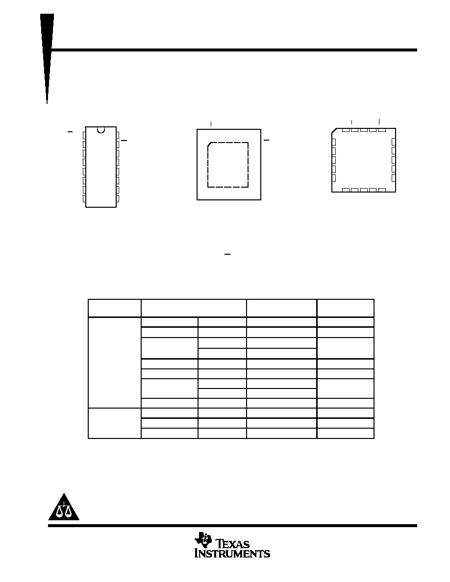
SN54AHC157 . . . J OR W PACKAGE
SN74AHC157 . . . D, DB, DGV, N, NS,
OR PW PACKAGE
(TOP VIEW)
3
2 1 20 19
9 10 11 12 13
4
5
6
7
8
18
17
16
15
14
4A
4B
NC
4Y
3A
1B
1Y
NC
2A
2B
SN54AHC157 . . . FK PACKAGE
(TOP VIEW)
1A
A/B
NC
3Y
3B
V
G
2Y
GND
NC
CC
1
2
3
4
5
6
7
8
16
15
14
13
12
11
10
9
A /B
1A
1B
1Y
2A
2B
2Y
GND
V
CC
G
4A
4B
4Y
3A
3B
3Y
NC No internal connection
SN74AHC157 . . . RGY PACKAGE
(TOP VIEW)
1
16
8
9
2
3
4
5
6
7
15
14
13
12
11
10
G
4A
4B
4Y
3A
3B
1A
1B
1Y
2A
2B
2Y
A/B
3Y
V
GND
CC
description/ordering information
These quadruple 2-line to 1-line data selectors/multiplexers are designed for 2-V to 5.5-V V
CC
operation.
The 'AHC157 devices feature a common strobe (G) input. When the strobe is high, all outputs are low. When
the strobe is low, a 4-bit word is selected from one of two sources and is routed to the four outputs. The devices
provide true data.
ORDERING INFORMATION
TA
PACKAGE
ORDERABLE
PART NUMBER
TOP-SIDE
MARKING
QFN RGY
Tape and reel
SN74AHC157RGYR
HA157
PDIP N
Tube
SN74AHC157N
SN74AHC157N
SOIC D
Tube
SN74AHC157D
AHC157
SOIC D
Tape and reel
SN74AHC157DR
AHC157
40
°
C to 85
°
C
SOP NS
Tape and reel
SN74AHC157NSR
AHC157
SSOP DB
Tape and reel
SN74AHC157DBR
HA157
TSSOP
PW
Tube
SN74AHC157PW
HA157
TSSOP PW
Tape and reel
SN74AHC157PWR
HA157
TVSOP DGV
Tape and reel
SN74AHC157DGVR
HA157
CDIP J
Tube
SNJ54AHC157J
SNJ54AHC157J
55
°
C to 125
°
C
CFP W
Tube
SNJ54AHC157W
SNJ54AHC157W
LCCC FK
Tube
SNJ54AHC157FK
SNJ54AHC157FK
Package drawings, standard packing quantities, thermal data, symbolization, and PCB design guidelines
are available at www.ti.com/sc/package.
Copyright
2003, Texas Instruments Incorporated
PRODUCTION DATA information is current as of publication date.
Products conform to specifications per the terms of Texas Instruments
standard warranty. Production processing does not necessarily include
testing of all parameters.
Please be aware that an important notice concerning availability, standard warranty, and use in critical applications of
Texas Instruments semiconductor products and disclaimers thereto appears at the end of this data sheet.
On products compliant to MIL-PRF-38535, all parameters are tested
unless otherwise noted. On all other products, production
processing does not necessarily include testing of all parameters.
SN54AHC157, SN74AHC157
QUADRUPLE 2-LINE TO 1-LINE DATA SELECTORS/MULTIPLEXERS
SCLS345I MAY 1996 REVISED JULY 2003
2
POST OFFICE BOX 655303
·
DALLAS, TEXAS 75265
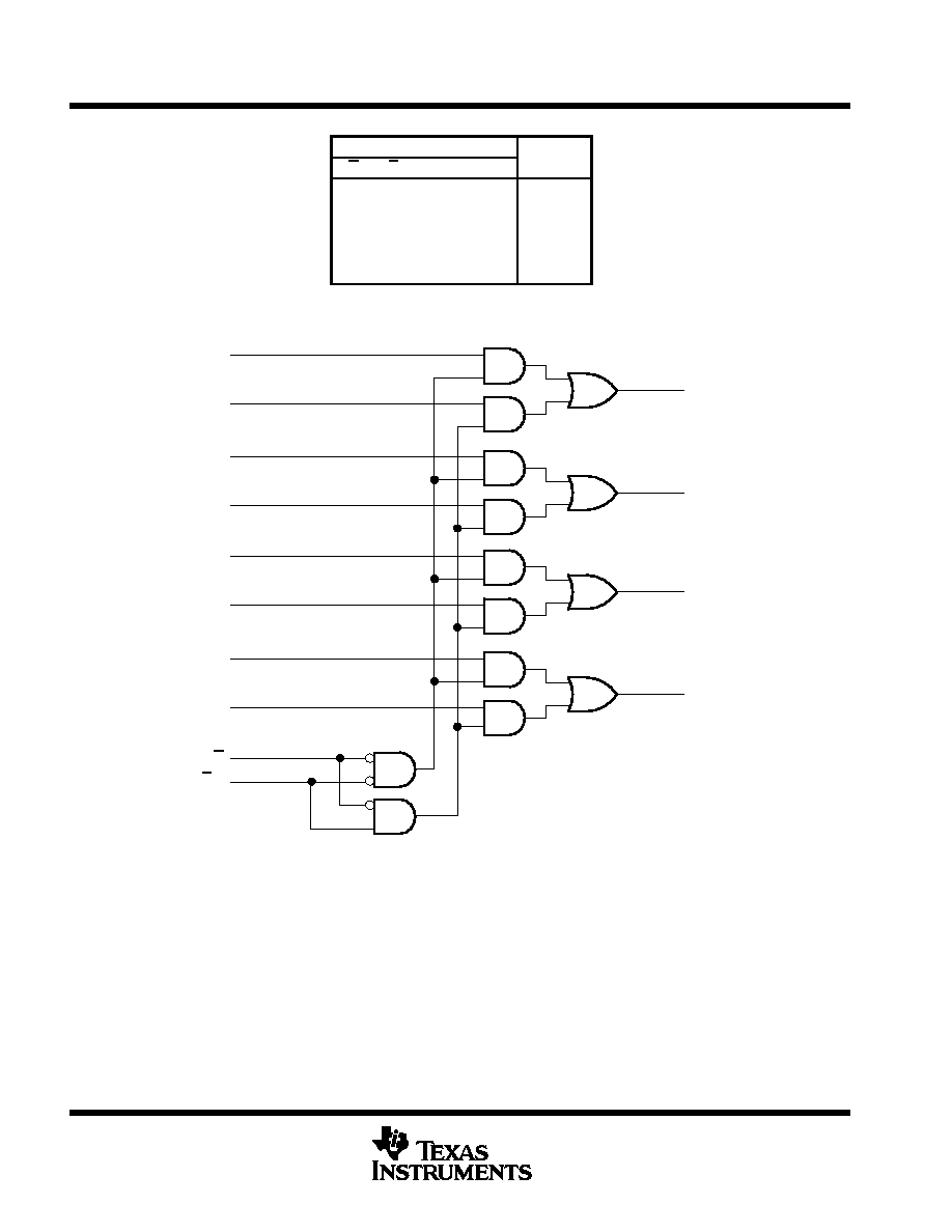
FUNCTION TABLE
INPUTS
OUTPUT
G
A/B
A
B
Y
H
X
X
X
L
L
L
L
X
L
L
L
H
X
H
L
H
X
L
L
L
H
X
H
H
logic diagram (positive logic)
2
3
5
6
11
10
14
13
15
1
G
A/B
4B
4A
3B
3A
2B
2A
1B
1A
4
7
9
12
1Y
2Y
3Y
4Y
Pin numbers shown are for the D, DB, DGV, J, N, NS, PW, RGY, and W packages.
SN54AHC157, SN74AHC157
QUADRUPLE 2-LINE TO 1-LINE DATA SELECTORS/MULTIPLEXERS
SCLS345I MAY 1996 REVISED JULY 2003
3
POST OFFICE BOX 655303
·
DALLAS, TEXAS 75265
absolute maximum ratings over operating free-air temperature range (unless otherwise noted)
Supply voltage range, V
CC
0.5 V to 7 V
. . . . . . . . . . . . . . . . . . . . . . . . . . . . . . . . . . . . . . . . . . . . . . . . . . . . . . . . . .
Input voltage range, V
I
(see Note 1)
0.5 V to 7 V
. . . . . . . . . . . . . . . . . . . . . . . . . . . . . . . . . . . . . . . . . . . . . . . . . .
Output voltage range, V
O
(see Note 1)
0.5 V to V
CC
+ 0.5 V
. . . . . . . . . . . . . . . . . . . . . . . . . . . . . . . . . . . . . . . .
Input clamp current, I
IK
(V
I
< 0)
20 mA
. . . . . . . . . . . . . . . . . . . . . . . . . . . . . . . . . . . . . . . . . . . . . . . . . . . . . . . . . . .
Output clamp current, I
OK
(V
O
< 0 or V
O
> V
CC
)
±
20 mA
. . . . . . . . . . . . . . . . . . . . . . . . . . . . . . . . . . . . . . . . . . . .
Continuous output current, I
O
(V
O
= 0 to V
CC
)
±
25 mA
. . . . . . . . . . . . . . . . . . . . . . . . . . . . . . . . . . . . . . . . . . . . . .
Continuous current through V
CC
or GND
±
50 mA
. . . . . . . . . . . . . . . . . . . . . . . . . . . . . . . . . . . . . . . . . . . . . . . . . . .
Package thermal impedance,
JA
(see Note 2): D package
73
°
C/W
. . . . . . . . . . . . . . . . . . . . . . . . . . . . . . . . . . .
(see Note 2): DB package
82
°
C/W
. . . . . . . . . . . . . . . . . . . . . . . . . . . . . . . . .
(see Note 2): DGV package
120
°
C/W
. . . . . . . . . . . . . . . . . . . . . . . . . . . . . . .
(see Note 2): N package
67
°
C/W
. . . . . . . . . . . . . . . . . . . . . . . . . . . . . . . . . . .
(see Note 2): NS package
64
°
C/W
. . . . . . . . . . . . . . . . . . . . . . . . . . . . . . . . .
(see Note 2): PW package
108
°
C/W
. . . . . . . . . . . . . . . . . . . . . . . . . . . . . . . .
(see Note 3): RGY package
39
°
C/W
. . . . . . . . . . . . . . . . . . . . . . . . . . . . . . . .
Storage temperature range, T
stg
65
°
C to 150
°
C
. . . . . . . . . . . . . . . . . . . . . . . . . . . . . . . . . . . . . . . . . . . . . . . . . . .
Stresses beyond those listed under "absolute maximum ratings" may cause permanent damage to the device. These are stress ratings only, and
functional operation of the device at these or any other conditions beyond those indicated under "recommended operating conditions" is not
implied. Exposure to absolute-maximum-rated conditions for extended periods may affect device reliability.
NOTES:
1. The input and output voltage ratings may be exceeded if the input and output current ratings are observed.
2. The package thermal impedance is calculated in accordance with JESD 51-7.
3. The package thermal impedance is calculated in accordance with JESD 51-5.
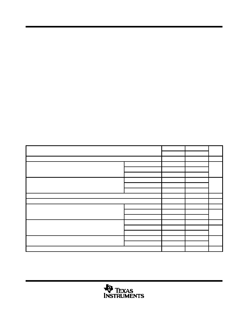
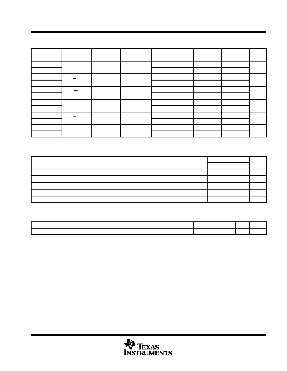
recommended operating conditions (see Note 4)
SN54AHC157
SN74AHC157
UNIT
MIN
MAX
MIN
MAX
UNIT
VCC
Supply voltage
2
5.5
2
5.5
V
VCC = 2 V
1.5
1.5
VIH
High-level input voltage
VCC = 3 V
2.1
2.1
V
VCC = 5.5 V
3.85
3.85
VCC = 2 V
0.5
0.5
VIL
Low-level input voltage
VCC = 3 V
0.9
0.9
V
VCC = 5.5 V
1.65
1.65
VI
Input voltage
0
5.5
0
5.5
V
VO
Output voltage
0
VCC
0
VCC
V
VCC = 2 V
50
50
m
A
IOH
High-level output current
VCC = 3.3 V
±
0.3 V
4
4
mA
VCC = 5 V
±
0.5 V
8
8
mA
VCC = 2 V
50
50
m
A
IOL
Low-level output current
VCC = 3.3 V
±
0.3 V
4
4
mA
VCC = 5 V
±
0.5 V
8
8
mA
t/
v
Input transition rise or fall rate
VCC = 3.3 V
±
0.3 V
100
100
ns/V
t/
v
Input transition rise or fall rate
VCC = 5 V
±
0.5 V
20
20
ns/V
TA
Operating free-air temperature
55
125
40
85
°
C
NOTE 4: All unused inputs of the device must be held at VCC or GND to ensure proper device operation. Refer to the TI application report,
Implications of Slow or Floating CMOS Inputs, literature number SCBA004.
SN54AHC157, SN74AHC157
QUADRUPLE 2-LINE TO 1-LINE DATA SELECTORS/MULTIPLEXERS
SCLS345I MAY 1996 REVISED JULY 2003
4
POST OFFICE BOX 655303
·
DALLAS, TEXAS 75265
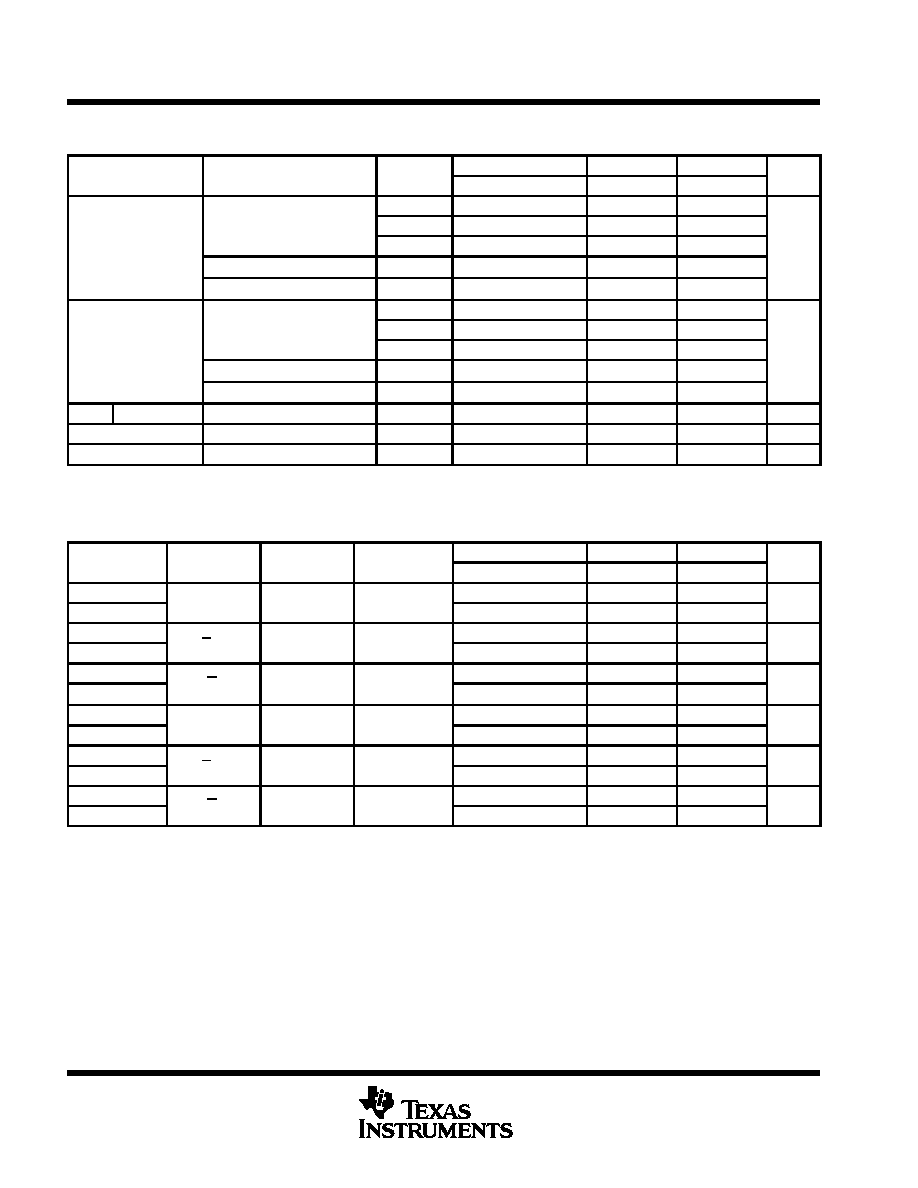
electrical characteristics over recommended operating free-air temperature range (unless
otherwise noted)
PARAMETER
TEST CONDITIONS
VCC
TA = 25
°
C
SN54AHC157
SN74AHC157
UNIT
PARAMETER
TEST CONDITIONS
VCC
MIN
TYP
MAX
MIN
MAX
MIN
MAX
UNIT
2 V
1.9
2
1.9
1.9
IOH = 50
m
A
3 V
2.9
3
2.9
2.9
VOH
4.5 V
4.4
4.5
4.4
4.4
V
OH
IOH = 4 mA
3 V
2.58
2.48
2.48
IOH = 8 mA
4.5 V
3.94
3.8
3.8
2 V
0.1
0.1
0.1
IOL = 50
m
A
3 V
0.1
0.1
0.1
VOL
4.5 V
0.1
0.1
0.1
V
OL
IOL = 4 mA
3 V
0.36
0.5
0.44
IOL = 8 mA
4.5 V
0.36
0.5
0.44
II
A or B inputs
VI = 5.5 V or GND
0 V to 5.5 V
±
0.1
±
1*
±
1
m
A
ICC
VI = VCC or GND,
IO = 0
5.5 V
4
40
40
m
A
Ci
VI = VCC or GND
5 V
2
10
10
pF
* On products compliant to MIL-PRF-38535, this parameter is not production tested at VCC = 0 V.
switching characteristics over recommended operating free-air temperature range,
V
CC
= 3.3 V
±
0.3 V (unless otherwise noted) (see Figure 1)
PARAMETER
FROM
TO
LOAD
TA = 25
°
C
SN54AHC157
SN74AHC157
UNIT
PARAMETER
(INPUT)
(OUTPUT)
CAPACITANCE
MIN
TYP
MAX
MIN
MAX
MIN
MAX
UNIT
tPLH
A or B
Y
CL = 15 pF
6.2**
9.7**
1**
11.5**
1
11.5
ns
tPHL
A or B
Y
CL = 15 pF
6.2**
9.7**
1**
11.5**
1
11.5
ns
tPLH
A/B
Y
CL = 15 pF
8.4**
13.2**
1**
15.5**
1
15.5
ns
tPHL
A/B
Y
CL = 15 pF
8.4**
13.2**
1**
15.5**
1
15.5
ns
tPLH
G
Y
CL = 15 pF
8.7**
13.6**
1**
16**
1
16
ns
tPHL
G
Y
CL = 15 pF
8.7**
13.6**
1**
16**
1
16
ns
tPLH
A or B
Y
CL = 50 pF
8.7
13.2
1
15
1
15
ns
tPHL
A or B
Y
CL = 50 pF
8.7
13.2
1
15
1
15
ns
tPLH
A/B
Y
CL = 50 pF
10.9
16.7
1
19
1
19
ns
tPHL
A/B
Y
CL = 50 pF
10.9
16.7
1
19
1
19
ns
tPLH
G
Y
CL = 50 pF
11.2
17.1
1
19.5
1
19.5
ns
tPHL
G
Y
CL = 50 pF
11.2
17.1
1
19.5
1
19.5
ns
** On products compliant to MIL-PRF-38535, this parameter is not production tested.
SN54AHC157, SN74AHC157
QUADRUPLE 2-LINE TO 1-LINE DATA SELECTORS/MULTIPLEXERS
SCLS345I MAY 1996 REVISED JULY 2003
5
POST OFFICE BOX 655303
·
DALLAS, TEXAS 75265
switching characteristics over recommended operating free-air temperature range,
V
CC
= 5 V
±
0.5 V (unless otherwise noted) (see Figure 1)
PARAMETER
FROM
TO
LOAD
TA = 25
°
C
SN54AHC157
SN74AHC157
UNIT
PARAMETER
(INPUT)
(OUTPUT)
CAPACITANCE
MIN
TYP
MAX
MIN
MAX
MIN
MAX
UNIT
tPLH
A or B
Y
CL = 15 pF
4.1*
6.4*
1*
7.5*
1
7.5
ns
tPHL
A or B
Y
CL = 15 pF
4.1*
6.4*
1*
7.5*
1
7.5
ns
tPLH
A/B
Y
CL = 15 pF
5.3*
8.1*
1*
9.5*
1
9.5
ns
tPHL
A/B
Y
CL = 15 pF
5.3*
8.1*
1*
9.5*
1
9.5
ns
tPLH
G
Y
CL = 15 pF
5.6*
8.6*
1*
10*
1
10
ns
tPHL
G
Y
CL = 15 pF
5.6*
8.6*
1*
10*
1
10
ns
tPLH
A or B
Y
CL = 50 pF
5.6
8.4
1
9.5
1
9.5
ns
tPHL
A or B
Y
CL = 50 pF
5.6
8.4
1
9.5
1
9.5
ns
tPLH
A/B
Y
CL = 50 pF
6.8
10.1
1
11.5
1
11.5
ns
tPLH
A/B
Y
CL = 50 pF
6.8
10.1
1
11.5
1
11.5
ns
tPLH
G
Y
CL = 50 pF
7.1
10.6
1
12
1
12
ns
tPHL
G
Y
CL = 50 pF
7.1
10.6
1
12
1
12
ns
* On products compliant to MIL-PRF-38535, this parameter is not production tested.
noise characteristics V
CC
= 5 V, C
L
= 50 pF, T
A
= 25
°
C (see Note 5)
PARAMETER
SN74AHC157
UNIT
PARAMETER
MIN
TYP
MAX
UNIT
VOL(P)
Quiet output, maximum dynamic VOL
0.8
V
VOL(V)
Quiet output, minimum dynamic VOL
0.8
V
VOH(V)
Quiet output, minimum dynamic VOH
4.8
V
VIH(D)
High-level dynamic input voltage
3.5
V
VIL(D)
Low-level dynamic input voltage
1.5
V
NOTE 5: Characteristics are for surface-mount packages only.
operating characteristics, V
CC
= 5 V, T
A
= 25
°
C
PARAMETER
TEST CONDITIONS
TYP
UNIT
Cpd
Power dissipation capacitance
No load,
f = 1 MHz
11
pF