SN54AHC123A, SN74AHC123A
DUAL RETRIGGERABLE MONOSTABLE MULTIVIBRATORS
SCLS352G ≠ JULY 1997 ≠ REVISED APRIL 2003
1
POST OFFICE BOX 655303
∑
DALLAS, TEXAS 75265
D
Operating Range 2-V to 5.5-V V
CC
D
Schmitt-Trigger Circuitry On A, B, and CLR
Inputs for Slow Input Transition Rates
D
Edge Triggered From Active-High or
Active-Low Gated Logic Inputs
D
Retriggerable for Very Long Output Pulses
D
Overriding Clear Terminates Output Pulse
D
Glitch-Free Power-Up Reset On Outputs
D
Latch-Up Performance Exceeds 100 mA Per
JESD 78, Class II
D
ESD Protection Exceeds JESD 22
≠ 2000-V Human-Body Model (A114-A)
≠ 200-V Machine Model (A115-A)
≠ 1000-V Charged-Device Model (C101)
description/ordering information
The 'AHC123A devices are dual retriggerable
monostable multivibrators designed for 2-V to
5.5-V V
CC
operation.
These edge-triggered multivibrators feature
output pulse-duration control by three methods. In
the first method, the A input is low, and the B input
goes high. In the second method, the B input is
high, and the A input goes low. In the third method,
the A input is low, the B input is high, and the clear
(CLR) input goes high.
ORDERING INFORMATION
TA
PACKAGE
ORDERABLE
PART NUMBER
TOP-SIDE
MARKING
PDIP ≠ N
Tube
SN74AHC123AN
SN74AHC123AN
SOIC
D
Tube
SN74AHC123AD
AHC123A
40
∞
C to 85
∞
C
SOIC ≠ D
Tape and reel
SN74AHC123ADR
AHC123A
≠40
∞
C to 85
∞
C
SSOP ≠ DB
Tape and reel
SN74AHC123ADBR
HA123A
TSSOP ≠ PW
Tape and reel
SN74AHC123APWR
HA123A
TVSOP ≠ DGV
Tape and reel
SN74AHC123ADGVR
HA123A
CDIP ≠ J
Tube
SNJ54AHC123AJ
SNJ54AHC123AJ
≠55
∞
C to 125
∞
C
CFP ≠ W
Tube
SNJ54AHC123AW
SNJ54AHC123AW
LCCC ≠ FK
Tube
SNJ54AHC123AFK
SNJ54AHC123AFK
Package drawings, standard packing quantities, thermal data, symbolization, and PCB design guidelines are
available at www.ti.com/sc/package.
Copyright
2003, Texas Instruments Incorporated
Please be aware that an important notice concerning availability, standard warranty, and use in critical applications of
Texas Instruments semiconductor products and disclaimers thereto appears at the end of this data sheet.
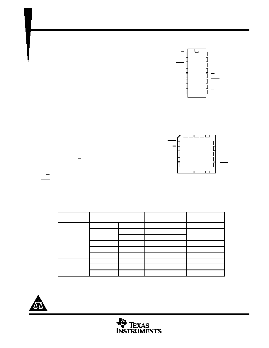
SN54AHC123A . . . J OR W PACKAGE
SN74AHC123A . . . D, DB, DGV, N, OR PW PACKAGE
(TOP VIEW)
SN54AHC123A . . . FK PACKAGE
(TOP VIEW)
1
2
3
4
5
6
7
8
16
15
14
13
12
11
10
9
1A
1B
1CLR
1Q
2Q
2C
ext
2R
ext
/C
ext
GND
V
CC
1R
ext
/C
ext
1C
ext
1Q
2Q
2CLR
2B
2A
3
2
1 20 19
9 10 11 12 13
4
5
6
7
8
18
17
16
15
14
1C
ext
1Q
NC
2Q
2CLR
1CLR
1Q
NC
2Q
2C
ext
1B
1A
NC
2A
2B
V
1R
2R
GND
NC
CC
NC ≠ No internal connection
ext
/C
ext
ext
/C
ext
PRODUCTION DATA information is current as of publication date.
Products conform to specifications per the terms of Texas Instruments
standard warranty. Production processing does not necessarily include
testing of all parameters.
On products compliant to MIL-PRF-38535, all parameters are tested
unless otherwise noted. On all other products, production
processing does not necessarily include testing of all parameters.

SN54AHC123A, SN74AHC123A
DUAL RETRIGGERABLE MONOSTABLE MULTIVIBRATORS
SCLS352G ≠ JULY 1997 ≠ REVISED APRIL 2003
2
POST OFFICE BOX 655303
∑
DALLAS, TEXAS 75265
description/ordering information (continued)
The output pulse duration is programmed by selecting external resistance and capacitance values. The external
timing capacitor must be connected between C
ext
and R
ext
/C
ext
(positive) and an external resistor connected
between R
ext
/C
ext
and V
CC
. To obtain variable pulse durations, connect an external variable resistance between
R
ext
/C
ext
and V
CC
. The output pulse duration also can be reduced by taking CLR low.
Pulse triggering occurs at a particular voltage level and is not directly related to the transition time of the input
pulse. The A, B, and CLR inputs have Schmitt triggers with sufficient hysteresis to handle slow input transition
rates with jitter-free triggering at the outputs.
Once triggered, the basic pulse duration can be extended by retriggering the gated low-level-active (A) or
high-level-active (B) input. Pulse duration can be reduced by taking CLR low. CLR input can be used to override
A or B inputs. The input/output timing diagram illustrates pulse control by retriggering the inputs and early
clearing.
The variance in output pulse duration from device to device typically is less than
±
0.5% for given external timing
components. An example of this distribution for the 'AHC123A is shown in Figure 10. Variations in output pulse
duration versus supply voltage and temperature are shown in Figure 6.
During power up, Q outputs are in the low state, and Q outputs are in the high state. The outputs are glitch free,
without applying a reset pulse.
For additional application information on multivibrators, see the application report Designing With the
SN74AHC123A and SN74AHCT123A, literature number SCLA014.
FUNCTION TABLE
(each multivibrator)
INPUTS
OUTPUTS
CLR
A
B
Q
Q
L
X
X
L
H
X
H
X
L
H
X
X
L
L
H
H
L
H
#
H
L
H
These outputs are based on the
assumption that the indicated
steady-state conditions at the A and
B inputs have been set up long enough to
complete any pulse started before the
setup.

SN54AHC123A, SN74AHC123A
DUAL RETRIGGERABLE MONOSTABLE MULTIVIBRATORS
SCLS352G ≠ JULY 1997 ≠ REVISED APRIL 2003
3
POST OFFICE BOX 655303
∑
DALLAS, TEXAS 75265
logic diagram, each multivibrator (positive logic)
CLR
Cext
Rext/Cext
R
B
A
Q
Q
input/output timing diagram
A
B
CLR
Q
Q
tw
tw
tw + trr
trr
Rext/Cext

SN54AHC123A, SN74AHC123A
DUAL RETRIGGERABLE MONOSTABLE MULTIVIBRATORS
SCLS352G ≠ JULY 1997 ≠ REVISED APRIL 2003
4
POST OFFICE BOX 655303
∑
DALLAS, TEXAS 75265
absolute maximum ratings over operating free-air temperature (unless otherwise noted)
Supply voltage range, V
CC
(see Note 1)
≠0.5 V to 7 V
. . . . . . . . . . . . . . . . . . . . . . . . . . . . . . . . . . . . . . . . . . . . . .
Input voltage range, V
I
(see Note 2)
≠0.5 V to 7 V
. . . . . . . . . . . . . . . . . . . . . . . . . . . . . . . . . . . . . . . . . . . . . . . . . .
Output voltage range in high or low state, V
O
(see Note 1)
≠0.5 V to V
CC
+ 0.5 V
. . . . . . . . . . . . . . . . . . . . . . .
Output voltage range in power-off state, V
O
(see Note 1)
≠0.5 V to 7 V
. . . . . . . . . . . . . . . . . . . . . . . . . . . . . . . .
Input clamp current, I
IK
(V
I
< 0)
≠20 mA
. . . . . . . . . . . . . . . . . . . . . . . . . . . . . . . . . . . . . . . . . . . . . . . . . . . . . . . . . . .
Output clamp current, I
OK
(V
O
< 0 or V
O
> V
CC
)
±
20 mA
. . . . . . . . . . . . . . . . . . . . . . . . . . . . . . . . . . . . . . . . . . . .
Continuous output current, I
O
(V
O
= 0 to V
CC
)
±
25 mA
. . . . . . . . . . . . . . . . . . . . . . . . . . . . . . . . . . . . . . . . . . . . . .
Continuous current through V
CC
or GND
±
50 mA
. . . . . . . . . . . . . . . . . . . . . . . . . . . . . . . . . . . . . . . . . . . . . . . . . . .
Package thermal impedance,
JA
(see Note 3): D package
73
∞
C/W
. . . . . . . . . . . . . . . . . . . . . . . . . . . . . . . . . . .
DB package
82
∞
C/W
. . . . . . . . . . . . . . . . . . . . . . . . . . . . . . . . .
DGV package
120
∞
C/W
. . . . . . . . . . . . . . . . . . . . . . . . . . . . . . .
N package
67
∞
C/W
. . . . . . . . . . . . . . . . . . . . . . . . . . . . . . . . . . .
PW package
108
∞
C/W
. . . . . . . . . . . . . . . . . . . . . . . . . . . . . . . .
Storage temperature range, T
stg
≠65
∞
C to 150
∞
C
. . . . . . . . . . . . . . . . . . . . . . . . . . . . . . . . . . . . . . . . . . . . . . . . . . .
Stresses beyond those listed under "absolute maximum ratings" may cause permanent damage to the device. These are stress ratings only, and
functional operation of the device at these or any other conditions beyond those indicated under "recommended operating conditions" is not
implied. Exposure to absolute-maximum-rated conditions for extended periods may affect device reliability.
NOTES:
1. Voltage values are with respect to the network ground terminal.
2. The input and output voltage ratings may be exceeded if the input and output current ratings are observed.
3. The package thermal impedance is calculated in accordance with JESD 51-7.
recommended operating conditions (see Note 4)
SN54AHC123A
SN74AHC123A
UNIT
MIN
MAX
MIN
MAX
UNIT
VCC
Supply voltage
2
5.5
2
5.5
V
VCC = 2 V
1.5
1.5
VIH
High-level input voltage
VCC = 3 V
2.1
2.1
V
VCC = 5.5 V
3.85
3.85
VCC = 2 V
0.5
0.5
VIL
Low-level input voltage
VCC = 3 V
0.9
0.9
V
VCC = 5.5 V
1.65
1.65
VI
Input voltage
0
5.5
0
5.5
V
VO
Output voltage
0
VCC
0
VCC
V
VCC = 2 V
≠50
≠50
m
A
IOH
High-level output current
VCC = 3.3 V
±
0.3 V
≠4
≠4
mA
VCC = 5 V
±
0.5 V
≠8
≠8
mA
VCC = 2 V
50
50
m
A
IOL
Low-level output current
VCC = 3.3 V
±
0.3 V
4
4
mA
VCC = 5 V
±
0.5 V
8
8
mA
R
t
External timing resistance
VCC = 2 V
5k
5k
Rext
External timing resistance
VCC > 3 V
1k
1k
t/
VCC
Power-up ramp rate
1
1
ms/V
TA
Operating free-air temperature
≠55
125
≠40
85
∞
C
NOTE 4: Unused Rext/Cext terminals should be left unconnected. All remaining unused inputs of the device must be held at VCC or GND to ensure
proper device operation. Refer to the TI application report, Implications of Slow or Floating CMOS Inputs, literature number SCBA004.

SN54AHC123A, SN74AHC123A
DUAL RETRIGGERABLE MONOSTABLE MULTIVIBRATORS
SCLS352G ≠ JULY 1997 ≠ REVISED APRIL 2003
5
POST OFFICE BOX 655303
∑
DALLAS, TEXAS 75265
electrical characteristics over recommended operating free-air temperature range (unless
otherwise noted)
PARAMETER
TEST CONDITIONS
VCC
TA = 25
∞
C
SN54AHC123A
SN74AHC123A
UNIT
PARAMETER
TEST CONDITIONS
VCC
MIN
TYP
MAX
MIN
MAX
MIN
MAX
UNIT
2 V
1.9
2
1.9
1.9
IOH = ≠50
m
A
3 V
2.9
3
2.9
2.9
VOH
4.5 V
4.4
4.5
4.4
4.4
V
IOH = ≠4 mA
3 V
2.58
2.48
2.48
IOH = ≠8 mA
4.5 V
3.94
3.8
3.8
2 V
0.1
0.1
0.1
IOL = 50
m
A
3 V
0.1
0.1
0.1
VOL
4.5 V
0.1
0.1
0.1
V
IOL = 4 mA
3 V
0.36
0.5
0.44
IOL = 8 mA
4.5 V
0.36
0.5
0.44
II
Rext/Cext
VI = VCC or GND
5.5 V
±
0.25
±
2.5
±
2.5
m
A
II
A, B, and CLR
VI = VCC or GND
0 V to 5.5 V
±
0.1
±
1*
±
1
m
A
ICC
Quiescent
VI = VCC or GND, IO = 0
5.5 V
4
40
40
m
A
A ti
t t
V
V
GND
3 V
160
250
280
280
ICC
Active state
(per circuit)
VI = VCC or GND,
Rext/Cext = 0 5 VCC
4.5 V
280
500
650
650
m
A
( er circuit)
Rext/Cext = 0.5 VCC
5.5 V
360
750
975
975
Ci
VI = VCC or GND
5 V
1.9
10
10
pF
* On products compliant to MIL-PRF-38535, this parameter is not production tested at VCC = 0 V.
This test is performed with the terminal in the off-state condition.
timing requirements over recommended operating free-air temperature range, V
CC
= 3.3 V
±
0.3 V
(unless otherwise noted) (see Figure 1)
TEST CONDITIONS
TA = 25
∞
C
SN54AHC123A
SN74AHC123A
UNIT
TEST CONDITIONS
MIN
TYP
MAX
MIN
MAX
MIN
MAX
UNIT
t
Pulse
CLR
5
5
5
ns
tw
duration
A or B trigger
5
5
5
ns
t
Pulse retrigger time
Rext = 1 k
, Cext = 100 pF
76
ns
trr
Pulse retrigger time
Rext = 1 k
, Cext = 0.01
m
F
1.8
m
s
See retriggering data in the application information section.
timing requirements over recommended operating free-air temperature range, V
CC
= 5 V
±
0.5 V
(unless otherwise noted) (see Figure 1)
TEST CONDITIONS
TA = 25
∞
C
SN54AHC123A
SN74AHC123A
UNIT
TEST CONDITIONS
MIN
TYP
MAX
MIN
MAX
MIN
MAX
UNIT
t
Pulse
CLR
5
5
5
ns
tw
duration
A or B trigger
5
5
5
ns
t
Pulse retrigger time
Rext = 1 k
, Cext = 100 pF
59
ns
trr
Pulse retrigger time
Rext = 1 k
, Cext = 0.01
m
F
1.5
m
s
See retriggering data in the application information section.