SMJ320F240 DSP Controller (Rev. B)

Please be aware that an important notice concerning availability, standard warranty, and use in critical applications of
Texas Instruments semiconductor products and disclaimers thereto appears at the end of this data sheet.
SMJ320F240
DSP CONTROLLER
SGUS029B APRIL 1999 REVISED JULY 2003
1
POST OFFICE BOX 1443
·
HOUSTON, TEXAS 772511443
D
Processed to MIL-PRF-38535 (QML)
D
High-Performance Static CMOS Technology
D
Includes the T320C2xLP Core CPU
Object Compatible With the TMS320C2xx
Family
Source Code Compatible With
SMJ320C25
Upwardly Compatible With SMJ320C50
50-ns Instruction Cycle Time
D
Memory
544 Words
×
16 Bits of On-Chip
Data/Program Dual-Access RAM
16K Words
×
16 Bits of On-Chip Program
Flash EEPROM
224K Words
×
16 Bits of Total Memory
Address Reach (64K Data, 64K Program
and 64K I/O, and 32K Global Memory
Space)
D
Event-Manager Module
12 Compare/Pulse-Width Modulation
(PWM) Channels
Three 16-Bit General-Purpose Timers
With Six Modes, Including Continuous
Upand Up/Down Counting
Three 16-Bit Full-Compare Units With
Deadband
Three 16-Bit Simple-Compare Units
Four Capture Units (Two With
Quadrature Encoder-Pulse Interface
Capability)
D
Dual 10-Bit Analog-to-Digital Conversion
Module
D
28 Individually Programmable, Multiplexed
I/O Pins
D
Phase-Locked-Loop (PLL)-Based Clock
Module
D
Watchdog Timer Module (With Real-Time
Interrupt)
D
Serial Communications Interface (SCI)
Module
D
Serial Peripheral Interface (SPI) Module
D
Six External Interrupts (Power Drive
Protect, Reset, NMI, and Three Maskable
Interrupts)
D
Four Power-Down Modes for Low-Power
Operation
D
Scan-Based Emulation
D
Development Tools Available:
Texas Instruments (TI
) ANSI
C Compiler, Assembler/Linker, and
C-Source Debugger
Scan-Based Self-Emulation (XDS510
)
Third-Party Digital Motor Control and
Fuzzy-Logic Development Support
D
55
°
C to 125
°
C Operating Temperature
Range, QML Processing
D
132-Pin Ceramic Quad Flat Package
(HFP Suffix)
description
The SMJ320F240 is the first member of a new family of digital signal processor (DSP) controllers based on the
TMS320C2xx generation of 16-bit fixed-point DSPs. This new family is optimized for digital motor/motion control
applications and contains 16K words of flash memory on chip. The DSP controller combines the enhanced
TMS320 architectural design of the 'C2xLP core CPU for low-cost, high-performance processing capabilities
and several advanced peripherals optimized for motor/motion control applications. These peripherals include
the event manager module, which provides general-purpose timers and compare registers to generate up to
12 PWM outputs, and a dual 10-bit analog-to-digital converter (ADC), which can perform two simultaneous
conversions within 6.1
µ
s.
On products compliant to MIL PRF 38535, all parameters are tested
unless otherwise noted. On all other products, production
processing does not necessarily include testing of all parameters.
Copyright
2003, Texas Instruments Incorporated
TI and XDS510 are trademarks of Texas Instruments Incorporated.
PRODUCTION DATA information is current as of publication date.
Products conform to specifications per the terms of Texas Instruments
standard warranty. Production processing does not necessarily include
testing of all parameters.
SMJ320F240
DSP CONTROLLER
SGUS029B APRIL 1999 REVISED JULY 2003
2
POST OFFICE BOX 1443
·
HOUSTON, TEXAS 772511443
Table of Contents
Description
1
. . . . . . . . . . . . . . . . . . . . . . . . . . . . . . . . . . . . . . . . . . . .
Pinout
3
. . . . . . . . . . . . . . . . . . . . . . . . . . . . . . . . . . . . . . . . . . . . . . . .
Terminal Functions Table
4
. . . . . . . . . . . . . . . . . . . . . . . . . . . . . . . .
Functional Block Diagram
10
. . . . . . . . . . . . . . . . . . . . . . . . . . . . .
Device Memory Map
11
. . . . . . . . . . . . . . . . . . . . . . . . . . . . . . . . . . .
Device Reset and Interrupts
16
. . . . . . . . . . . . . . . . . . . . . . . . . . .
Clock Generation
25
. . . . . . . . . . . . . . . . . . . . . . . . . . . . . . . . . . . . .
Low-Power Modes
27
. . . . . . . . . . . . . . . . . . . . . . . . . . . . . . . . . . . .
Functional Block Diagram of the CPU
30
. . . . . . . . . . . . . . . . . . .
DSP Core CPU
31
. . . . . . . . . . . . . . . . . . . . . . . . . . . . . . . . . . . . . .
Internal Memory
35
. . . . . . . . . . . . . . . . . . . . . . . . . . . . . . . . . . . . . .
Peripherals
37
. . . . . . . . . . . . . . . . . . . . . . . . . . . . . . . . . . . . . . . . . .
Scan-based Emulation
49
. . . . . . . . . . . . . . . . . . . . . . . . . . . . . . . .
SMJ320F240 Instruction Set
49
. . . . . . . . . . . . . . . . . . . . . . . . . . .
Absolute Maximum Ratings
59
. . . . . . . . . . . . . . . . . . . . . . . . . . . .
Recommended Operating Conditions
59
. . . . . . . . . . . . . . . . . . .
Electrical Characteristics
60
. . . . . . . . . . . . . . . . . . . . . . . . . . . . . .
Signal Transition Levels
61
. . . . . . . . . . . . . . . . . . . . . . . . . . . . . . .
Clock Options
64
. . . . . . . . . . . . . . . . . . . . . . . . . . . . . . . . . . . . . . . .
Memory and Peripheral Interface Timing
68
. . . . . . . . . . . . . . . . .
I/O Timing Variation: SPICE Simulation Results
72
. . . . . . . . . . .
READY Timings
73
. . . . . . . . . . . . . . . . . . . . . . . . . . . . . . . . . . . . . .
RS and PORESET Timings
74
. . . . . . . . . . . . . . . . . . . . . . . . . . . .
XF, BIO, and MP/MC Timings
76
. . . . . . . . . . . . . . . . . . . . . . . . . .
Timing Event Manager Interface
77
. . . . . . . . . . . . . . . . . . . . . . . .
PWM/CMP Timings
77
. . . . . . . . . . . . . . . . . . . . . . . . . . . . . . . . . . .
Capture and QEP Timings
78
. . . . . . . . . . . . . . . . . . . . . . . . . . . . .
Interrupt Timings
78
. . . . . . . . . . . . . . . . . . . . . . . . . . . . . . . . . . . . .
General-Purpose Input/Output Timings
79
. . . . . . . . . . . . . . . . . .
Serial Communications Interface (SCI) I/O Timings
80
. . . . . . . .
Timing Characteristics for SCI
80
. . . . . . . . . . . . . . . . . . . . . . . . . .
SPI Master Mode Timing Parameters
81
. . . . . . . . . . . . . . . . . . . .
SPI Slave Mode Timing Parameters
85
. . . . . . . . . . . . . . . . . . . . .
10-Bit Dual Analog-to-Digital Converter (ADC)
89
. . . . . . . . . . . .
ADC Input Pin Circuit
89
. . . . . . . . . . . . . . . . . . . . . . . . . . . . . . . . .
ADC Timing Requirements
90
. . . . . . . . . . . . . . . . . . . . . . . . . . . . .
Flash EEPROM
92
. . . . . . . . . . . . . . . . . . . . . . . . . . . . . . . . . . . . . .
Programming Operation
92
. . . . . . . . . . . . . . . . . . . . . . . . . . . . . . .
Erase Operation
92
. . . . . . . . . . . . . . . . . . . . . . . . . . . . . . . . . . . . . .
Flash-write Operation
92
. . . . . . . . . . . . . . . . . . . . . . . . . . . . . . . . .
Register File Compilation
93
. . . . . . . . . . . . . . . . . . . . . . . . . . . . . .
Mechanical Data
100
. . . . . . . . . . . . . . . . . . . . . . . . . . . . . . . . . . . .
description (continued)
Table 1. Characteristics of the 'F240 DSP Controller
ON-CHIP MEMORY (WORDS)
DEVICE
RAM
FLASH
EEPROM
POWER
SUPPLY
(V)
CYCLE
TIME
(ns)
PACKAGE
TYPE
PIN COUNT
DATA
DATA/PROG
PROG
(V)
(ns)
PIN COUNT
SMJ320F240
288
256
16K
5
50
HFP 132P
The functional block diagram provides a high-level description of each component in the 'F240 DSP controller.
The SMJ320F240 device is composed of three main functional units: a 'C2xx DSP core, internal memory, and
peripherals. In addition to these three functional units, there are several system-level features of the 'F240 that
are distributed. These system features include the memory map, device reset, interrupts, digital input/output
(I/O), clock generation, and low-power operation.
SMJ320F240
DSP CONTROLLER
SGUS029B APRIL 1999 REVISED JULY 2003
3
POST OFFICE BOX 1443
·
HOUSTON, TEXAS 772511443
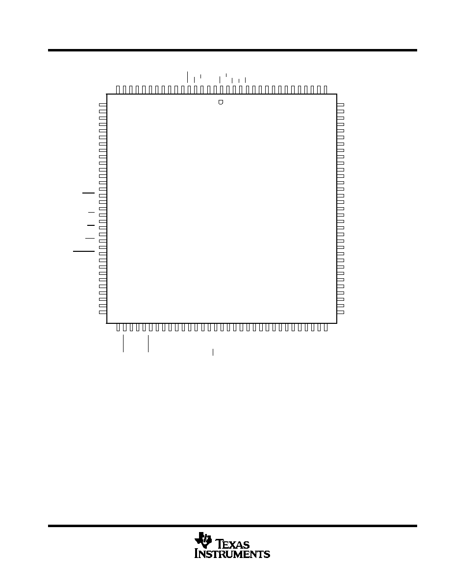
pinout
WE
W/R
D7
D8
VSS
DVDD
D9
D10
D11
D12
D13
D14
D15
VSS
TCK
TDI
TRST
TMS
TDO
RS
READY
MP/MC
EMU0
EMU1/OFF
NMI
PORESET
RESERVED
SCIRXD/IO
SCITXD/IO
SPISIMO/IO
VSS
DVDD
SPISOMI/IO
SPICLK/IO
VCCP/WDDIS
D5
D4
D3
D6
D2
STRB
BR
R/W
V
DV
PS
D1
SS
DD
A5
A4
A3
VSS
A2
A1
A0
TMRCLK/IOPB7
TMRDIR/IOPB6
T3PWM/T3CMP/IOPB5
T2PWM/T2CMP/IOPB4
T1PWM/T1CMP/IOPB3
VSS
DVDD
PWM9/CMP9/IOPB2
PWM8/CMP8/IOPB1
PWM7/CMP7/IOPB0
PWM6/CMP6
PWM5/CMP5
PWM4/CMP4
PWM3/CMP3
PWM2/CMP2
PWM1/CMP1
DVDD
VSS
ADCIN8/IOPA3
ADCIN9/IOPA2
ADCIN10
ADCIN11
VSSA
VREFLO
VREFHI
VCCA
V
SS
D0
CV
SS
CV
DD
IS
DS
A15
A14
A13
A12
A1
1
A10
A9
A8
A7
A6
V
SS
XT
AL1/CLKIN
XT
AL2
OSCBYP
XINT3/IO
XINT2/IO
XINT1
SPISTE/IO
CAP1/QEP1/IOPC4
CAP3/IOPC6
CAP4/IOPC7
CAP2/QEP2/IOPC5
BIO/IOPC3
XF/IOPC2
CLKOUT/IOPC1
ADCSOC/IOPC0
ADCIN5
ADCIN7
ADCIN15
ADCIN6
ADCIN4
ADCIN3
ADCIN1/IOP
A1
ADCIN0/IOP
A0
ADCIN14
ADCIN12
ADCIN13
ADCIN2
V
SS
V
SS
V
SS
PDPINT
DV
DD
DV
DD
DV
DD
CV
DD
132
131
130
129
128
127
126
125
124
123
122
121
120
119
118
117
116
115
114
113
112
111
110
109
108
107
106
105
104
103
102
101
100
99
98
97
96
95
94
93
92
91
90
89
88
87
86
85
84
52
51
83
82
81
80
79
78
77
76
75
74
73
72
71
70
69
68
67
66
65
64
63
62
61
60
59
58
57
56
55
54
53
50
49
48
47
46
45
44
43
42
41
40
39
38
37
36
35
34
33
32
31
30
29
28
27
26
25
24
23
22
21
20
19
18
17 16 15 14 13 12 11 10 9 8 7 6 5 4 3 2 1
SMJ320F240
DSP CONTROLLER
SGUS029B APRIL 1999 REVISED JULY 2003
4
POST OFFICE BOX 1443
·
HOUSTON, TEXAS 772511443
Terminal Functions
TERMINAL
TYPE
DESCRIPTION
NAME
NO.
TYPE
DESCRIPTION
EXTERNAL INTERFACE DATA/ADDRESS SIGNALS
A0 (LSB)
A1
A2
A3
A4
A5
A6
A7
A8
A9
A10
A11
A12
A13
A14
A15 (MSB)
110
111
112
114
115
116
117
118
119
122
123
124
125
126
127
128
O/Z
Parallel address bus A0 [least significant bit (LSB)] through A15 [most significant bit (MSB)]. A15A0 are
multiplexed to address external data/program memory or I/O. A15A0 are placed in the high-impedance
state when EMU1/OFF is active low and hold their previous states in power-down modes.
D0 (LSB)
D1
D2
D3
D4
D5
D6
D7
D8
D9
D10
D11
D12
D13
D14
D15 (MSB)
9
10
11
12
15
16
17
18
19
22
23
24
25
26
27
28
I/O/Z
Parallel data bus D0 (LSB) through D15 (MSB). D15D0 are multiplexed to transfer data between the
SMJ320F240 and external data/program memory and I/O space (devices). D15D0 are placed in the
high-impedance state when not outputting, when in power-down mode, when reset (RS) is asserted, or
when EMU1/OFF is active low.
EXTERNAL INTERFACE CONTROL SIGNALS
DS
PS
IS
129
131
130
O/Z
Data, program, and I/O space select signals. DS, PS, and IS are always high unless low-level asserted
for communication to a particular external space. They are placed in the high-impedance state during
reset, power down, and when EMU1/OFF is active low.
READY
36
I
Data ready. READY indicates that an external device is prepared for the bus transaction to be completed.
If the device is not ready (READY is low), the processor waits one cycle and checks READY again.
R/W
4
O/Z
Read/write signal. R/W indicates transfer direction during communication to an external device. It is
normally in read mode (high), unless low level is asserted for performing a write operation. It is placed
in the high-impedance state during reset, power down, and when EMU1/OFF is active low.
STRB
6
O/Z
Strobe. STRB is always high unless asserted low to indicate an external bus cycle. It is placed in the
high-impedance state during reset, power down, and when EMU1/OFF is active low.
WE
1
O/Z
Write enable. The falling edge of WE indicates that the device is driving the external data bus (D15D0).
Data can be latched by an external device on the rising edge of WE. WE is active on all external program,
data, and I/O writes. WE goes in the high-impedance state following reset and when EMU1/OFF is active
low.
W/R
132
O/Z
Write/read. W/R is an inverted form of R/W and can connect directly to the output enable of external
devices. W/R is placed in the high-impedance state following reset and when EMU1/OFF is active low.
I = input, O = output, Z = high impedance
SMJ320F240
DSP CONTROLLER
SGUS029B APRIL 1999 REVISED JULY 2003
5
POST OFFICE BOX 1443
·
HOUSTON, TEXAS 772511443
Terminal Functions (Continued)
TERMINAL
TYPE
DESCRIPTION
NAME
NO.
TYPE
DESCRIPTION
EXTERNAL INTERFACE CONTROL SIGNALS (CONTINUED)
BR
5
O/Z
Bus request. BR is asserted during access of external global data memory space. BR can be used
to extend the data memory address space by up to 32K words. BR goes in the high-impedance
state during reset, power down, and when EMU1/OFF is active low.
VCCP/WDDIS
50
I
Flash-programming voltage supply. If VCCP = 5 V, then WRITE/ERASE can be made to the
ENTIRE on-chip flash memory block--that is, for programming the flash. If VCCP = 0 V, then
WRITE/ERASE of the flash memory is not allowed, thereby protecting the entire memory block
from being overwritten. WDDIS also functions as a hardware watchdog disable. The watchdog
timer is disabled when VCCP/WDDIS = 5 V and bit 6 in WDCR is set to 1.
ADC INPUTS (UNSHARED)
ADCIN2
74
I
ADCIN3
75
I
ADCIN4
76
I
Analog inp ts to the first ADC
ADCIN5
77
I
Analog inputs to the first ADC
ADCIN6
78
I
ADCIN7
79
I
ADCIN10
89
I
ADCIN11
88
I
ADCIN12
83
I
Analog inp ts to the second ADC
ADCIN13
82
I
Analog inputs to the second ADC
ADCIN14
81
I
ADCIN15
80
I
BIT I/O AND SHARED FUNCTIONS PINS
ADCIN0/IOPA0
72
I/O
Bidirectional digital I/O.
Analog input to the first ADC.
ADCIN0/IOPA0 is configured as a digital input by all device resets.
ADCIN1/IOPA1
73
I/O
Bidirectional digital I/O.
Analog input to the first ADC.
ADCIN1/IOPA1 is configured as a digital input by all device resets.
ADCIN9/IOPA2
90
I/O
Bidirectional digital I/O.
Analog input to the second ADC.
ADCIN9/IOPA2 is configured as a digital input by all device resets.
ADCIN8/IOPA3
91
I/O
Bidirectional digital I/O.
Analog input to the second ADC.
ADCIN8/IOPA3 is configured as a digital input by all device resets.
PWM7/CMP7/IOPB0
100
I/O/Z
Bidirectional digital I/O. Simple compare/PWM 1 output. The state of PWM7/CMP7/IOPB0 is de-
termined by the simple compare/PWM and the simple action control register (SACTR). It goes to
the high-impedance state when unmasked PDPINT goes active low.
PWM7/CMP7/IOPB0 is configured as a digital input by all device resets.
PWM8/CMP8/IOPB1
101
I/O/Z
Bidirectional digital I/O. Simple compare/PWM 2 output. The state of PWM8/CMP8/IOPB1 is de-
termined by the simple compare/PWM and the SACTR. It goes to the high-impedance state when
unmasked PDPINT goes active low. PWM8/CMP8/IOPB1 is configured as a digital input by all
device resets.
PWM9/CMP9/IOPB2
102
I/O/Z
Bidirectional digital I/O. Simple compare/PWM 3 output. The state of PWM9/CMP9/IOPB2 is de-
termined by the simple compare/PWM and SACTR. It goes to the high-impedance state when un-
masked PDPINT goes active low. PWM9/CMP9/IOPB2 is configured as a digital input by all de-
vice resets.
I = input, O = output, Z = high impedance
Document Outline
- features
- description
- Table of Contents
- pinout
- Terminal Functions
- functional block diagram
- device memory map
- peripheral memory map
- digital I/O and shared pin functions
- group1 shared I/O pins
- group2 shared I/O pins
- digital I/O control registers
- device reset and interrupts
- reset
- hardware-generated interrupts
- external interrupts
- clock generation
- low-power modes
- functional block diagram of the SMJ320F240 DSP CPU
- F240 DSP core CPU
- status and control registers
- central processing unit
- input scaling shifter
- multiplier
- central arithmetic logic unit
- accumulator
- auxiliary registers and auxiliary-register arithmetic unit (ARAU)
- internal memory
- dual-access RAM (DARAM)
- flash EEPROM
- flash serial loader
- flash control mode register
- peripherals
- external memory interface
- event-manager (EV) module
- general-purpose (GP) timers
- full compare units
- programmable-deadband generator
- simple compares
- compare/ PWM waveform generation
- compare/PWMs characteristics
- capture unit
- quadrature-encoder pulse (QEP) circuit
- analog-to-digital converter (ADC) module
- serial peripheral interface (SPI) module
- serial communications interface (SCI) module
- watchdog (WD) and real-time interrupt (RTI) module
- scan-based emulation
- SMJ320F240 instruction set
- addressing modes
- repeat feature
- instruction set summary
- development support
- Software Development Tools:
- Hardware Development Tools:
- device and development-support tool nomenclature
- documentation support
- absolute maximum ratings over operating free-air temperature range (unless otherwise noted)
- recommended operating conditions
- output current variation with output voltage: SPICE simulation results (4.5 V, 150C
- electrical characteristics over recommended ranges of supply voltage and operating free-air temperature ( unless otherwise noted)
- PARAMETER MEASUREMENT INFORMATION
- signal transition levels
- timing parameter symbology
- general notes on timing parameters
- CLOCK OPTIONS
- input clock frequency over operating free-air temperature range (PLL circuit disabled)
- switching characteristics over recommended operating conditions [H = 0.5 tc(CO)]
(see Note 3 and Figure 21)
- timing requirements (see Figure 21)
- external reference crystal with PLL-circuit-enabled clock option
- input characteristics with the PLL circuit enabled
- switching characteristics over recommended operating conditions, H = 0.5 tc(CO) (see Figure 22)
- timing requirements (see Note 3 and Figure 22)
- low-power mode timings
- switching characteristics over recommended operating conditions) ( see Figure 23, Figure 24, Figure 25, and Figure 26)
- memory and parallel I/O interface read timings
- switching characteristics over recommended operating conditions for a memory read ( see Figure 27)
- timing requirements for a memory read, H = 0.5tc(CO) (see Figure 27)
- memory and parallel I/O interface write timings
- switching characteristics over recommended operating conditions for a memory write
H = 0.5tc(CO) (see Figure 28)
- I/O timing variation with load capacitance: SPICE simulation results
- READY timings
- timing requirements (see Figure 30)
- RS\ and PORESET\ timings
- switching characteristics over recommended operating conditions for a reset, H = 0.5tc(CO)
(see Figure 31, Figure 32, and Figure 33)
- timing requirements for reset (see Figure 31, Figure 32, and Figure 33)
- XF, BIO\, and MP/MC\ timings
- switching characteristics over recommended operating conditions (see Figure 34)
- timing requirements, H = 0.5tc(CO) (see Figure 34)
- PWM/CMP timings
- switching characteristics over recommended operating conditions for PWM timing (see Figure 35)
- timing requirements, [H = 0.5tc(CO)] (see Figure 36 and Figure 37)
- capture and QEP timings
- timing requirements, [H = 0.5tc(CO)] (see Figure 38)
- interrupt timings
- switching characteristics over recommended operating conditions for interrupts (see Figure 40)
- timing requirements, [H = 0.5tc(CO)] (see Figure 39 and Figure 40)
- general-purpose input/output timings
- switching characteristics over recommended operating conditions for a GPI/O (see Figure 41)
- timing requirements (see Figure 42)
- serial communications interface (SCI) I/O timings
- timing characteristics for SCI (see Note 4 and Figure 43)
- SPI master mode timing parameters
- SPI master mode external timing parameters (clock phase = 0) (see Figure 44)
- SPI master mode external timing (clock phase = 1) (see Figure 45)
- SPI slave mode timing parameters
- SPI slave mode external timing requirements (clock phase = 0) (see Figure 46)
- SPI slave mode external timing requirements (clock phase = 1) (see Figure 47)
- 10-bit dual analog-to-digital converter (ADC)
- recommended operating conditions
- electrical characteristics (see Note 5)
- ADC input pin circuit
- ADC timing requirements (see Figure 49)
- flash EEPROM
- switching characteristics over recommended operating conditions (see page 59)
- timing requirements
- programming operation (maximum programming temperature 85°C for flash memory)
- erase operation
- flash-write operation
- register file compilation
- MECHANICAL DATA
- HFP (S-GQFP-F132) CERAMIC QUAD FLATPACK
- IMPORTANT NOTICE