 | –≠–ª–µ–∫—Ç—Ä–æ–Ω–Ω—ã–π –∫–æ–º–ø–æ–Ω–µ–Ω—Ç: 7135CN | –°–∫–∞—á–∞—Ç—å:  PDF PDF  ZIP ZIP |
ICL7135C, TLC7135C
4 1/2-DIGIT PRECISION
ANALOG-TO-DIGITAL CONVERTERS
SLAS074B ≠ DECEMBER 1986 ≠ REVISED MAY 1999
1
POST OFFICE BOX 655303
∑
DALLAS, TEXAS 75265
D
Zero Reading for 0-V Input
D
Precision Null Detection With True Polarity
at Zero
D
1-pA Typical Input Current
D
True Differential Input
D
Multiplexed Binary-Coded-Decimal (BCD)
Output
D
Low Rollover Error:
±
1 Count Max
D
Control Signals Allow Interfacing With
UARTs or Microprocessors
D
Autoranging Capability With Over- and
Under-Range Signals
D
TTL-Compatible Outputs
D
Direct Replacement for Teledyne TSC7135,
Intersil ICL7135, Maxim ICL7135, and
Siliconix Si7135
D
CMOS Technology
description
The ICL7135C and TLC7135C converters are manufactured with Texas Instruments highly efficient CMOS
technology. These 4 1/2-digit, dual-slope-integrating, analog-to-digital converters (DACs) are designed to
provide interfaces to both a microprocessor and a visual display. The digit-drive outputs D1 through D4 and
multiplexed binary-coded-decimal outputs B1, B2, B4, and B8 provide an interface for LED or LCD
decoder/drivers as well as microprocessors.
The ICL7135C and TLC7135C offer 50-ppm (one part in 20,000) resolution with a maximum linearity error of
one count. The zero error is less than 10
µ
V and zero drift is less than 0.5
µ
V/
∞
C. Source-impedance errors are
minimized by low input current (less than 10 pA). Rollover error is limited to
±
1 count.
The BUSY, STROBE, RUN/HOLD, OVER RANGE, and UNDER RANGE control signals support
microprocessor-based measurement systems. The control signals also can support remote data acquisition
systems with data transfer through universal asynchronous receiver transmitters (UARTs).
The ICL7135C and TLC7135C are characterized for operation from 0
∞
C to 70
∞
C.
AVAILABLE OPTIONS
PACKAGE
TA
PLASTIC DIP
(N)
SMALL OUTLINE
(DW)
0
∞
C to 70
∞
C
ICL7135CN
0
∞
C to 70
∞
C
TLC7135CN
TLC7135CDW
Caution. These devices have limited built-in protection. The leads should be shorted together or the device placed in conductive foam
during storage or handlilng to prevent electrostatic damage to the MOS gates.
Please be aware that an important notice concerning availability, standard warranty, and use in critical applications of
Texas Instruments semiconductor products and disclaimers thereto appears at the end of this data sheet.
Copyright
©
1999, Texas Instruments Incorporated
PRODUCTION DATA information is current as of publication date.
Products conform to specifications per the terms of Texas Instruments
standard warranty. Production processing does not necessarily include
testing of all parameters.
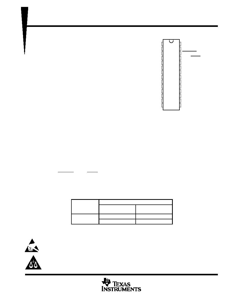
1
2
3
4
5
6
7
8
9
10
11
12
13
14
28
27
26
25
24
23
22
21
20
19
18
17
16
15
V
CC ≠
REF
ANLG COMMON
INT OUT
AUTO ZERO
BUFF OUT
C
ref ≠
C
ref +
IN ≠
IN +
V
CC +
D5
B1
B2
UNDER RANGE
OVER RANGE
STROBE
RUN/HOLD
DGTL GND
POLARITY
CLK
BUSY
D1
D2
D3
D4
B8
B4
DW OR N PACKAGE
(TOP VIEW)
ICL7135C, TLC7135C
4 1/2-DIGIT PRECISION
ANALOG-TO-DIGITAL CONVERTERS
SLAS074B ≠ DECEMBER 1986 ≠ REVISED MAY 1999
2
POST OFFICE BOX 655303
∑
DALLAS, TEXAS 75265
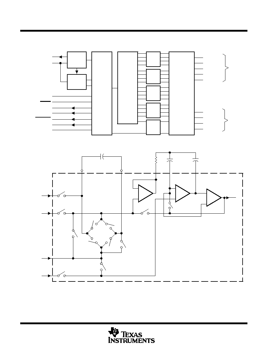
functional block diagram
17
12
18
8
A/Z, DE(
±
), Z/I
INT
BUFF
OUT
6
ANLG
COMMON
IN ≠
IN +
REF
9
3
10
2
A/Z
INT
Z/I
A/Z
DE(+)
DE(≠)
DE(+)
DE(≠)
A/Z
Input
Low
Input
High
A/Z
Buffer
+
≠
+
≠
+
≠
Comparator
Integrator
7
Cref +
Cref
RINT
CAZ
ANALOG SECTION
Binary
Coded
Decimal
Output
B4
15
B2
14
16
B8 (MSB)
13
B1 (LSB)
Digit
Drive
Output
D5 (MSD)
D4
D3
D2
D1 (LSD)
19
20
Multiplexer
Latch
Latch
Latch
Latch
Latch
Counters
Control
Logic
Zero
Cross
Detect
Polarity
Flip-Flop
DGTL GND
BUSY
STROBE
UNDER RANGE
OVER RANGE
RUN/HOLD
CLK
POLARITY
From Analog
Section
24
21
26
28
27
25
22
23
CINT
INT OUT
4
To
Digital
Section
5
Cref ≠
DIGITAL SECTION
AUTO
ZERO
ICL7135C, TLC7135C
4 1/2-DIGIT PRECISION
ANALOG-TO-DIGITAL CONVERTERS
SLAS074B ≠ DECEMBER 1986 ≠ REVISED MAY 1999
3
POST OFFICE BOX 655303
∑
DALLAS, TEXAS 75265
absolute maximum ratings over operating free-air temperature range (unless otherwise noted)
Supply voltage (V
CC+
with respect to V
CC ≠
) 15
V
. . . . . . . . . . . . . . . . . . . . . . . . . . . . . . . . . . . . . . . . . . . . . . . . . .
Analog input voltage (IN ≠ or IN +)
V
CC ≠
to V
CC+
. . . . . . . . . . . . . . . . . . . . . . . . . . . . . . . . . . . . . . . . . . . . . . . . . . .
Reference voltage range
V
CC ≠
to V
CC+
. . . . . . . . . . . . . . . . . . . . . . . . . . . . . . . . . . . . . . . . . . . . . . . . . . . . . . . . . . .
Clock input voltage range
0 V to V
CC+
. . . . . . . . . . . . . . . . . . . . . . . . . . . . . . . . . . . . . . . . . . . . . . . . . . . . . . . . . . . .
Operating free-air temperature range, T
A
0
∞
C to 70
∞
C
. . . . . . . . . . . . . . . . . . . . . . . . . . . . . . . . . . . . . . . . . . . . . .
Storage temperature range, T
stg
≠ 65
∞
C to 150
∞
C
. . . . . . . . . . . . . . . . . . . . . . . . . . . . . . . . . . . . . . . . . . . . . . . . . . .
Lead temperature 1,6 mm (1/16 inch) from case for 10 seconds: N package
260
∞
C
. . . . . . . . . . . . . . . . . . . . .
Stresses beyond those listed under "absolute maximum ratings" may cause permanent damage to the device. These are stress ratings only, and
functional operation of the device at these or any other conditions beyond those indicated under "recommended operating conditions" is not
implied. Exposure to absolute-maximum-rated conditions for extended periods may affect device reliability.
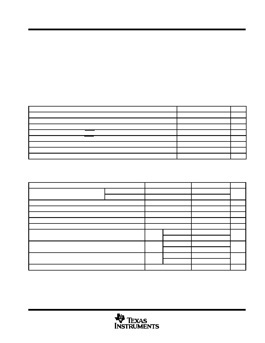
recommended operating conditions
MIN
NOM
MAX
UNIT
Supply voltage, VCC+
4
5
6
V
Supply voltage, VCC≠
≠ 3
≠ 5
≠ 8
V
Reference voltage, Vref
1
V
High-level input voltage, CLK, RUN/HOLD, VIH
2.8
V
Low-level input voltage, CLK, RUN/HOLD, VIL
0.8
V
Differential input voltage, VID
VCC ≠ +1
VCC+ ≠ 0.5
V
Maximum operating frequency, fclock (see Note 1)
1.2
2
MHz
Operating free-air temperature range, TA
0
70
∞
C
NOTE 1: Clock frequency range extends down to 0 Hz.
electrical characteristics, V
CC +
= 5 V, V
CC ≠
= 5 V, V
ref
= 1 V, f
clock
= 120 kHz, T
A
= 25
∞
C (unless
otherwise noted)
PARAMETER
TEST CONDITIONS
MIN
TYP
MAX
UNIT
VOH
High level output voltage
D1-D5, B1,B2,B4,B8
IO = ≠ 1 mA
2.4
5
V
VOH
High-level output voltage
Other outputs
IO = ≠ 10
µ
A
4.9
5
V
VOL
Low-level output voltage
IO = 1.6 mA
0.4
V
VON(PP) Peak-to-peak output noise voltage (see Note 2)
VID = 0,
Full scale = 2 V
15
µ
V
VO
Zero-reading temperature coefficient of output voltage
VID = 0,
0
∞
C
TA
70
∞
C
0.5
2
µ
V/
∞
C
IIH
High-level input current
VI = 5 V,
0
∞
C
TA
70
∞
C
0.1
10
µ
A
IIL
Low-level input current
VI = 0 V,
0
∞
C
TA
70
∞
C
≠ 0.02
≠ 0.1
mA
II
Input leakage current IN
and IN +
VID = 0
TA = 25
∞
C
1
10
pA
II
Input leakage current, IN ≠ and IN +
VID = 0
0
∞
C
TA
70
∞
C
250
pA
ICC
Positive supply current
f l k = 0
TA = 25
∞
C
1
2
mA
ICC +
Positive supply current
fclock = 0
0
∞
C
TA
70
∞
C
3
mA
ICC
Negative supply current
f l k = 0
TA = 25
∞
C
≠ 0.8
≠ 2
mA
ICC ≠
Negative supply current
fclock = 0
0
∞
C
TA
70
∞
C
≠ 3
mA
Cpd
Power dissipation capacitance
See Note 3
40
pF
NOTES:
2. This is the peak-to-peak value that is not exceeded 95% of the time.
3. Factor-relating clock frequency to increase in supply current. At VCC+ = 5 V, ICC+ = ICC+(fclock = 0) + Cpd
◊
5 V
◊
fclock
ICL7135C, TLC7135C
4 1/2-DIGIT PRECISION
ANALOG-TO-DIGITAL CONVERTERS
SLAS074B ≠ DECEMBER 1986 ≠ REVISED MAY 1999
4
POST OFFICE BOX 655303
∑
DALLAS, TEXAS 75265
operating characteristics, V
CC +
= 5 V, V
CC
≠ = 5 V, V
ref
= 1 V, f
clock
= 120 kHz, T
A
= 25
∞
C (unless
otherwise noted)
PARAMETER
TEST CONDITIONS
MIN
TYP
MAX
UNIT
FS
Full-scale temperature coefficient (see Note 4)
VID = 2 V,
0
∞
C
TA
70
∞
C
5
ppm/
∞
C
EL
Linearity error
≠ 2 V
VID
2 V
0.5
count
ED
Differential linearity error (see Note 5)
≠ 2 V
VID
2 V
0.01
LSB
EFS
±
Full-scale symmetry error (rollover error) (see Note 6)
VID =
±
2 V
0.5
1
count
Display reading with 0-V input
VID = 0,
0
∞
C
TA
70
∞
C
≠ 0.0000
±
0.0000
0.0000
Digital
Reading
Display reading in ratiometric operation
VID = Vref, TA = 25
∞
C
0.9998
0.9999
1.0000
Digital
Display reading in ratiometric operation
0
∞
C
TA
70
∞
C
0.9995
0.9999
1.0005
g
Reading
NOTES:
4. This parameter is measured with an external reference having a temperature coefficient of less than 0.01 ppm/
∞
C.
5. The magnitude of the difference between the worst case step of adjacent counts and the ideal step.
6. Rollover error is the difference between the absolute values of the conversion for 2 V and ≠ 2 V.
timing diagrams
D1
D2
D3
D4
D5
STROBE
B1 ≠ B8
201 Counts
200 Counts
D5
D1
D2
D3
D4
D5
BUSY
End of Conversion
200 Counts
200 Counts
200 Counts
200 Counts
200 Counts
Delay between BUSY going low and the first STROBE pulse is dependent upon the analog input.
Figure 1

ICL7135C, TLC7135C
4 1/2-DIGIT PRECISION
ANALOG-TO-DIGITAL CONVERTERS
SLAS074B ≠ DECEMBER 1986 ≠ REVISED MAY 1999
5
POST OFFICE BOX 655303
∑
DALLAS, TEXAS 75265
timing diagrams (continued)
D1
D2
D3
D4
D5
1000 Counts
Digital Scan
for OVER-RANGE
Figure 2
Integrator Output
OVER RANGE
When Applicable
BUSY
Full Measurement Cycle
40,002 Counts
De-Integrate
20,001 Counts Max
Signal Int
10,000
Counts
AUTO ZERO
10,001 Counts
UNDER RANGE
When Applicable
Figure 3