 | –≠–ª–µ–∫—Ç—Ä–æ–Ω–Ω—ã–π –∫–æ–º–ø–æ–Ω–µ–Ω—Ç: 74273 | –°–∫–∞—á–∞—Ç—å:  PDF PDF  ZIP ZIP |

1
Data sheet acquired from Harris Semiconductor
SCHS174
Features
∑ Common Clock and Asynchronous Master Reset
∑ Positive Edge Triggering
∑ Buffered Inputs
∑ Typical f
MAX
= 60MHz at V
CC
= 5V, C
L
= 15pF,
T
A
= 25
o
C
∑ Fanout (Over Temperature Range)
- Standard Outputs . . . . . . . . . . . . . . . 10 LSTTL Loads
- Bus Driver Outputs . . . . . . . . . . . . . 15 LSTTL Loads
∑ Wide Operating Temperature Range . . . -55
o
C to 125
o
C
∑ Balanced Propagation Delay and Transition Times
∑ Significant Power Reduction Compared to LSTTL
Logic ICs
∑ HC Types
- 2V to 6V Operation
- High Noise Immunity: N
IL
= 30%, N
IH
= 30% of V
CC
at V
CC
= 5V
∑ HCT Types
- 4.5V to 5.5V Operation
- Direct LSTTL Input Logic Compatibility,
V
IL
= 0.8V (Max), V
IH
= 2V (Min)
- CMOS Input Compatibility, I
l
1
µ
A at V
OL
, V
OH
Description
The Harris CD74HC273 and CD74HCT273 high speed octal
D-Type flip-flops with a direct clear input are manufactured
with silicon-gate CMOS technology. They possess the low
power consumption of standard CMOS integrated circuits.
Information at the D inputis transferred to the Q outputs on
the positive-going edge of the clock pulse. All eight flip-flops
are controlled by a common clock (CP) and a common reset
(MR). Resetting is accomplished by a low voltage level
independent of the clock. All eight Q outputs are reset to a
logic 0.
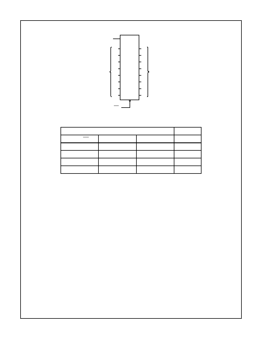
Pinout
CD54HC273, CD54HCT273, CD74HC273, CD74HCT273
(PDIP, SOIC, CERDIP)
TOP VIEW
Ordering Information
PART NUMBER
TEMP. RANGE
(
o
C)
PACKAGE
PKG.
NO.
CD54HC273F
-55 to 125
20 Ld CERDIP
F20.3
CD54HCT273F
-55 to 125
20 Ld CERDIP
F20.3
CD74HC273E
-55 to 125
20 Ld PDIP
E20.3
CD74HCT273E
-55 to 125
20 Ld PDIP
E20.3
CD74HC273M
-55 to 125
20 Ld SOIC
M20.3
CD74HCT273M
-55 to 125
20 Ld SOIC
M20.3
NOTES:
1. When ordering, use the entire part number. Add the suffix 96 to
obtain the variant in the tape and reel.
2. Wafer and die for this part number is available which meets all
electrical specifications. Please contact your local sales office or
Harris customer service for ordering information.
11
12
13
14
15
16
17
18
20
19
10
9
8
7
6
5
4
3
2
1
MR
Q0
D0
D1
Q1
Q2
D3
D2
Q3
GND
V
CC
D7
D6
Q6
Q7
Q5
D5
D4
Q4
CP
February 1998
CAUTION: These devices are sensitive to electrostatic discharge. Users should follow proper IC Handling Procedures.
Copyright
©
Harris Corporation 1998
CD74HC273,
CD74HCT273
High Speed CMOS Logic
Octal D-Type Flip-Flop with Reset
File Number
1479.2
[ /Title
(CD74
HC273
,
CD74
HCT27
3)
/Sub-
ject
(High
Speed
CMOS
Logic
Octal
D-
Type
Flip-
2
Functional Diagram
TRUTH TABLE
INPUTS
OUTPUT
RESET (MR)
CLOCK CP
DATA D
n
Q
L
X
X
L
H
H
H
H
L
L
H
L
X
Q
0
NOTE: H = High Voltage Level, L = Low Voltage Level, X = Don't Care,
= Transition from Low
to High Level, Q
0
= Level Before the Indicated Steady-State Input Conditions Were Established.
Q0
Q1
Q2
Q3
Q4
Q5
Q6
Q7
RESET MR
D0
D1
D2
D3
D4
D5
D6
D7
CLOCK
CP
DATA
INPUTS
DATA
OUTPUTS
CD74HC273, CD74HCT273

3
Absolute Maximum Ratings
Thermal Information
DC Supply Voltage, V
CC
. . . . . . . . . . . . . . . . . . . . . . . . -0.5V to 7V
DC Input Diode Current, I
IK
For V
I
< -0.5V or V
I
> V
CC
+ 0.5V
. . . . . . . . . . . . . . . . . . . . . .±
20mA
DC Output Diode Current, I
OK
For V
O
< -0.5V or V
O
> V
CC
+ 0.5V
. . . . . . . . . . . . . . . . . . . .±
20mA
DC Drain Current, per Output, I
O
For -0.5V < V
O
< V
CC
+ 0.5V
. . . . . . . . . . . . . . . . . . . . . . . . . .±
25mA
DC Output Source or Sink Current per Output Pin, I
O
For V
O
> -0.5V or V
O
< V
CC
+ 0.5V
. . . . . . . . . . . . . . . . . . . .±
25mA
DC V
CC
or Ground Current, I
CC
. . . . . . . . . . . . . . . . . . . . . . . . .±
50mA
Operating Conditions
Temperature Range, T
A
. . . . . . . . . . . . . . . . . . . . . . -55
o
C to 125
o
C
Supply Voltage Range, V
CC
HC Types . . . . . . . . . . . . . . . . . . . . . . . . . . . . . . . . . . . . .2V to 6V
HCT Types . . . . . . . . . . . . . . . . . . . . . . . . . . . . . . . . .4.5V to 5.5V
DC Input or Output Voltage, V
I
, V
O
. . . . . . . . . . . . . . . . . 0V to V
CC
Input Rise and Fall Time
2V . . . . . . . . . . . . . . . . . . . . . . . . . . . . . . . . . . . . . . 1000ns (Max)
4.5V. . . . . . . . . . . . . . . . . . . . . . . . . . . . . . . . . . . . . . 500ns (Max)
6V . . . . . . . . . . . . . . . . . . . . . . . . . . . . . . . . . . . . . . . 400ns (Max)
Thermal Resistance (Typical, Note 3)
JA
(
o
C/W)
JC
(
o
C/W)
PDIP Package . . . . . . . . . . . . . . . . . . .
125
N/A
CERDIP Package . . . . . . . . . . . . . . . .
105
44
SOIC Package . . . . . . . . . . . . . . . . . . .
120
N/A
Maximum Junction Temperature . . . . . . . . . . . . . . . . . . . . . . . 150
o
C
Maximum Storage Temperature Range . . . . . . . . . .-65
o
C to 150
o
C
Maximum Lead Temperature (Soldering 10s) . . . . . . . . . . . . . 300
o
C
(SOIC - Lead Tips Only)
CAUTION: Stresses above those listed in "Absolute Maximum Ratings" may cause permanent damage to the device. This is a stress only rating and operation
of the device at these or any other conditions above those indicated in the operational sections of this specification is not implied.
NOTE:
3.
JA
is measured with the component mounted on an evaluation PC board in free air.
DC Electrical Specifications
PARAMETER
SYMBOL
TEST
CONDITIONS
V
CC
(V)
25
o
C
-40
o
C TO 85
o
C
-55
o
C TO 125
o
C
UNITS
V
I
(V)
I
O
(mA)
MIN
TYP
MAX
MIN
MAX
MIN
MAX
HC TYPES
High Level Input
Voltage
V
IH
-
-
2
1.5
-
-
1.5
-
1.5
-
V
4.5
3.15
-
-
3.15
-
3.15
-
V
6
4.2
-
-
4.2
-
4.2
-
V
Low Level Input
Voltage
V
IL
-
-
2
-
-
0.5
-
0.5
-
0.5
V
4.5
-
-
1.35
-
1.35
-
1.35
V
6
-
-
1.8
-
1.8
-
1.8
V
High Level Output
Voltage
CMOS Loads
V
OH
V
IH
or
V
IL
-0.02
2
1.9
-
-
1.9
-
1.9
-
V
-0.02
4.5
4.4
-
-
4.4
-
4.4
-
V
-0.02
6
5.9
-
-
5.9
-
5.9
-
V
High Level Output
Voltage
TTL Loads
-4
4.5
3.98
-
-
3.84
-
3.7
-
V
-5.2
6
5.48
-
-
5.34
-
5.2
-
V
Low Level Output
Voltage
CMOS Loads
V
OL
V
IH
or
V
IL
0.02
2
-
-
0.1
-
0.1
-
0.1
V
0.02
4.5
-
-
0.1
-
0.1
-
0.1
V
0.02
6
-
-
0.1
-
0.1
-
0.1
V
Low Level Output
Voltage
TTL Loads
4
4.5
-
-
0.26
-
0.33
-
0.4
V
5.2
6
-
-
0.26
-
0.33
-
0.4
V
Input Leakage
Current
I
I
V
CC
or
GND
-
6
-
-
±
0.1
-
±
1
-
±
1
µ
A
Quiescent Device
Current
I
CC
V
CC
or
GND
0
6
-
-
8
-
80
-
160
µ
A
CD74HC273, CD74HCT273

4
HCT TYPES
High Level Input
Voltage
V
IH
-
-
4.5 to
5.5
2
-
-
2
-
2
-
V
Low Level Input
Voltage
V
IL
-
-
4.5 to
5.5
-
-
0.8
-
0.8
-
0.8
V
High Level Output
Voltage
CMOS Loads
V
OH
V
IH
or
V
IL
-0.02
4.5
4.4
-
-
4.4
-
4.4
-
V
High Level Output
Voltage
TTL Loads
-4
4.5
3.98
-
-
3.84
-
3.7
-
V
Low Level Output
Voltage
CMOS Loads
V
OL
V
IH
or
V
IL
0.02
4.5
-
-
0.1
-
0.1
-
0.1
V
Low Level Output
Voltage
TTL Loads
4
4.5
-
-
0.26
-
0.33
-
0.4
V
Input Leakage
Current
I
I
V
CC
to
GND
0
5.5
-
-
±
0.1
-
±
1
-
±
1
µ
A
Quiescent Device
Current
I
CC
V
CC
or
GND
0
5.5
-
-
8
-
80
-
160
µ
A
Additional Quiescent
Device Current Per
Input Pin: 1 Unit Load
(Note 4)
I
CC
V
CC
-2.1
-
4.5 to
5.5
-
100
360
-
450
-
490
µ
A
NOTE:
4. For dual-supply systems theoretical worst case (V
I
= 2.4V, V
CC
= 5.5V) specification is 1.8mA.
DC Electrical Specifications
(Continued)
PARAMETER
SYMBOL
TEST
CONDITIONS
V
CC
(V)
25
o
C
-40
o
C TO 85
o
C
-55
o
C TO 125
o
C
UNITS
V
I
(V)
I
O
(mA)
MIN
TYP
MAX
MIN
MAX
MIN
MAX
HCT Input Loading Table
INPUT
UNIT LOADS
MR
1.5
Data
0.4
CP
1.5
NOTE: Unit Load is
I
CC
limit specified in DC Electrical
Specifications table, e.g., 360
µ
A max at 25
o
C.
Prerequisite For Switching Specifications
PARAMETER
SYMBOL
TEST
CONDITIONS
V
CC
(V)
25
o
C
-40
o
C TO 85
o
C
-55
o
C TO 125
o
C
UNITS
MIN
TYP
MAX
MIN
MAX
MIN
MAX
HC TYPES
Maximum Clock Frequency
(Figure 1)
f
MAX
-
2
6
-
-
5
-
4
-
MHz
4.5
30
-
-
25
-
20
-
MHz
6
35
-
-
29
-
23
-
MHz
MR Pulse Width
(Figure 1)
t
W
-
2
60
-
-
75
-
90
-
ns
4.5
12
-
-
15
-
18
-
ns
6
10
-
-
13
-
15
-
ns
CD74HC273, CD74HCT273

5
Clock Pulse Width (Figure 1)
t
W
-
2
80
-
-
100
-
120
-
ns
4.5
16
-
-
20
-
24
-
ns
6
14
-
-
17
-
20
-
ns
Set-up Time Data to Clock
(Figure 5)
t
SU
-
2
60
-
-
75
-
70
-
ns
4.5
12
-
-
15
-
18
-
ns
6
10
-
-
13
-
15
-
ns
Hold Time, Data to Clock
(Figure 5)
t
H
-
2
3
-
-
3
-
3
-
ns
4.5
3
-
-
3
-
3
-
ns
6
3
-
-
3
-
3
-
ns
Removal Time, MR to Clock
t
REM
-
2
50
-
-
65
-
75
-
ns
4.5
10
-
-
13
-
15
-
ns
6
9
-
-
11
-
13
-
ns
HCT TYPES
Maximum Clock Frequency
(Figure 2)
f
MAX
-
4.5
25
-
-
20
-
16
-
MHz
MR Pulse Width
(Figure 2)
t
w
-
4.5
12
-
-
15
-
18
-
ns
Clock Pulse Width (Figure 2)
t
w
-
4.5
20
-
-
25
-
30
-
ns
Set-up Time Data to Clock
(Figure 6)
t
SU
-
4.5
12
-
-
15
-
18
-
ns
Hold Time, Data to Clock
(Figure 6)
t
H
-
4.5
3
-
-
3
-
3
-
ns
Removal Time, MR to Clock
t
REM
-
4.5
10
-
-
13
-
15
-
ns
Switching Specifications
Input t
r
, t
f
= 6ns
PARAMETER
SYMBOL
TEST
CONDITIONS
V
CC
(V)
25
o
C
-40
o
C TO 85
o
C
-55
o
C TO
125
o
C
UNITS
TYP
MAX
MAX
MAX
HC TYPES
Propagation Delay,
Clock to Output
(Figure 3)
t
PLH
, t
PHL
C
L
= 50pF
2
-
150
190
225
ns
4.5
-
30
38
45
ns
6
-
26
30
38
ns
C
L
= 15pF
5
12
-
-
-
ns
Propagation Delay,
MR to Output
(Figure 3)
t
PHL
C
L
= 50pF
2
-
150
190
225
ns
4.5
-
30
38
45
ns
6
-
26
30
38
ns
Output Transition Time
(Figure 3)
t
TLH
, t
THL
C
L
= 50pF
2
-
75
95
110
ns
4.5
-
15
19
22
ns
6
-
13
16
19
ns
Input Capacitance
C
I
-
-
-
10
10
10
pF
Maximum Clock Frequency
f
MAX
C
L
= 15pF
5
60
-
-
-
MHz
Prerequisite For Switching Specifications
(Continued)
PARAMETER
SYMBOL
TEST
CONDITIONS
V
CC
(V)
25
o
C
-40
o
C TO 85
o
C
-55
o
C TO 125
o
C
UNITS
MIN
TYP
MAX
MIN
MAX
MIN
MAX
CD74HC273, CD74HCT273