www.ti.com
FEATURES
DESCRIPTION
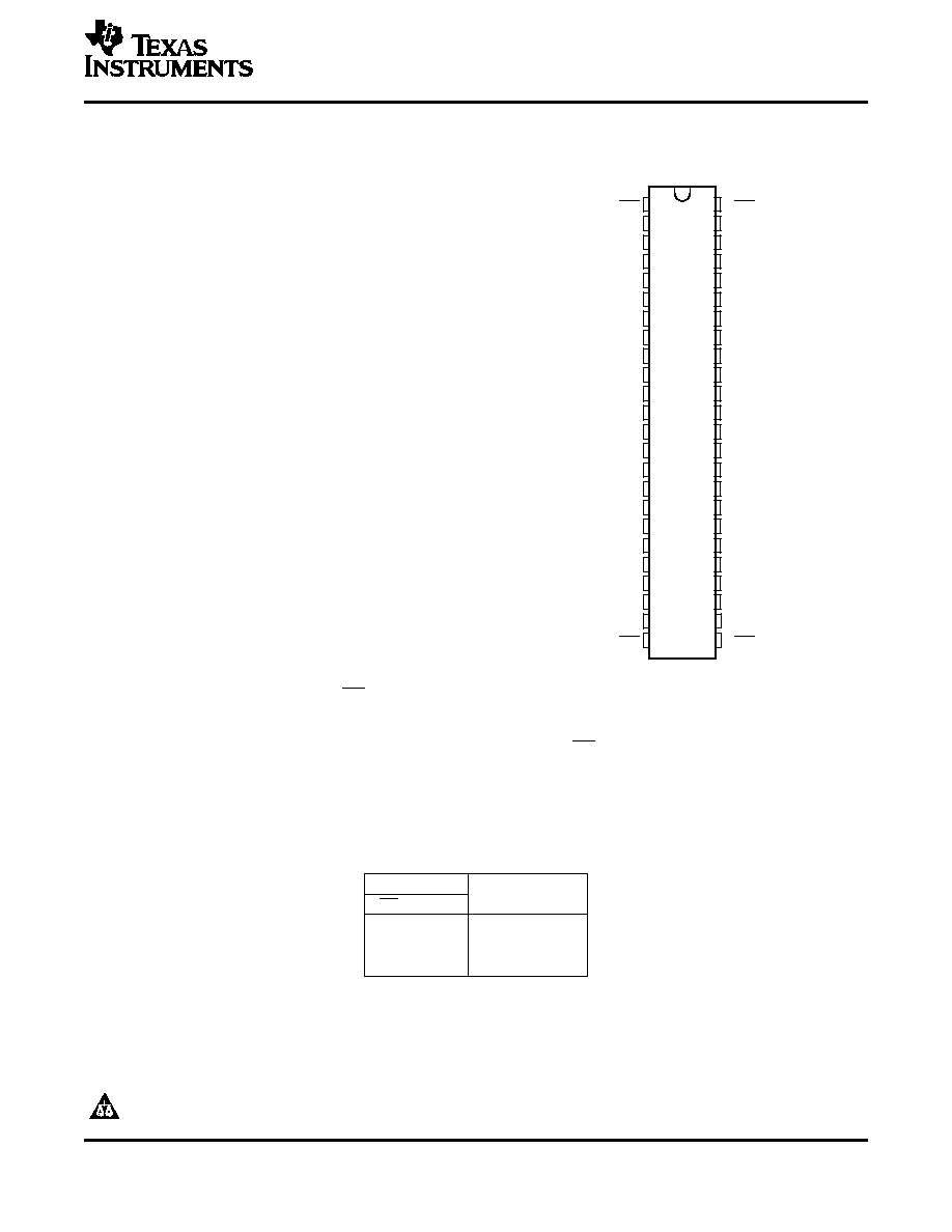
SN54ABT16244 . . . WD PACKAGE
SN74ABT16244A . . . DGG, DGV, OR DL PACKAGE
(TOP VIEW)
1
2
3
4
5
6
7
8
9
10
11
12
13
14
15
16
17
18
19
20
21
22
23
24
48
47
46
45
44
43
42
41
40
39
38
37
36
35
34
33
32
31
30
29
28
27
26
25
1OE
1Y1
1Y2
GND
1Y3
1Y4
V
CC
2Y1
2Y2
GND
2Y3
2Y4
3Y1
3Y2
GND
3Y3
3Y4
V
CC
4Y1
4Y2
GND
4Y3
4Y4
4OE
2OE
1A1
1A2
GND
1A3
1A4
V
CC
2A1
2A2
GND
2A3
2A4
3A1
3A2
GND
3A3
3A4
V
CC
4A1
4A2
GND
4A3
4A4
3OE
To ensure the high-impedance state during power up or power down, OE should be tied to V
CC
through a pullup
SN54ABT16244, SN74ABT16244A
16-BIT BUFFERS/DRIVERS
WITH 3-STATE OUTPUTS
SCBS073H ≠ SEPTEMBER 1991 ≠ REVISED AUGUST 2005
∑
Members of the Texas Instruments
WidebusTM Family
∑
State-of-the-Art EPIC-IIBTM BiCMOS Design
Significantly Reduces Power Dissipation
∑
Latch-Up Performance Exceeds 500 mA Per
JESD 70
∑
Typical V
OLP
(Output Ground Bounce) <1 V
at V
CC
= 5 V, T
A
= 25
∞
C
∑
Distributed V
CC
and GND Pin Configuration
Minimizes High-Speed Switching Noise
∑
Flow-Through Architecture Optimizes PCB
Layout
∑
High-Drive Outputs (≠32-mA I
OH
, 64-mA I
OL
)
∑
Package Options Include Plastic 300-mil
Shrink Small-Outline (DL), Thin Shrink
Small-Outline (DGG), and Thin Very
Small-Outline (DGV) Packages and 380-mil
Fine-Pitch Ceramic Flat (WD) Package
Using 25-mil Center-to-Center Spacings
The SN54ABT16244 and SN74ABT16244A are 16-bit
buffers and line drivers designed specifically to
improve both the performance and density of 3-state
memory
address
drivers,
clock
drivers,
and
bus-oriented
receivers
and
transmitters.
These
devices can be used as four 4-bit buffers, two 8-bit
buffers, or one 16-bit buffer. These devices provide
true
outputs
and
symmetrical
OE
(active-low
output-enable) inputs.
resistor; the minimum value of the resistor is determined by the current-sinking capability of the driver.
The SN54ABT16244 is characterized for operation over the full military temperature range of ≠55
∞
C to 125
∞
C.
The SN74ABT16244A is characterized for operation from ≠40
∞
C to 85
∞
C.
FUNCTION TABLE
(EACH BUFFER)
INPUTS
OUTPUT
Y
OE
A
L
H
H
L
L
L
H
X
Z
Please be aware that an important notice concerning availability, standard warranty, and use in critical applications of Texas
Instruments semiconductor products and disclaimers thereto appears at the end of this data sheet.
Widebus, EPIC-IIB are trademarks of Texas Instruments.
PRODUCTION DATA information is current as of publication date.
Copyright © 1991≠2005, Texas Instruments Incorporated
Products conform to specifications per the terms of the Texas
On products compliant to MIL-PRF-38535, all parameters are
Instruments standard warranty. Production processing does not
tested unless otherwise noted. On all other products, production
necessarily include testing of all parameters.
processing does not necessarily include testing of all parameters.

www.ti.com
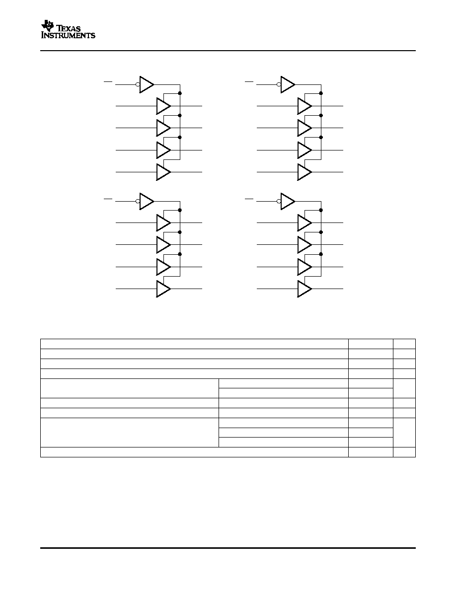
47
1A1
46
1A2
44
1A3
43
1A4
1Y1
2
1Y2
3
1Y3
5
1Y4
6
41
2A1
40
2A2
38
2A3
37
2A4
2Y1
8
2Y2
9
2Y3
11
2Y4
12
36
3A1
35
3A2
33
3A3
32
3A4
3Y1
13
3Y2
14
3Y3
16
3Y4
17
30
4A1
29
4A2
27
4A3
26
4A4
4Y1
19
4Y2
20
4Y3
22
4Y4
23
EN1
1
EN4
24
1OE
2OE
3OE
4OE
EN2
48
EN3
25
(1) This symbol is in accordance with ANSI/IEEE Std 91-1984 and
IEC Publication 617-12.
1
1
1
1
1
2
3
4
SN54ABT16244, SN74ABT16244A
16-BIT BUFFERS/DRIVERS
WITH 3-STATE OUTPUTS
SCBS073H ≠ SEPTEMBER 1991 ≠ REVISED AUGUST 2005
LOGIC SYMBOL
(1)
2
www.ti.com
1OE
1A1
1A2
1A3
1A4
1Y1
1Y2
1Y3
1Y4
1
47
46
44
43
2
3
5
6
2OE
2A1
2A2
2A3
2A4
2Y1
2Y2
2Y3
2Y4
48
41
40
38
37
8
9
11
12
3OE
3A1
3A2
3A3
3A4
3Y1
3Y2
3Y3
3Y4
25
36
35
33
32
13
14
16
17
4OE
4A1
4A2
4A3
4A4
4Y1
4Y2
4Y3
4Y4
24
30
29
27
26
19
20
22
23
Absolute Maximum Ratings
(1)
SN54ABT16244, SN74ABT16244A
16-BIT BUFFERS/DRIVERS
WITH 3-STATE OUTPUTS
SCBS073H ≠ SEPTEMBER 1991 ≠ REVISED AUGUST 2005
LOGIC DIAGRAM (POSITIVE LOGIC)
over operating free-air temperature range (unless otherwise noted)
MIN
MAX
UNIT
V
CC
Supply voltage range
≠0.5
7
V
V
I
Input voltage range
(2)
≠0.5
7
V
V
O
Voltage range applied to any output in the high or power-off state
≠0.5
5.5
V
SN54ABT16244
96
I
O
Current into any output in the low state
mA
SN74ABT16244A
128
I
IK
Input clamp current
V
I
< 0
≠18
mA
I
OK
Output clamp current
V
O
< 0
≠50
mA
DGG package
89
JA
Package thermal impedance
(3)
DGV package
93
∞
C/W
DL package
94
T
stg
Storage temperature range
≠65
150
∞
C
(1)
Stresses beyond those listed under "absolute maximum ratings" may cause permanent damage to the device. These are stress ratings
only, and functional operation of the device at these or any other conditions beyond those indicated under "recommended operating
conditions" is not implied. Exposure to absolute-maximum-rated conditions for extended periods may affect device reliability
(2)
The input and output negative-voltage ratings may be exceeded if the input and output clamp-current ratings are observed.
(3)
The package thermal impedance is calculated in accordance with EIA/JEDEC Std JESD 51.
3

www.ti.com
Recommended Operating Conditions
(1)
Electrical Characteristics
SN54ABT16244, SN74ABT16244A
16-BIT BUFFERS/DRIVERS
WITH 3-STATE OUTPUTS
SCBS073H ≠ SEPTEMBER 1991 ≠ REVISED AUGUST 2005
SN54ABT16244
SN74ABT16244A
UNIT
MIN
MAX
MIN
MAX
V
CC
Supply voltage
4.5
5.5
4.5
5.5
V
V
IH
High-level input voltage
2
2
V
V
IL
Low-level input voltage
0.8
0.8
V
V
I
Input voltage
0
V
CC
0
V
CC
V
I
OH
High-level output current
≠24
≠32
mA
I
OL
Low-level output current
48
64
mA
t/
v
Input transition rise or fall rate
Outputs enabled
10
10
ns/V
T
A
Operating free-air temperature
≠55
125
≠40
85
∞
C
(1)
All unused inputs of the device must be held at V
CC
or GND to ensure proper device operation. Refer to the TI application report,
Implications of Slow or Floating CMOS Inputs, literature number SCBA004.
over recommended operating free-air temperature range (unless otherwise noted)
T
A
= 25
∞
C
(1)
SN54ABT16244
SN74ABT16244A
PARAMETER
TEST CONDITIONS
UNIT
MIN TYP
(2)
MAX
MIN
MAX
MIN
MAX
V
IK
V
CC
= 4.5 V,
I
I
= ≠18 mA
≠1.2
≠1.2
≠1.2
V
V
CC
= 4.5 V,
I
OH
= ≠3 mA
2.5
2.5
2.5
V
CC
= 5 V,
I
OH
= ≠3 mA
3
3
3
V
OH
V
I
OH
= ≠24 mA
2
2
V
CC
= 4.5 V
I
OH
= ≠32 mA
2
(3)
2
I
OL
= 48 mA
0.55
0.55
V
OL
V
CC
= 4.5 V
V
I
OL
= 64 mA
0.55
(3)
0.55
V
hys
100
mV
I
I
V
CC
= 5.5 V, V
I
= V
CC
or GND
±
1
±
1
±
1
µ
A
I
OZH
V
CC
= 5.5 V,
V
O
= 2.7 V
10
(4)
10
10
(4)
µ
A
I
OZL
V
CC
= 5.5 V,
V
O
= 0.5 V
≠10
(4)
≠10
≠10
(4)
µ
A
I
off
V
CC
= 0,
V
I
or V
O
5.5 V
±
100
±
100
µ
A
V
CC
= 5.5 V,
I
CEX
Outputs high
50
50
50
µ
A
V
O
= 5.5 V
I
O
(5)
V
CC
= 5.5 V,
V
O
= 2.5 V
≠50
≠100
≠180
≠50
≠180
≠50
≠180
mA
Outputs high
3
2
3
V
CC
= 5.5 V,
I
CC
I
O
= 0,
Outputs low
32
32
32
mA
V
I
= V
CC
or GND
Outputs disabled
3
2
3
V
CC
= 5.5 V,
Outputs enabled
0.05
1.5
0.05
Data
One input at 3.4 V,
inputs
Other inputs at
Outputs disabled
0.05
1
0.05
I
CC
(6)
mA
V
CC
or GND
Control
V
CC
= 5.5 V, One input at 3.4 V,
0.05
1.5
0.05
inputs
Other inputs at V
CC
or GND
C
i
V
I
= 2.5 V or 0.5 V
3
pF
C
o
V
O
= 2.5 V or 0.5 V
6
pF
(1)
Characteristics for T
A
= 25
∞
C apply to the SN74ABT16244A only.
(2)
All typical values are at V
CC
= 5 V.
(3)
On products compliant to MIL-PRF-38535, this parameter does not apply.
(4)
This data-sheet limit may vary among suppliers.
(5)
Not more than one output should be tested at a time, and the duration of the test should not exceed one second.
(6)
This is the increase in supply current for each input that is at the specified TTL voltage level rather than V
CC
or GND.
4
www.ti.com
Switching Characteristics
Switching Characteristics
SN54ABT16244, SN74ABT16244A
16-BIT BUFFERS/DRIVERS
WITH 3-STATE OUTPUTS
SCBS073H ≠ SEPTEMBER 1991 ≠ REVISED AUGUST 2005
over recommended ranges of supply voltage and operating free-air temperature, C
L
= 50 pF
(unless otherwise noted) (see
Figure 1
)
SN54ABT16244
FROM
TO
V
CC
= 5 V,
PARAMETER
UNIT
(INPUT)
(OUTPUT)
T
A
= 25
∞
C
MIN
MAX
MIN
TYP
MAX
t
PLH
0.7
2.3
3.2
0.7
3.6
A
Y
ns
t
PHL
0.5
2.6
3.7
0.5
4.2
t
PZH
0.7
3
4
0.7
4.9
OE
Y
ns
t
PZL
0.9
3.2
5.5
0.9
6.5
t
PHZ
1.7
3.6
5
1.7
6
OE
Y
ns
t
PLZ
1.5
2.9
4.7
1.5
5.7
over recommended ranges of supply voltage and operating free-air temperature, C
L
= 50 pF
(unless otherwise noted) (see
Figure 1
)
SN74ABT16244A
FROM
TO
V
CC
= 5 V,
PARAMETER
UNIT
(INPUT)
(OUTPUT)
T
A
= 25
∞
C
MIN
MAX
MIN
TYP
MAX
t
PLH
1
2.3
3.2
1
3.5
A or B
Y
ns
t
PHL
1
2.6
3.7
1
4.1
t
PZH
1
3
3.8
1
4.8
OE
Y
ns
t
PZL
1
3.2
4
1
4.8
t
PHZ
1
3.6
4.4
1
4.8
OE
Y
ns
t
PLZ
1
2.9
3.7
1
4.1
5
www.ti.com
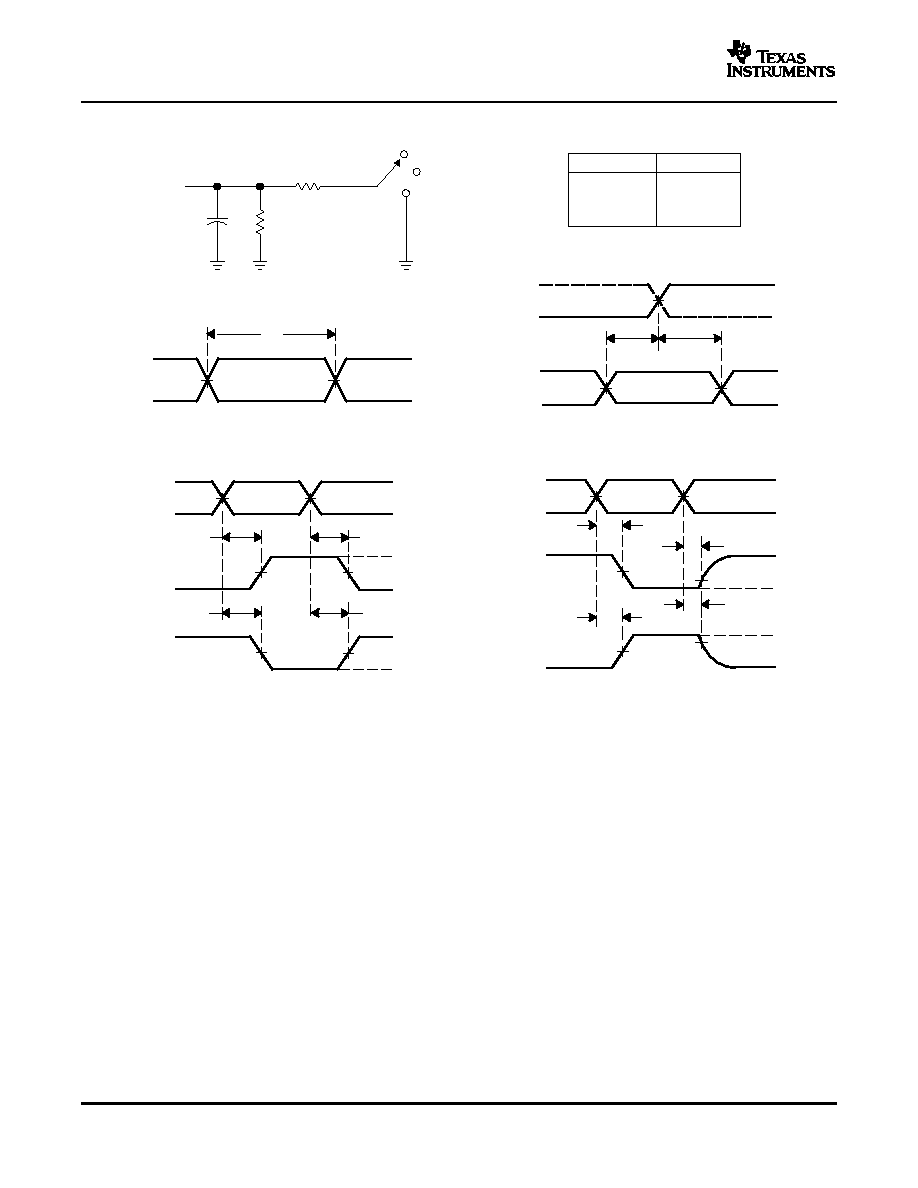
PARAMETER MEASUREMENT INFORMATION
1.5 V
t
h
t
su
From Output
Under Test
C
L
= 50 pF
(see Note A)
LOAD CIRCUIT
S1
7 V
Open
GND
500
500
Data Input
Timing Input
1.5 V
3 V
0 V
1.5 V
1.5 V
3 V
0 V
3 V
0 V
1.5 V
t
w
Input
VOLTAGE WAVEFORMS
SETUP AND HOLD TIMES
VOLTAGE WAVEFORMS
PROPAGATION DELAY TIMES
INVERTING AND NONINVERTING OUTPUTS
VOLTAGE WAVEFORMS
PULSE DURATION
t
PLH
t
PHL
t
PHL
t
PLH
V
OH
V
OH
V
OL
V
OL
1.5 V
1.5 V
3 V
0 V
1.5 V
1.5 V
Input
1.5 V
Output
Control
Output
Waveform 1
S1 at 7 V
(see Note B)
Output
Waveform 2
S1 at Open
(see Note B)
V
OL
V
OH
t
PZL
t
PZH
t
PLZ
t
PHZ
1.5 V
1.5 V
3.5 V
0 V
1.5 V
V
OL
+ 0.3 V
1.5 V
V
OH
- 0.3 V
0 V
3 V
VOLTAGE WAVEFORMS
ENABLE AND DISABLE TIMES
LOW- AND HIGH-LEVEL ENABLING
Output
Output
t
PLH
/t
PHL
t
PLZ
/t
PZL
t
PHZ
/t
PZH
Open
7 V
Open
TEST
S1
NOTES: A. C
L
includes probe and jig capacitance.
B. Waveform 1 is for an output with internal conditions such that the output is low, except when disabled by the output control.
Waveform 2 is for an output with internal conditions such that the output is high, except when disabled by the output control.
C. All input pulses are supplied by generators having the following characteristics: PRR
10 MHz, Z
O
= 50
, t
r
2.5 ns, t
f
2.5 ns.
D. The outputs are measured one at a time, with one transition per measurement.
1.5 V
SN54ABT16244, SN74ABT16244A
16-BIT BUFFERS/DRIVERS
WITH 3-STATE OUTPUTS
SCBS073H ≠ SEPTEMBER 1991 ≠ REVISED AUGUST 2005
Figure 1. Load Circuit and Voltage Waveforms
6

PACKAGING INFORMATION
Orderable Device
Status
(1)
Package
Type
Package
Drawing
Pins Package
Qty
Eco Plan
(2)
Lead/Ball Finish
MSL Peak Temp
(3)
5962-9317401MXA
ACTIVE
CFP
WD
48
1
TBD
Call TI
Level-NC-NC-NC
74ABT16244ADGGRG4
ACTIVE
TSSOP
DGG
48
2000 Green (RoHS &
no Sb/Br)
CU NIPDAU
Level-1-260C-UNLIM
74ABT16244ADGVRE4
ACTIVE
TVSOP
DGV
48
2000 Green (RoHS &
no Sb/Br)
CU NIPDAU
Level-1-260C-UNLIM
SN74ABT16244ADGGR
ACTIVE
TSSOP
DGG
48
2000 Green (RoHS &
no Sb/Br)
CU NIPDAU
Level-1-260C-UNLIM
SN74ABT16244ADGVR
ACTIVE
TVSOP
DGV
48
2000 Green (RoHS &
no Sb/Br)
CU NIPDAU
Level-1-260C-UNLIM
SN74ABT16244ADL
ACTIVE
SSOP
DL
48
25
Green (RoHS &
no Sb/Br)
CU NIPDAU
Level-1-260C-UNLIM
SN74ABT16244ADLG4
ACTIVE
SSOP
DL
48
25
Green (RoHS &
no Sb/Br)
CU NIPDAU
Level-1-260C-UNLIM
SN74ABT16244ADLR
ACTIVE
SSOP
DL
48
1000 Green (RoHS &
no Sb/Br)
CU NIPDAU
Level-1-260C-UNLIM
SN74ABT16244ADLRG4
ACTIVE
SSOP
DL
48
1000 Green (RoHS &
no Sb/Br)
CU NIPDAU
Level-1-260C-UNLIM
SNJ54ABT16244WD
ACTIVE
CFP
WD
48
1
TBD
Call TI
Level-NC-NC-NC
(1)
The marketing status values are defined as follows:
ACTIVE: Product device recommended for new designs.
LIFEBUY: TI has announced that the device will be discontinued, and a lifetime-buy period is in effect.
NRND: Not recommended for new designs. Device is in production to support existing customers, but TI does not recommend using this part in
a new design.
PREVIEW: Device has been announced but is not in production. Samples may or may not be available.
OBSOLETE: TI has discontinued the production of the device.
(2)
Eco
Plan
-
The
planned
eco-friendly
classification:
Pb-Free
(RoHS)
or
Green
(RoHS
&
no
Sb/Br)
-
please
check
http://www.ti.com/productcontent
for the latest availability information and additional product content details.
TBD: The Pb-Free/Green conversion plan has not been defined.
Pb-Free (RoHS): TI's terms "Lead-Free" or "Pb-Free" mean semiconductor products that are compatible with the current RoHS requirements
for all 6 substances, including the requirement that lead not exceed 0.1% by weight in homogeneous materials. Where designed to be soldered
at high temperatures, TI Pb-Free products are suitable for use in specified lead-free processes.
Green (RoHS & no Sb/Br): TI defines "Green" to mean Pb-Free (RoHS compatible), and free of Bromine (Br) and Antimony (Sb) based flame
retardants (Br or Sb do not exceed 0.1% by weight in homogeneous material)
(3)
MSL, Peak Temp. -- The Moisture Sensitivity Level rating according to the JEDEC industry standard classifications, and peak solder
temperature.
Important Information and Disclaimer:The information provided on this page represents TI's knowledge and belief as of the date that it is
provided. TI bases its knowledge and belief on information provided by third parties, and makes no representation or warranty as to the
accuracy of such information. Efforts are underway to better integrate information from third parties. TI has taken and continues to take
reasonable steps to provide representative and accurate information but may not have conducted destructive testing or chemical analysis on
incoming materials and chemicals. TI and TI suppliers consider certain information to be proprietary, and thus CAS numbers and other limited
information may not be available for release.
In no event shall TI's liability arising out of such information exceed the total purchase price of the TI part(s) at issue in this document sold by TI
to Customer on an annual basis.
PACKAGE OPTION ADDENDUM
www.ti.com
26-Sep-2005
Addendum-Page 1
MECHANICAL DATA
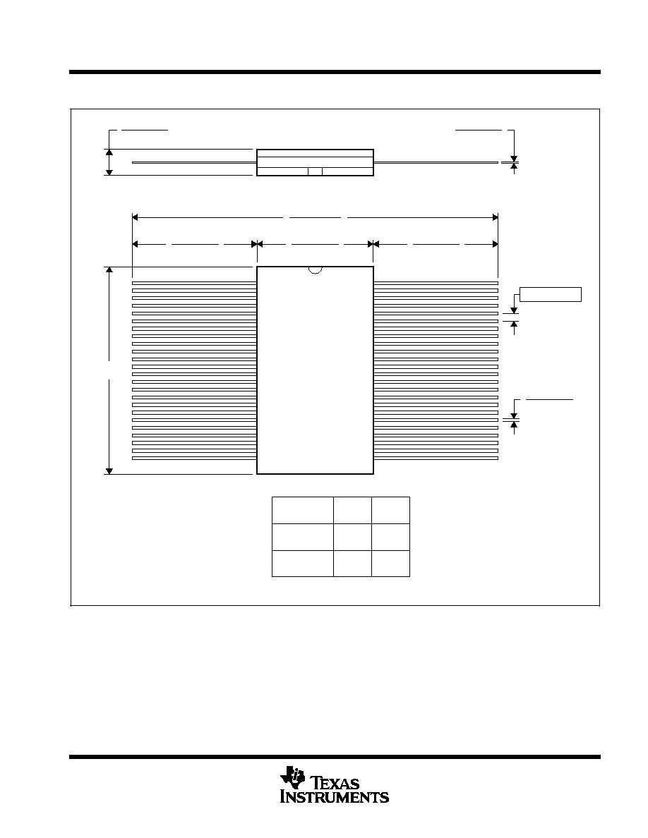
MCFP010B ≠ JANUARY 1995 ≠ REVISED NOVEMBER 1997
POST OFFICE BOX 655303
∑
DALLAS, TEXAS 75265
WD (R-GDFP-F**)
CERAMIC DUAL FLATPACK
4040176 / D 10/97
48 LEADS SHOWN
48
48
25
56
0.610
(18,80)
0.710
(18,03)
0.740
0.640
0.390 (9,91)
0.370 (9,40)
0.870 (22,10)
1.130 (28,70)
1
A
0.120 (3,05)
0.075 (1,91)
LEADS**
24
NO. OF
A MIN
A MAX
(16,26)
(15,49)
0.025 (0,635)
0.009 (0,23)
0.004 (0,10)
0.370 (9,40)
0.250 (6,35)
0.370 (9,40)
0.250 (6,35)
0.014 (0,36)
0.008 (0,20)
NOTES: A. All linear dimensions are in inches (millimeters).
B. This drawing is subject to change without notice.
C. This package can be hermetically sealed with a ceramic lid using glass frit.
D. Index point is provided on cap for terminal identification only
E. Falls within MIL STD 1835: GDFP1-F48 and JEDEC MO -146AA
GDFP1-F56 and JEDEC MO -146AB
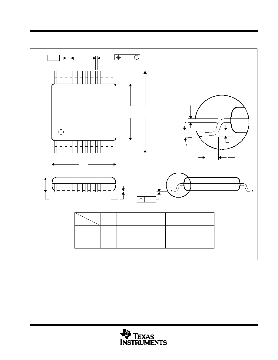
MECHANICAL DATA
MPDS006C ≠ FEBRUARY 1996 ≠ REVISED AUGUST 2000
POST OFFICE BOX 655303
∑
DALLAS, TEXAS 75265
DGV (R-PDSO-G**)
PLASTIC SMALL-OUTLINE
24 PINS SHOWN
14
3,70
3,50
4,90
5,10
20
DIM
PINS **
4073251/E 08/00
1,20 MAX
Seating Plane
0,05
0,15
0,25
0,50
0,75
0,23
0,13
1
12
24
13
4,30
4,50
0,16 NOM
Gage Plane
A
7,90
7,70
38
24
16
4,90
5,10
3,70
3,50
A MAX
A MIN
6,60
6,20
11,20
11,40
56
9,60
9,80
48
0,08
M
0,07
0,40
0
∞
≠ 8
∞
NOTES: A. All linear dimensions are in millimeters.
B. This drawing is subject to change without notice.
C. Body dimensions do not include mold flash or protrusion, not to exceed 0,15 per side.
D. Falls within JEDEC: 24/48 Pins ≠ MO-153
14/16/20/56 Pins ≠ MO-194
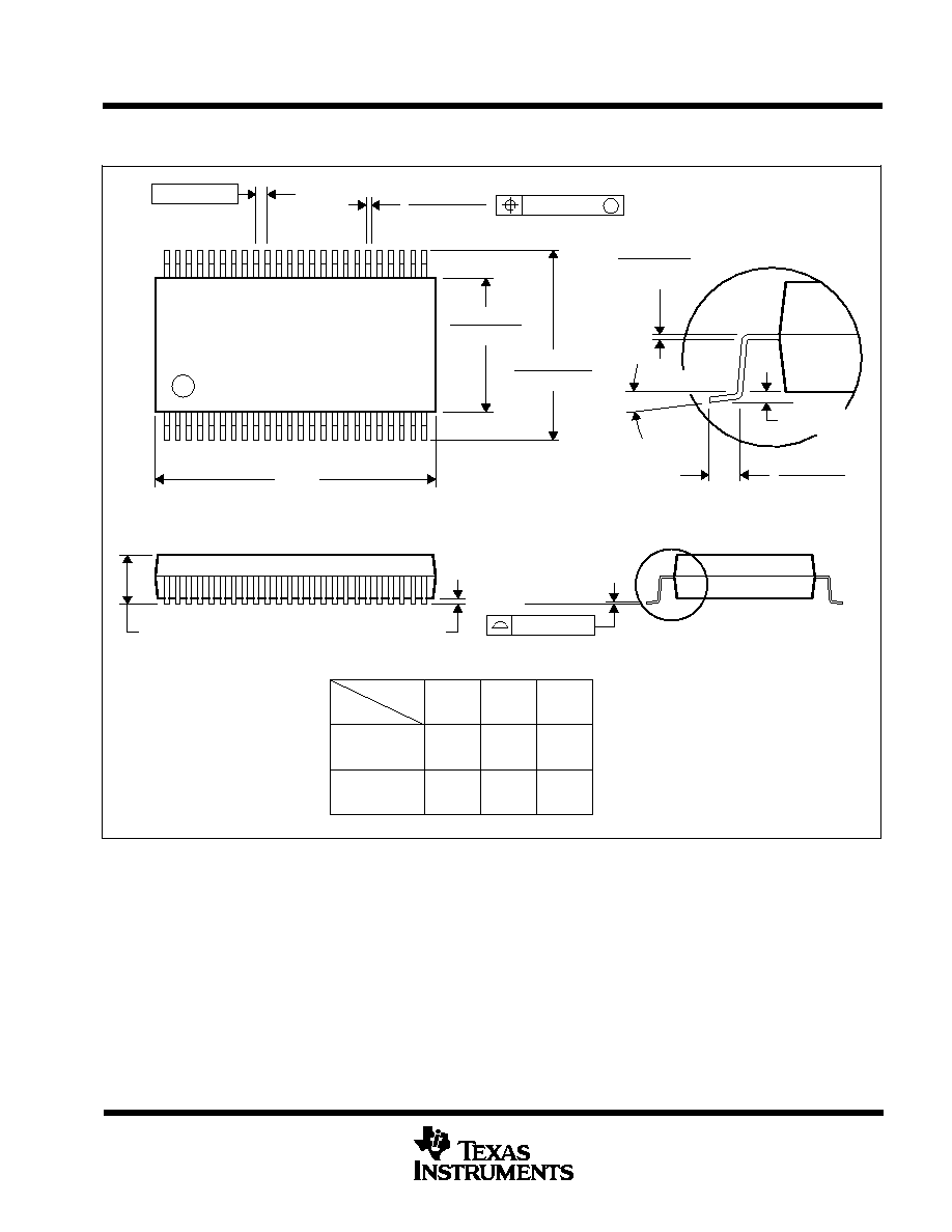
MECHANICAL DATA
MSSO001C ≠ JANUARY 1995 ≠ REVISED DECEMBER 2001
POST OFFICE BOX 655303
∑
DALLAS, TEXAS 75265
DL (R-PDSO-G**)
PLASTIC SMALL-OUTLINE PACKAGE
4040048 / E 12/01
48 PINS SHOWN
56
0.730
(18,54)
0.720
(18,29)
48
28
0.370
(9,40)
(9,65)
0.380
Gage Plane
DIM
0.420 (10,67)
0.395 (10,03)
A MIN
A MAX
0.010 (0,25)
PINS **
0.630
(16,00)
(15,75)
0.620
0.010 (0,25)
Seating Plane
0.020 (0,51)
0.040 (1,02)
25
24
0.008 (0,203)
0.0135 (0,343)
48
1
0.008 (0,20) MIN
A
0.110 (2,79) MAX
0.299 (7,59)
0.291 (7,39)
0.004 (0,10)
M
0.005 (0,13)
0.025 (0,635)
0
∞
≠ 8
∞
0.005 (0,13)
NOTES: A. All linear dimensions are in inches (millimeters).
B. This drawing is subject to change without notice.
C. Body dimensions do not include mold flash or protrusion not to exceed 0.006 (0,15).
D. Falls within JEDEC MO-118
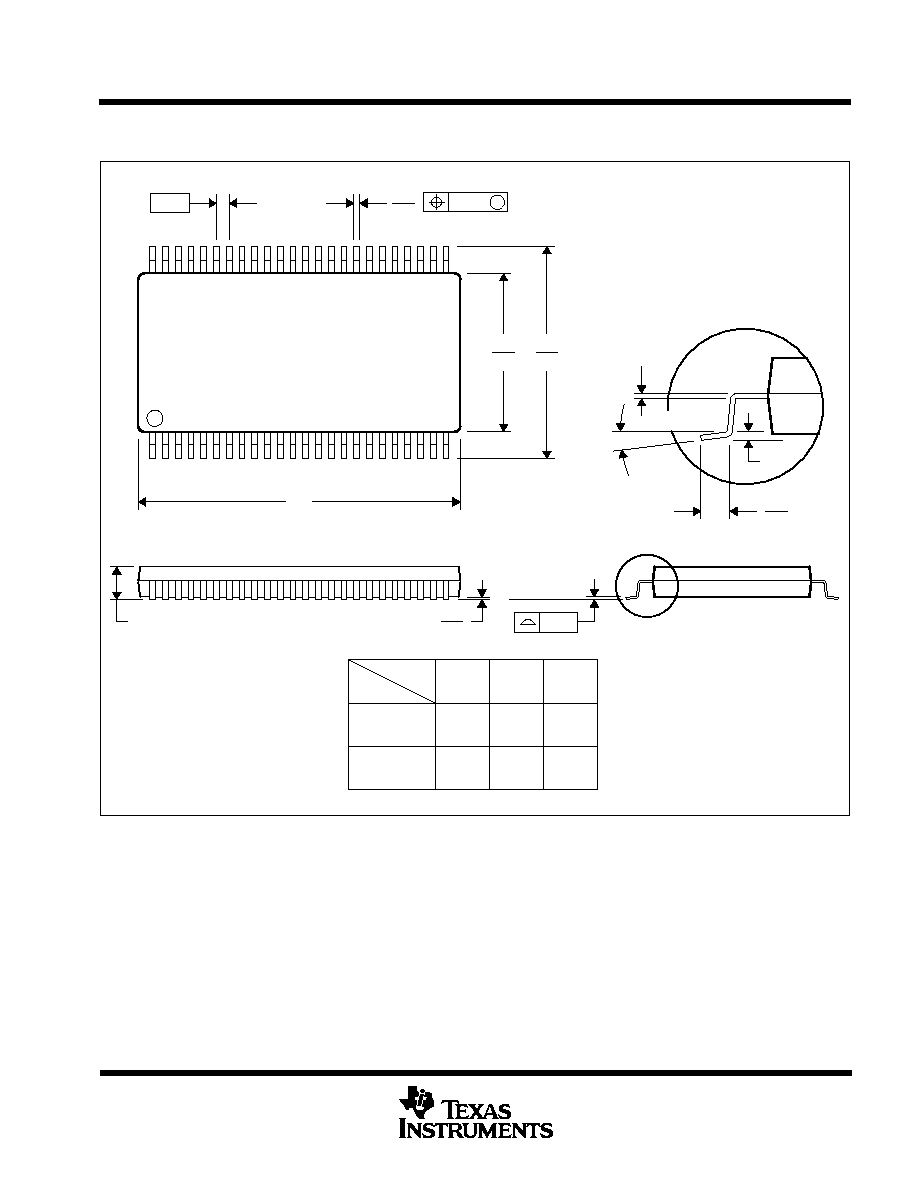
MECHANICAL DATA
MTSS003D ≠ JANUARY 1995 ≠ REVISED JANUARY 1998
POST OFFICE BOX 655303
∑
DALLAS, TEXAS 75265
DGG (R-PDSO-G**)
PLASTIC SMALL-OUTLINE PACKAGE
4040078 / F 12/97
48 PINS SHOWN
0,25
0,15 NOM
Gage Plane
6,00
6,20
8,30
7,90
0,75
0,50
Seating Plane
25
0,27
0,17
24
A
48
1
1,20 MAX
M
0,08
0,10
0,50
0
∞
≠ 8
∞
56
14,10
13,90
48
DIM
A MAX
A MIN
PINS **
12,40
12,60
64
17,10
16,90
0,15
0,05
NOTES: A. All linear dimensions are in millimeters.
B. This drawing is subject to change without notice.
C. Body dimensions do not include mold protrusion not to exceed 0,15.
D. Falls within JEDEC MO-153

IMPORTANT NOTICE
Texas Instruments Incorporated and its subsidiaries (TI) reserve the right to make corrections, modifications,
enhancements, improvements, and other changes to its products and services at any time and to discontinue
any product or service without notice. Customers should obtain the latest relevant information before placing
orders and should verify that such information is current and complete. All products are sold subject to TI's terms
and conditions of sale supplied at the time of order acknowledgment.
TI warrants performance of its hardware products to the specifications applicable at the time of sale in
accordance with TI's standard warranty. Testing and other quality control techniques are used to the extent TI
deems necessary to support this warranty. Except where mandated by government requirements, testing of all
parameters of each product is not necessarily performed.
TI assumes no liability for applications assistance or customer product design. Customers are responsible for
their products and applications using TI components. To minimize the risks associated with customer products
and applications, customers should provide adequate design and operating safeguards.
TI does not warrant or represent that any license, either express or implied, is granted under any TI patent right,
copyright, mask work right, or other TI intellectual property right relating to any combination, machine, or process
in which TI products or services are used. Information published by TI regarding third-party products or services
does not constitute a license from TI to use such products or services or a warranty or endorsement thereof.
Use of such information may require a license from a third party under the patents or other intellectual property
of the third party, or a license from TI under the patents or other intellectual property of TI.
Reproduction of information in TI data books or data sheets is permissible only if reproduction is without
alteration and is accompanied by all associated warranties, conditions, limitations, and notices. Reproduction
of this information with alteration is an unfair and deceptive business practice. TI is not responsible or liable for
such altered documentation.
Resale of TI products or services with statements different from or beyond the parameters stated by TI for that
product or service voids all express and any implied warranties for the associated TI product or service and
is an unfair and deceptive business practice. TI is not responsible or liable for any such statements.
Following are URLs where you can obtain information on other Texas Instruments products and application
solutions:
Products
Applications
Amplifiers
amplifier.ti.com
Audio
www.ti.com/audio
Data Converters
dataconverter.ti.com
Automotive
www.ti.com/automotive
DSP
dsp.ti.com
Broadband
www.ti.com/broadband
Interface
interface.ti.com
Digital Control
www.ti.com/digitalcontrol
Logic
logic.ti.com
Military
www.ti.com/military
Power Mgmt
power.ti.com
Optical Networking
www.ti.com/opticalnetwork
Microcontrollers
microcontroller.ti.com
Security
www.ti.com/security
Telephony
www.ti.com/telephony
Video & Imaging
www.ti.com/video
Wireless
www.ti.com/wireless
Mailing Address:
Texas Instruments
Post Office Box 655303 Dallas, Texas 75265
Copyright
2005, Texas Instruments Incorporated