74AC11244
OCTAL BUFFER/DRIVER
WITH 3-STATE OUTPUTS
SCAS171B ≠ MARCH 1987 ≠ REVISED SEPTEMBER 1998
1
POST OFFICE BOX 655303
∑
DALLAS, TEXAS 75265
D
EPIC
TM
(Enhanced-Performance Implanted
CMOS ) 1-
µ
m Process
D
3-State Outputs Drive Bus Lines or Buffer
Memory Address Registers
D
Flow-Through Architecture Optimizes PCB
Layout
D
Center-Pin V
CC
and GND Pin
Configurations Minimize High-Speed
Switching Noise
D
500-mA Typical Latch-Up Immunity at
125
∞
C
D
Package Options Include Plastic
Small-Outline (DW), Shrink Small-Outline
(DB), and Thin Shrink Small-Outline (PW)
Packages, and Standard Plastic DIPs (NT)
description
The 74AC11244 is an octal buffer or line driver designed specifically to improve both the performance and
density of 3-state memory address drivers, clock drivers, and bus-oriented receivers and transmitters. The
device can be used as two 4-bit buffers or one 8-bit buffer, with active-low output-enable (OE) inputs.
When OE is low, the device passes noninverted data from the A inputs to the Y outputs. When OE is high, the
outputs are in the high-impedance state.
To ensure the high-impedance state during power up or power down, OE should be tied to V
CC
through a pullup
resistor; the minimum value of the resistor is determined by the current-sinking capability of the driver.
The 74AC11244 is characterized for operation from ≠40
∞
C to 85
∞
C.
FUNCTION TABLE
(each driver)
INPUTS
OUTPUT
OE
A
Y
L
H
H
L
L
L
H
X
Z
Copyright
©
1998, Texas Instruments Incorporated
PRODUCTION DATA information is current as of publication date.
Products conform to specifications per the terms of Texas Instruments
standard warranty. Production processing does not necessarily include
testing of all parameters.
Please be aware that an important notice concerning availability, standard warranty, and use in critical applications of
Texas Instruments semiconductor products and disclaimers thereto appears at the end of this data sheet.
EPIC is a trademark of Texas Instruments Incorporated.
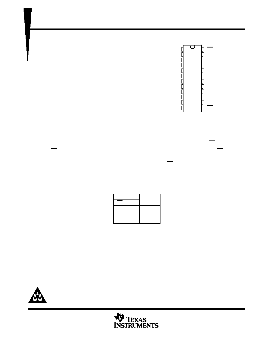
1
2
3
4
5
6
7
8
9
10
11
12
24
23
22
21
20
19
18
17
16
15
14
13
1Y1
1Y2
1Y3
1Y4
GND
GND
GND
GND
2Y1
2Y2
2Y3
2Y4
1OE
1A1
1A2
1A3
1A4
V
CC
V
CC
2A1
2A2
2A3
2A4
2OE
DB, DW, NT, OR PW PACKAGE
(TOP VIEW)
74AC11244
OCTAL BUFFER/DRIVER
WITH 3-STATE OUTPUTS
SCAS171B ≠ MARCH 1987 ≠ REVISED SEPTEMBER 1998
2
POST OFFICE BOX 655303
∑
DALLAS, TEXAS 75265
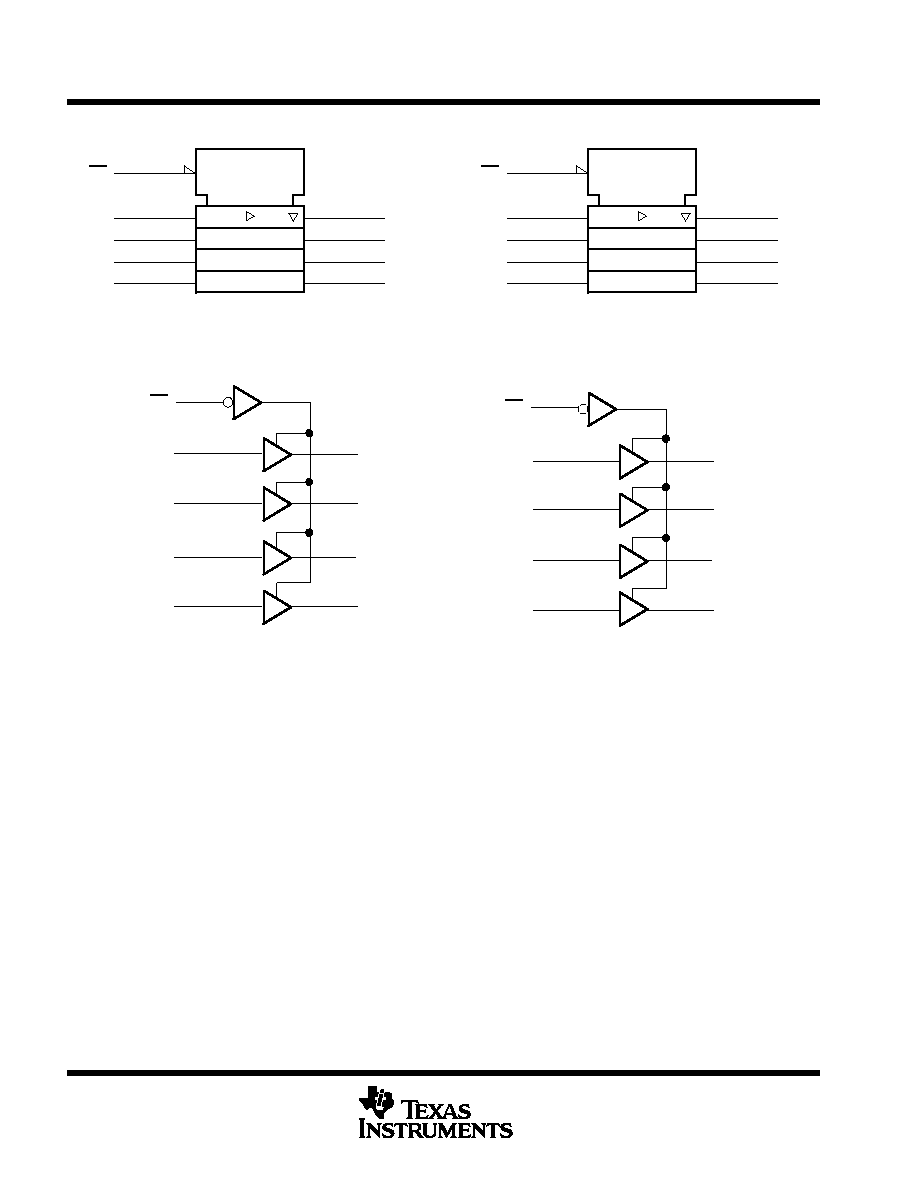
logic symbol
1OE
23
1A1
22
1A2
21
1A3
20
1A4
EN
24
1Y1
1
1Y2
2
1Y3
3
1Y4
4
2OE
17
2A1
16
2A2
15
2A3
14
2A4
EN
13
2Y1
9
2Y2
10
2Y3
11
2Y4
12
This symbol is in accordance with ANSI/IEEE Std 91-1984 and IEC Publication 617-12.
logic diagram (positive logic)
24
23
22
21
20
13
17
16
15
14
12
11
10
9
4
3
2
1
1A1
1A2
1A3
1A4
1Y1
2A1
2A2
2A3
2A4
2Y1
1Y2
1Y3
1Y4
2Y2
2Y3
2Y4
1OE
2OE
absolute maximum ratings over operating free-air temperature range (unless otherwise noted)
Supply voltage range, V
CC
≠0.5 V to 7 V
. . . . . . . . . . . . . . . . . . . . . . . . . . . . . . . . . . . . . . . . . . . . . . . . . . . . . . . . . .
Input voltage range, V
I
(see Note 1)
≠0.5 V to V
CC
+ 0.5 V
. . . . . . . . . . . . . . . . . . . . . . . . . . . . . . . . . . . . . . . . . . .
Output voltage range, V
O
(see Note 1)
≠0.5 V to V
CC
+ 0.5 V
. . . . . . . . . . . . . . . . . . . . . . . . . . . . . . . . . . . . . . . .
Input clamp current, I
IK
(V
I
< 0 or V
I
> V
CC
)
±
20 mA
. . . . . . . . . . . . . . . . . . . . . . . . . . . . . . . . . . . . . . . . . . . . . . . .
Output clamp current, I
OK
(V
O
< 0 or V
O
> V
CC
)
±
50 mA
. . . . . . . . . . . . . . . . . . . . . . . . . . . . . . . . . . . . . . . . . . . .
Continuous output current, I
O
(V
O
= 0 to V
CC
)
±
50 mA
. . . . . . . . . . . . . . . . . . . . . . . . . . . . . . . . . . . . . . . . . . . . . .
Continuous current through V
CC
or GND
±
200 mA
. . . . . . . . . . . . . . . . . . . . . . . . . . . . . . . . . . . . . . . . . . . . . . . . . .
Package thermal impedance,
JA
(see Note 2): DB package
104
∞
C/W
. . . . . . . . . . . . . . . . . . . . . . . . . . . . . . . .
DW package
81
∞
C/W
. . . . . . . . . . . . . . . . . . . . . . . . . . . . . . . . .
PW package
120
∞
C/W
. . . . . . . . . . . . . . . . . . . . . . . . . . . . . . . .
NT package
67
∞
C/W
. . . . . . . . . . . . . . . . . . . . . . . . . . . . . . . . .
Storage temperature range, T
stg
≠65
∞
C to 150
∞
C
. . . . . . . . . . . . . . . . . . . . . . . . . . . . . . . . . . . . . . . . . . . . . . . . . . .
Stresses beyond those listed under "absolute maximum ratings" may cause permanent damage to the device. These are stress ratings only, and
functional operation of the device at these or any other conditions beyond those indicated under "recommended operating conditions" is not
implied. Exposure to absolute-maximum-rated conditions for extended periods may affect device reliability.
NOTES:
1. The input and output voltage ratings may be exceeded if the input and output current ratings are observed.
2. The package thermal impedance is calculated in accordance with JESD 51, except for through-hole packages, which use a trace
length of zero.
74AC11244
OCTAL BUFFER/DRIVER
WITH 3-STATE OUTPUTS
SCAS171B ≠ MARCH 1987 ≠ REVISED SEPTEMBER 1998
3
POST OFFICE BOX 655303
∑
DALLAS, TEXAS 75265
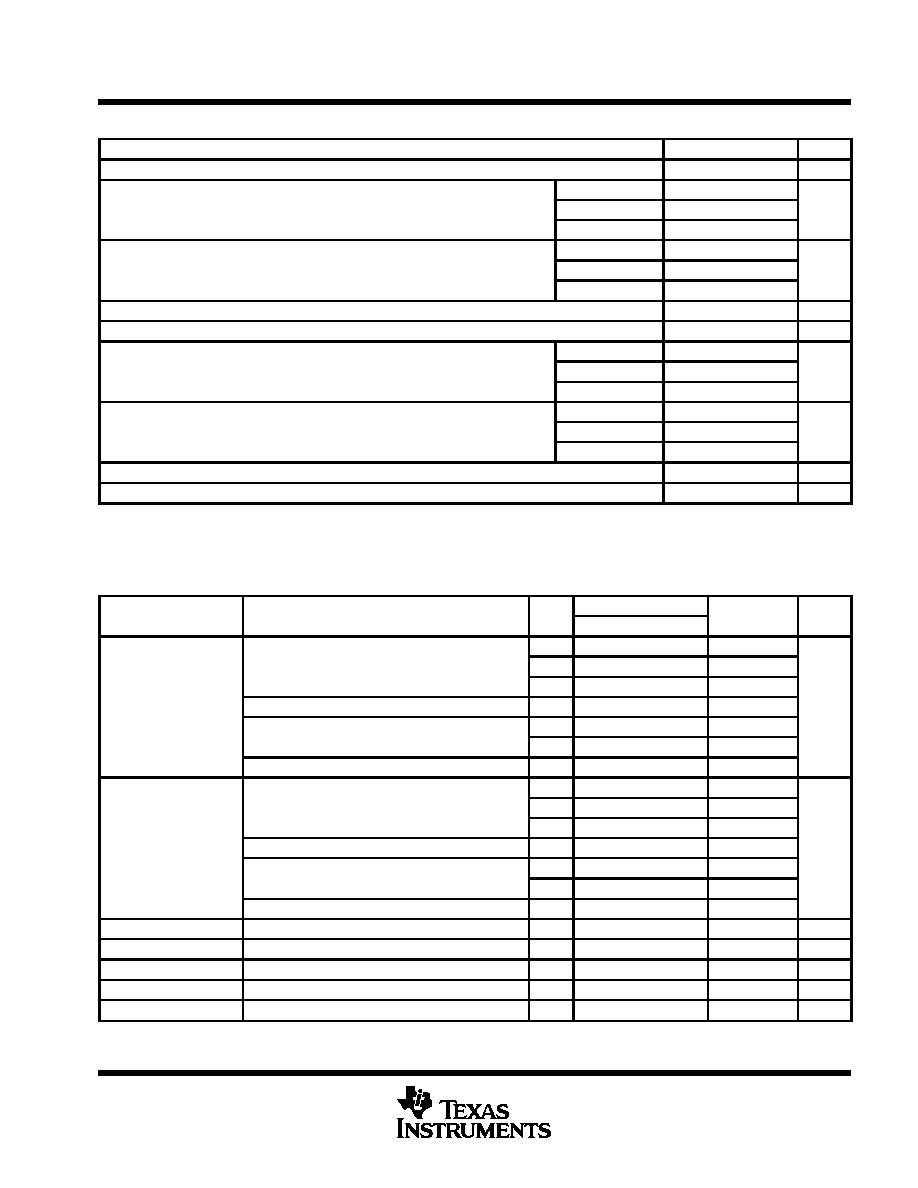
recommended operating conditions (see Note 3)
MIN
NOM
MAX
UNIT
VCC
Supply voltage
3
5
5.5
V
VCC = 3 V
2.1
VIH
High-level input voltage
VCC = 4.5 V
3.15
V
VCC = 5.5 V
3.85
VCC = 3 V
0.9
VIL
Low-level input voltage
VCC = 4.5 V
1.35
V
VCC = 5.5 V
1.65
VI
Input voltage
0
VCC
V
VO
Output voltage
0
VCC
V
VCC = 3 V
≠4
IOH
High-level output current
VCC = 4.5 V
≠24
mA
VCC = 5.5 V
≠24
VCC = 3 V
12
IOL
Low-level output current
VCC = 4.5 V
24
mA
VCC = 5.5 V
24
t/
v
Input transition rise or fall rate
0
10
ns/V
TA
Operating free-air temperature
≠40
85
∞
C
NOTE 3: All unused inputs of the device must be held at VCC or GND to ensure proper device operation. Refer to the TI application report,
Implications of Slow or Floating CMOS Inputs, literature number SCBA004.
electrical characteristics over recommended operating free-air temperature range (unless
otherwise noted)
PARAMETER
TEST CONDITIONS
VCC
TA = 25
∞
C
MIN
MAX
UNIT
PARAMETER
TEST CONDITIONS
VCC
MIN
TYP
MAX
MIN
MAX
UNIT
3 V
2.9
2.9
IOH = ≠50
µ
A
4.5 V
4.4
4.4
5.5 V
5.4
5.4
VOH
IOH = ≠4 mA
3 V
2.58
2.48
V
I
24
A
4.5 V
3.94
3.8
IOL = ≠24 mA
5.5 V
4.94
4.8
IOH = ≠75 mA
5.5 V
3.85
3 V
0.1
0.1
IOL = 50
µ
A
4.5 V
0.1
0.1
5.5 V
0.1
0.1
VOL
IOL = 12 mA
3 V
0.36
0.44
V
IOL = 24 mA
4.5 V
0.36
0.44
IOL = 24 mA
5.5 V
0.36
0.44
IOL = 75 mA
5.5 V
1.65
II
VI = VCC or GND
5.5 V
±
0.1
±
1
µ
A
IOZ
VO = VCC or GND
5.5 V
±
0.5
±
5
µ
A
ICC
VI = VCC or GND,
IO = 0
5.5 V
8
80
µ
A
Ci
VI = VCC or GND
5 V
4
pF
Co
VO = VCC or GND
5 V
10
pF
Not more than one output should be tested at a time, and the duration of the test should not exceed 10 ms.
74AC11244
OCTAL BUFFER/DRIVER
WITH 3-STATE OUTPUTS
SCAS171B ≠ MARCH 1987 ≠ REVISED SEPTEMBER 1998
4
POST OFFICE BOX 655303
∑
DALLAS, TEXAS 75265
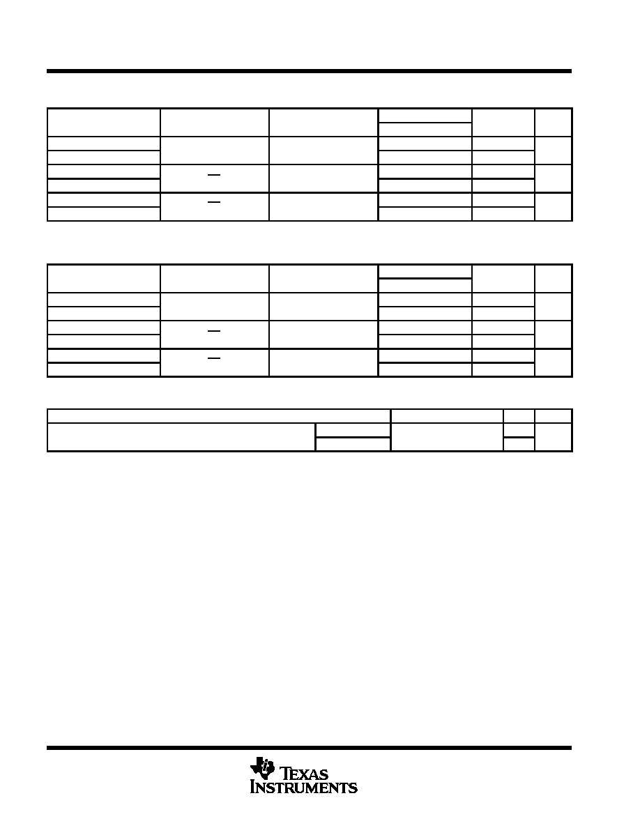
switching characteristics over recommended operating free-air temperature range,
V
CC
= 3.3 V
±
0.3 V (unless otherwise noted) (see Figure 1)
PARAMETER
FROM
TO
TA = 25
∞
C
MIN
MAX
UNIT
PARAMETER
(INPUT)
(OUTPUT)
MIN
TYP
MAX
MIN
MAX
UNIT
tPLH
A
Y
1.5
7.1
9.3
1.5
10.2
ns
tPHL
A
Y
1.5
6.3
8.6
1.5
9.5
ns
tPZH
OE
Y
1.5
8
10.7
1.5
11.8
ns
tPZL
OE
Y
1.5
7.9
10.6
1.5
11.9
ns
tPHZ
OE
Y
1.5
5.9
7.9
1.5
8.3
ns
tPLZ
OE
Y
1.5
7.2
9.4
1.5
9.9
ns
switching characteristics over recommended operating free-air temperature range,
V
CC
= 5 V
±
0.5 V (unless otherwise noted) (see Figure 1)
PARAMETER
FROM
TO
TA = 25
∞
C
MIN
MAX
UNIT
PARAMETER
(INPUT)
(OUTPUT)
MIN
TYP
MAX
MIN
MAX
UNIT
tPLH
A
Y
1.5
4.9
6.7
1.5
7.3
ns
tPHL
A
Y
1.5
4.5
6.4
1.5
6.9
ns
tPZH
OE
Y
1.5
5.4
7.7
1.5
8.5
ns
tPZL
OE
Y
1.5
5.4
7.6
1.5
8.5
ns
tPHZ
OE
Y
1.5
5.2
7
1.5
7.3
ns
tPLZ
OE
Y
1.5
5.8
7.8
1.5
8.2
ns
operating characteristics, V
CC
= 5 V, T
A
= 25
∞
C
PARAMETER
TEST CONDITIONS
TYP
UNIT
C d
Power dissipation capacitance per buffer/driver
Outputs enabled
CL = 50 pF
f = 1 MHz
27
pF
Cpd
Power dissipation capacitance per buffer/driver
Outputs disabled
CL = 50 pF,
f = 1 MHz
9
pF
74AC11244
OCTAL BUFFER/DRIVER
WITH 3-STATE OUTPUTS
SCAS171B ≠ MARCH 1987 ≠ REVISED SEPTEMBER 1998
5
POST OFFICE BOX 655303
∑
DALLAS, TEXAS 75265
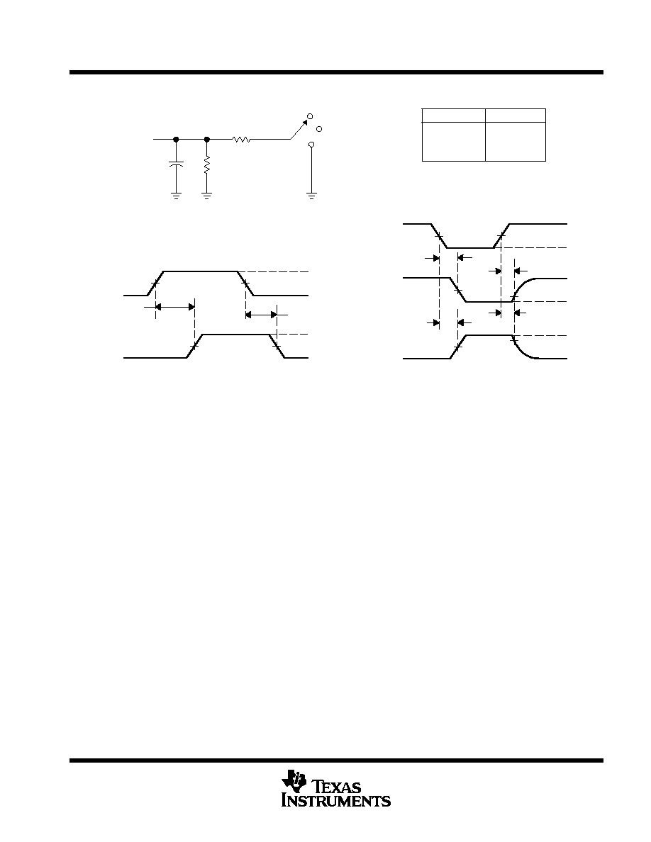
PARAMETER MEASUREMENT INFORMATION
From Output
Under Test
CL = 50 pF
(see Note A)
LOAD CIRCUIT
S1
2
◊
VCC
500
500
tPLH
tPHL
Output
Control
(low-level
enabling)
Output
Waveform 1
S1 at 2
◊
VCC
(see Note B)
Output
Waveform 2
S1 at GND
(see Note B)
VOL
VOH
tPZL
tPZH
tPLZ
tPHZ
50%
50%
50%
50%
[
VCC
VCC
0 V
50% VCC
50% VCC
VOH
VOL
0 V
50% VCC
20% VCC
50% VCC
80% VCC
[
0 V
VCC
GND
Open
Input
Output
VOLTAGE WAVEFORMS
VOLTAGE WAVEFORMS
tPLH/tPHL
tPLZ/tPZL
tPHZ/tPZH
Open
2
◊
VCC
GND
TEST
S1
NOTES: A. CL includes probe and jig capacitance.
B. Waveform 1 is for an output with internal conditions such that the output is low except when disabled by the output control.
Waveform 2 is for an output with internal conditions such that the output is high except when disabled by the output control.
C. All input pulses are supplied by generators having the following characteristics: PRR
1 MHz, ZO = 50
, tr = 3 ns, tf = 3 ns.
D. The outputs are measured one at a time with one input transition per measurement.
Figure 1. Load Circuit and Voltage Waveforms

IMPORTANT NOTICE
Texas Instruments and its subsidiaries (TI) reserve the right to make changes to their products or to discontinue
any product or service without notice, and advise customers to obtain the latest version of relevant information
to verify, before placing orders, that information being relied on is current and complete. All products are sold
subject to the terms and conditions of sale supplied at the time of order acknowledgement, including those
pertaining to warranty, patent infringement, and limitation of liability.
TI warrants performance of its semiconductor products to the specifications applicable at the time of sale in
accordance with TI's standard warranty. Testing and other quality control techniques are utilized to the extent
TI deems necessary to support this warranty. Specific testing of all parameters of each device is not necessarily
performed, except those mandated by government requirements.
CERTAIN APPLICATIONS USING SEMICONDUCTOR PRODUCTS MAY INVOLVE POTENTIAL RISKS OF
DEATH, PERSONAL INJURY, OR SEVERE PROPERTY OR ENVIRONMENTAL DAMAGE ("CRITICAL
APPLICATIONS"). TI SEMICONDUCTOR PRODUCTS ARE NOT DESIGNED, AUTHORIZED, OR
WARRANTED TO BE SUITABLE FOR USE IN LIFE-SUPPORT DEVICES OR SYSTEMS OR OTHER
CRITICAL APPLICATIONS. INCLUSION OF TI PRODUCTS IN SUCH APPLICATIONS IS UNDERSTOOD TO
BE FULLY AT THE CUSTOMER'S RISK.
In order to minimize risks associated with the customer's applications, adequate design and operating
safeguards must be provided by the customer to minimize inherent or procedural hazards.
TI assumes no liability for applications assistance or customer product design. TI does not warrant or represent
that any license, either express or implied, is granted under any patent right, copyright, mask work right, or other
intellectual property right of TI covering or relating to any combination, machine, or process in which such
semiconductor products or services might be or are used. TI's publication of information regarding any third
party's products or services does not constitute TI's approval, warranty or endorsement thereof.
Copyright
©
1998, Texas Instruments Incorporated