
54AC16472, 74AC16472
18-BIT REGISTERED TRANSCIEVERS
WITH 3-STATE OUTPUTS
SCAS165A ≠ JUNE 1990 ≠ REVISED APRIL 1996
1
POST OFFICE BOX 655303
∑
DALLAS, TEXAS 75265
D
Members of the Texas Instruments
Widebus
TM
Family
D
3-State True Outputs
D
Flow-Through Architecture Optimizes
PCB Layout
D
Distributed V
CC
and GND Pin Configuration
Minimizes High-Speed Switching Noise
D
EPIC
TM
(Enhanced-Performance Implanted
CMOS) 1-
µ
m Process
D
500-mA Typical Latch-Up Immunity at
125
∞
C
D
Package Options Include Plastic 300-mil
Shrink Small-Outline (DL) Package Using
25-mil Center-to-Center Pin Spacings and
380-mil Fine-Pitch Ceramic Flat (WD)
Package Using 25-mil Center-to-Center Pin
Spacings
description
The 'AC16472 are 18-bit registered transceivers
that contain two sets of D-type latches for
temporary storage of data flowing in either
direction. They can be used as two 9-bit
transceivers or one 18-bit transceiver. Separate
latch-enable (LEAB or LEBA) and output-enable
(OEAB or OEBA) inputs are provided for each
register to permit independent control in either
direction of data flow.
When OEAB and LEAB are both low, the A-to-B
latches are transparent; a subsequent low-to-high
transition of LEAB puts the A latches in the
storage mode. With OEAB low, the B outputs are active and reflect the data present at the output of the A latches.
Data flow from B to A is similar, but requires the use of the LEBA and OEBA inputs.
The 74AC16472 is packaged in TI's shrink small-outline package (DL), which provides twice the I/O pin count
and functionality of standard small-outline packages in the same printed-circuit-board area.
The 54AC16472 is characterized for operation over the full military temperature range of ≠55
∞
C to 125
∞
C. The
74AC16472 is characterized for operation from ≠40
∞
C to 85
∞
C.
Copyright
©
1996, Texas Instruments Incorporated
UNLESS OTHERWISE NOTED this document contains PRODUCTION
DATA information current as of publication date. Products conform to
specifications per the terms of Texas Instruments standard warranty.
Production processing does not necessarily include testing of all
parameters.
EPIC and Widebus are trademarks of Texas Instruments Incorporated.
1
2
3
4
5
6
7
8
9
10
11
12
13
14
15
16
17
18
19
20
21
22
23
24
25
26
27
28
56
55
54
53
52
51
50
49
48
47
46
45
44
43
42
41
40
39
38
37
36
35
34
33
32
31
30
29
1OEAB
1LEAB
1A1
GND
1A2
1A3
V
CC
1A4
1A5
1A6
GND
1A7
1A8
1A9
2A1
2A2
2A3
GND
2A4
2A5
2A6
V
CC
2A7
2A8
GND
2A9
2LEAB
2OEAB
1OEBA
1LEBA
1B1
GND
1B2
1B3
V
CC
1B4
1B5
1B6
GND
1B7
1B8
1B9
2B1
2B2
2B3
GND
2B4
2B5
2B6
V
CC
2B7
2B8
GND
2B9
2LEBA
2OEBA
54AC16472 . . . WD PACKAGE
74AC16472 . . . DL PACKAGE
(TOP VIEW)
Please be aware that an important notice concerning availability, standard warranty, and use in critical applications of
Texas Instruments semiconductor products and disclaimers thereto appears at the end of this data sheet.
54AC16472, 74AC16472
18-BIT REGISTERED TRANSCIEVERS
WITH 3-STATE OUTPUTS
SCAS165A ≠ JUNE 1990 ≠ REVISED APRIL 1996
2
POST OFFICE BOX 655303
∑
DALLAS, TEXAS 75265
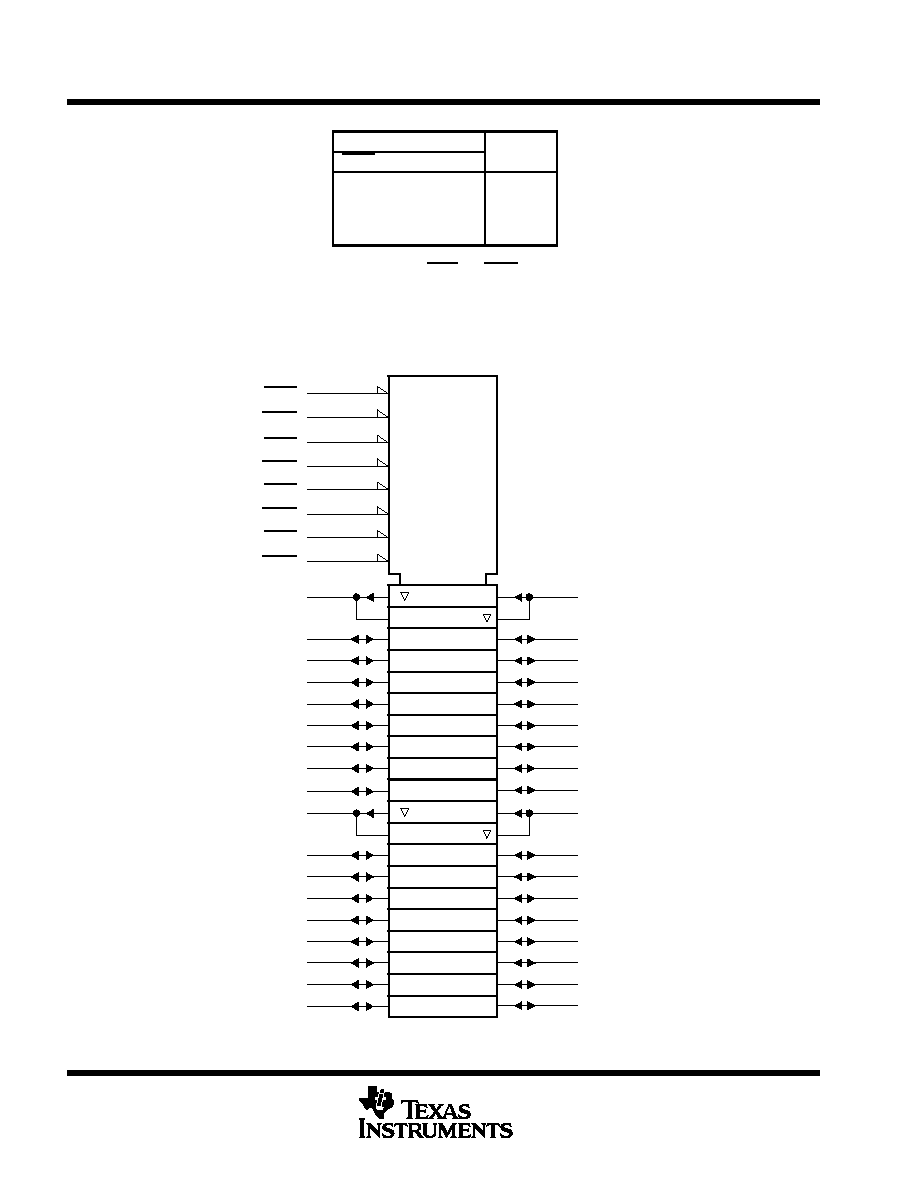
FUNCTION TABLE
INPUTS
OUTPUT
LEAB
OEAB
A
B
X
H
X
Z
H
L
X
B0
L
L
H
H
L
L
L
L
A-to-B data flow is shown: B-to-A flow is
similar but uses LEBA and OEBA.
Output level before the indicated
steady-state input conditions were
established
logic symbol
ß
1OEBA
1A1
3
4
1D
1A2
5
1A3
6
1A4
8
1A5
9
1A6
10
1A7
12
1A8
13
1B1
54
3D
1B2
52
1B3
51
1B4
49
1B5
48
1B6
47
1B7
45
1B8
44
1
2A1
15
8
5D
2A2
16
2A3
17
2A4
19
2A5
20
2A6
21
2A7
23
2A8
24
2B1
42
7D
2B2
41
2B3
40
2B4
38
2B5
37
2B6
36
2B7
34
2B8
33
1
1
1
C1
2
EN2
1
C3
55
EN4
56
C5
27
EN6
28
C7
30
EN8
29
1LEBA
1OEAB
1LEAB
2OEBA
2LEBA
2OEAB
2LEAB
1B9
43
1A9
14
6
2A9
26
2B9
31
2
ß This symbol is in accordance with ANSI/IEEE Std 91-1984 and IEC Publication 617-12.
54AC16472, 74AC16472
18-BIT REGISTERED TRANSCIEVERS
WITH 3-STATE OUTPUTS
SCAS165A ≠ JUNE 1990 ≠ REVISED APRIL 1996
3
POST OFFICE BOX 655303
∑
DALLAS, TEXAS 75265
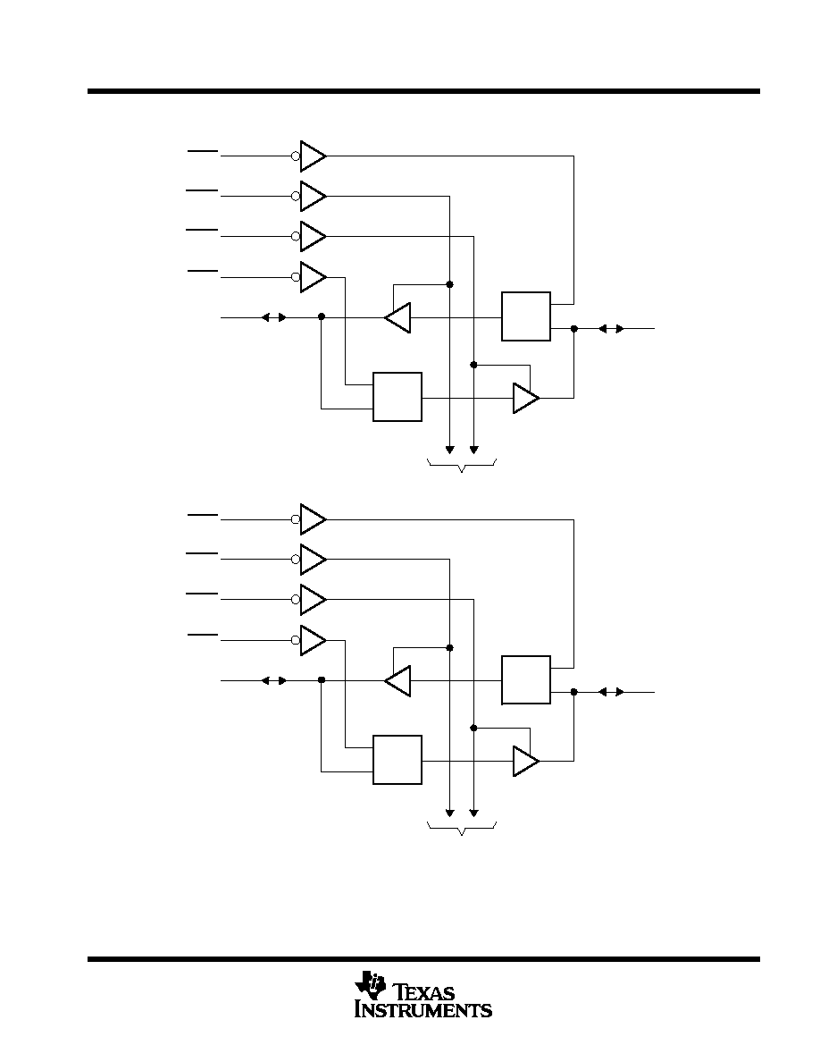
logic diagram (positive logic)
1OEBA
1LEBA
1OEAB
1LEAB
1A1
1B1
56
To Eight Other Channels
C1
1D
C1
1D
1
2
3
55
54
2OEBA
2LEBA
2OEAB
2LEAB
2A1
2B1
29
To Eight Other Channels
C1
1D
C1
1D
28
27
15
30
42
54AC16472, 74AC16472
18-BIT REGISTERED TRANSCIEVERS
WITH 3-STATE OUTPUTS
SCAS165A ≠ JUNE 1990 ≠ REVISED APRIL 1996
4
POST OFFICE BOX 655303
∑
DALLAS, TEXAS 75265
absolute maximum ratings over operating free-air temperature range (unless otherwise noted)
Supply voltage range, V
CC
≠0.5 V to 7 V
. . . . . . . . . . . . . . . . . . . . . . . . . . . . . . . . . . . . . . . . . . . . . . . . . . . . . . . . . .
Input voltage range, V
I
(see Note 1)
≠0.5 V to V
CC
+ 0.5 V
. . . . . . . . . . . . . . . . . . . . . . . . . . . . . . . . . . . . . . . . . . .
Output voltage range, V
O
(see Note 1)
≠0.5 V to V
CC
+ 0.5 V
. . . . . . . . . . . . . . . . . . . . . . . . . . . . . . . . . . . . . . . .
Input clamp current, I
IK
(V
I
< 0 or V
I
> V
CC
)
±
20 mA
. . . . . . . . . . . . . . . . . . . . . . . . . . . . . . . . . . . . . . . . . . . . . . . .
Output clamp current, I
OK
(V
O
< 0 or V
O
> V
CC
)
±
50 mA
. . . . . . . . . . . . . . . . . . . . . . . . . . . . . . . . . . . . . . . . . . . .
Continuous output current, I
O
(V
O
= 0 to V
CC
)
±
50 mA
. . . . . . . . . . . . . . . . . . . . . . . . . . . . . . . . . . . . . . . . . . . . . .
Continuous current through V
CC
or GND
±
450 mA
. . . . . . . . . . . . . . . . . . . . . . . . . . . . . . . . . . . . . . . . . . . . . . . . . .
Maximum power package dissipation at T
A
= 55
∞
C (in still air) (see Note 2): DL package
1.4 W
. . . . . . . . . .
Storage temperature range, T
stg
≠65
∞
C to 150
∞
C
. . . . . . . . . . . . . . . . . . . . . . . . . . . . . . . . . . . . . . . . . . . . . . . . . . .
Stresses beyond those listed under "absolute maximum ratings" may cause permanent damage to the device. These are stress ratings only, and
functional operation of the device at these or any other conditions beyond those indicated under "recommended operating conditions" is not
implied. Exposure to absolute-maximum-rated conditions for extended periods may affect device reliability.
NOTES:
1. The input and output voltage ratings may be exceeded if the input and output current ratings are observed.
2. The maximum package power dissipation is calculated using a junction temperature of 150
_
C and a board trace length of 750 mils.
recommended operating conditions (see Note 3)
54AC16472
74AC16472
UNIT
MIN
NOM
MAX
MIN
NOM
MAX
UNIT
VCC
Supply voltage
3
5
5.5
3
5
5.5
V
VCC = 3 V
2.1
2.1
VIH
High-level input voltage
VCC = 4.5 V
3.15
3.15
V
VCC = 5.5 V
3.85
3.85
VCC = 3 V
0.9
0.9
VIL
Low-level input voltage
VCC = 4.5 V
1.35
1.35
V
VCC = 5.5 V
1.65
1.65
VI
Input voltage
0
VCC
0
VCC
V
VO
Output voltage
0
VCC
0
VCC
V
VCC = 3 V
≠4
≠4
IOH
High-level output current
VCC = 4.5 V
≠24
≠24
mA
VCC = 5.5 V
≠24
≠24
VCC = 3 V
12
12
IOL
Low-level output current
VCC = 4.5 V
24
24
mA
VCC = 5.5 V
24
24
t/
v
Input transition rise or fall rate
0
10
0
10
ns/V
TA
Operating free-air temperature
≠55
125
≠40
85
∞
C
NOTE 3: Unused inputs must be held high or low to prevent them from floating.
PRODUCT PREVIEW information concerns products in the formative or
design phase of development. Characteristic data and other
specifications are design goals. Texas Instruments reserves the right to
change or discontinue these products without notice.
54AC16472, 74AC16472
18-BIT REGISTERED TRANSCIEVERS
WITH 3-STATE OUTPUTS
SCAS165A ≠ JUNE 1990 ≠ REVISED APRIL 1996
5
POST OFFICE BOX 655303
∑
DALLAS, TEXAS 75265
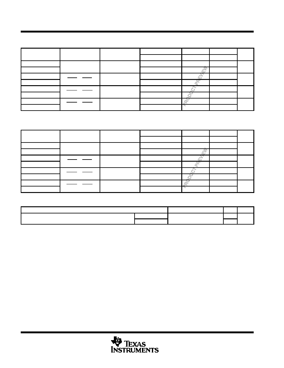
electrical characteristics over recommended operating free-air temperature range (unless
otherwise noted)
PARAMETER
TEST CONDITIONS
VCC
TA = 25
∞
C
54AC16472
74AC16472
UNIT
PARAMETER
TEST CONDITIONS
VCC
MIN
TYP
MAX
MIN
MAX
MIN
MAX
UNIT
3 V
2.9
2.9
2.9
IOH = ≠50
µ
A
4.5 V
4.4
4.4
4.4
5.5 V
5.4
5.4
5.4
VOH
IOH = ≠4 mA
3 V
2.58
2.48
2.48
V
I
24
A
4.5 V
3.94
3.8
3.8
IOL = ≠24 mA
5.5 V
4.94
4.8
4.8
IOH = ≠75 mA
5.5 V
3.85
3.85
3 V
0.1
0.1
0.1
IOL = 50
µ
A
4.5 V
0.1
0.1
0.1
5.5 V
0.1
0.1
0.1
VOL
IOL = 12 mA
3 V
0.36
0.44
0.44
V
IOL = 24 mA
4.5 V
0.36
0.44
0.44
IOL = 24 mA
5.5 V
0.36
0.44
0.44
IOL = 75 mA
5.5 V
1.65
1.65
II
Control inputs
VI = VCC or GND
5.5 V
±
0.1
±
1
±
1
µ
A
IOZ
A or B ports
VO = VCC or GND
5.5 V
±
0.5
±
5
±
5
µ
A
ICC
VI = VCC or GND,
IO = 0
5.5 V
8
80
80
µ
A
Ci
Control inputs
VI = VCC or GND
5 V
3
pF
Cio
A or B ports
VO = VCC or GND
5 V
11.5
pF
Not more than one output should be tested at a time, and the duration of the test should not exceed 10 ms.
For I/O ports, the parameter IOZ includes the input leakage current.
timing requirements over recommended operating free-air temperature range,
V
CC
= 3.3 V
±
0.3 V (unless otherwise noted) (see Figure 1)
TA = 25
∞
C
54AC16472
74AC16472
UNIT
MIN
MAX
MIN
MAX
MIN
MAX
UNIT
tw
Pulse duration, LEAB or LEBA low
4
4
4
ns
tsu
Setup time, data before LEAB or LEBA
0.5
0.5
0.5
ns
th
Hold time, data after LEAB or LEBA
3.5
3.5
3.5
ns
timing requirements over recommended operating free-air temperature range,
V
CC
= 5 V
±
0.5 V (unless otherwise noted) (see Figure 1)
TA = 25
∞
C
54AC16472
74AC16472
UNIT
MIN
MAX
MIN
MAX
MIN
MAX
UNIT
tw
Pulse duration, LEAB or LEBA low
4
4
4
ns
tsu
Setup time, data before LEAB or LEBA
0.5
0.5
0.5
ns
th
Hold time, data after LEAB or LEBA
2.5
2.5
2.5
ns
PRODUCT PREVIEW information concerns products in the formative or
design phase of development. Characteristic data and other
specifications are design goals. Texas Instruments reserves the right to
change or discontinue these products without notice.
54AC16472, 74AC16472
18-BIT REGISTERED TRANSCIEVERS
WITH 3-STATE OUTPUTS
SCAS165A ≠ JUNE 1990 ≠ REVISED APRIL 1996
6
POST OFFICE BOX 655303
∑
DALLAS, TEXAS 75265
switching characteristics over recommended operating free-air temperature range,
V
CC
= 3.3 V
±
0.3 V (unless otherwise noted) (see Figure 1)
PARAMETER
FROM
TO
TA = 25
∞
C
54AC16472
74AC16472
UNIT
PARAMETER
(INPUT)
(OUTPUT)
MIN
TYP
MAX
MIN
MAX
MIN
MAX
UNIT
tPLH
A or B
B or A
3.5
8
12.5
3.5
14.2
3.5
14.2
ns
tPHL
A or B
B or A
3.9
8.4
12.8
3.9
13.9
3.9
13.9
ns
tPLH
LEBA or LEAB
A or B
4.8
10.3
15.6
4.8
17.9
4.8
17.9
ns
tPHL
LEBA or LEAB
A or B
4.7
9.7
14.7
4.7
16.3
4.7
16.3
ns
tPZH
OEBA or OEAB
A or B
3.9
8.9
14
3.9
15.9
3.9
15.9
ns
tPZL
OEBA or OEAB
A or B
5
11.2
17.6
5
19.7
5
19.7
ns
tPHZ
OEBA or OEAB
A or B
4.4
7
9.4
4.4
10
4.4
10
ns
tPLZ
OEBA or OEAB
A or B
4
6.4
8.7
4
9.4
4
9.4
ns
switching characteristics over recommended operating free-air temperature range,
V
CC
= 5 V
±
0.5 V (unless otherwise noted) (see Figure 1)
PARAMETER
FROM
TO
TA = 25
∞
C
54AC16472
74AC16472
UNIT
PARAMETER
(INPUT)
(OUTPUT)
MIN
TYP
MAX
MIN
MAX
MIN
MAX
UNIT
tPLH
A or B
B or A
2.9
5.6
8.4
2.9
9.5
2.9
9.5
ns
tPHL
A or B
B or A
3.1
6
8.7
3.1
9.6
3.1
9.6
ns
tPLH
LEBA or LEAB
A or B
3.9
7.3
10.3
3.9
11.7
3.9
11.7
ns
tPHL
LEBA or LEAB
A or B
3.7
6.9
9.7
3.7
10.9
3.7
10.9
ns
tPZH
OEBA or OEAB
A or B
3.1
6.2
8.9
3.1
10.2
3.1
10.2
ns
tPZL
OEBA or OEAB
A or B
3.9
7.3
10.4
3.9
11.6
3.9
11.6
ns
tPHZ
OEBA or OEAB
A or B
4.3
6.2
8.1
4.3
8.6
4.3
8.6
ns
tPLZ
OEBA or OEAB
A or B
3.8
5.7
7.4
3.8
8
3.8
8
ns
operating characteristics, V
CC
= 5 V, T
A
= 25
∞
C
PARAMETER
TEST CONDITIONS
TYP
UNIT
Cpd
Power dissipation capacitance per transceiver
Outputs enabled
CL = 50 pF
f = 1 MHz
59
pF
Cpd
Power dissi ation ca acitance er transceiver
Outputs disabled
CL = 50 F, f = 1 MHz
6
F
PRODUCT PREVIEW information concerns products in the formative or
design phase of development. Characteristic data and other
specifications are design goals. Texas Instruments reserves the right to
change or discontinue these products without notice.

54AC16472, 74AC16472
18-BIT REGISTERED TRANSCIEVERS
WITH 3-STATE OUTPUTS
SCAS165A ≠ JUNE 1990 ≠ REVISED APRIL 1996
7
POST OFFICE BOX 655303
∑
DALLAS, TEXAS 75265
PARAMETER MEASUREMENT INFORMATION
50% VCC
50%
50%
50%
VCC
VCC
0 V
0 V
th
tsu
VOLTAGE WAVEFORMS
Data Input
tPLH
tPHL
tPHL
tPLH
VOH
VOH
VOL
VOL
50%
50%
VCC
0 V
50% VCC
50% VCC
Input
Out-of-Phase
Output
In-Phase
Output
Timing Input
50% VCC
VOLTAGE WAVEFORMS
From Output
Under Test
CL = 50 pF
(see Note A)
LOAD CIRCUIT
S1
2
◊
VCC
500
500
Output
Control
(low-level
enabling)
Output
Waveform 1
S1 at 2
◊
VCC
(see Note B)
Output
Waveform 2
S1 at GND
(see Note B)
VOL
VOH
tPZL
tPZH
tPLZ
tPHZ
50%
50%
[
VCC
0 V
50% VCC
20% VCC
50% VCC
80% VCC
[
0 V
VCC
GND
Open
VOLTAGE WAVEFORMS
tPLH/tPHL
tPLZ/tPZL
tPHZ/tPZH
Open
2
◊
VCC
GND
TEST
S1
VCC
0 V
50%
50%
tw
VOLTAGE WAVEFORMS
Input
NOTES: A. CL includes probe and jig capacitance.
B. Waveform 1 is for an output with internal conditions such that the output is low except when disabled by the output control.
Waveform 2 is for an output with internal conditions such that the output is high except when disabled by the output control.
C. All input pulses are supplied by generators having the following characteristics: PRR
1 MHz, ZO = 50
, tr = 3 ns, tf = 3 ns.
D. The outputs are measured one at a time with one input transition per measurement.
Figure 1. Load Circuit and Voltage Waveforms

IMPORTANT NOTICE
Texas Instruments and its subsidiaries (TI) reserve the right to make changes to their products or to discontinue
any product or service without notice, and advise customers to obtain the latest version of relevant information
to verify, before placing orders, that information being relied on is current and complete. All products are sold
subject to the terms and conditions of sale supplied at the time of order acknowledgement, including those
pertaining to warranty, patent infringement, and limitation of liability.
TI warrants performance of its semiconductor products to the specifications applicable at the time of sale in
accordance with TI's standard warranty. Testing and other quality control techniques are utilized to the extent
TI deems necessary to support this warranty. Specific testing of all parameters of each device is not necessarily
performed, except those mandated by government requirements.
CERTAIN APPLICATIONS USING SEMICONDUCTOR PRODUCTS MAY INVOLVE POTENTIAL RISKS OF
DEATH, PERSONAL INJURY, OR SEVERE PROPERTY OR ENVIRONMENTAL DAMAGE ("CRITICAL
APPLICATIONS"). TI SEMICONDUCTOR PRODUCTS ARE NOT DESIGNED, AUTHORIZED, OR
WARRANTED TO BE SUITABLE FOR USE IN LIFE-SUPPORT DEVICES OR SYSTEMS OR OTHER
CRITICAL APPLICATIONS. INCLUSION OF TI PRODUCTS IN SUCH APPLICATIONS IS UNDERSTOOD TO
BE FULLY AT THE CUSTOMER'S RISK.
In order to minimize risks associated with the customer's applications, adequate design and operating
safeguards must be provided by the customer to minimize inherent or procedural hazards.
TI assumes no liability for applications assistance or customer product design. TI does not warrant or represent
that any license, either express or implied, is granted under any patent right, copyright, mask work right, or other
intellectual property right of TI covering or relating to any combination, machine, or process in which such
semiconductor products or services might be or are used. TI's publication of information regarding any third
party's products or services does not constitute TI's approval, warranty or endorsement thereof.
Copyright
©
1998, Texas Instruments Incorporated