 | –≠–ª–µ–∫—Ç—Ä–æ–Ω–Ω—ã–π –∫–æ–º–ø–æ–Ω–µ–Ω—Ç: 74AC16646 | –°–∫–∞—á–∞—Ç—å:  PDF PDF  ZIP ZIP |
54AC16646, 74AC16646
16-BIT BUS TRANSCEIVERS AND REGISTERS
WITH 3-STATE OUTPUTS
SCAS241A ≠ MARCH 1990 ≠ REVISED APRIL 1996
1
POST OFFICE BOX 655303
∑
DALLAS, TEXAS 75265
D
Members of the Texas Instruments
Widebus
t
Family
D
Independent Registers for A and B Buses
D
Multiplexed Real-Time and Stored Data
D
Flow-Through Architecture Optimizes
PCB Layout
D
Distributed V
CC
and GND Pin Configurations
Minimize High-Speed Switching Noise
D
EPIC
t
(Enhanced-Performance Implanted
CMOS) 1-
m
m Process
D
500-mA Typical Latch-Up Immunity at
125
∞
C
D
Package Options Include Plastic 300-mil
Shrink Small-Outline (DL) Packages Using
25-mil Center-to-Center Pin Spacings and
380-mil Fine-Pitch Ceramic Flat (WD)
Packages Using 25-mil Center-to-Center
Pin Spacings
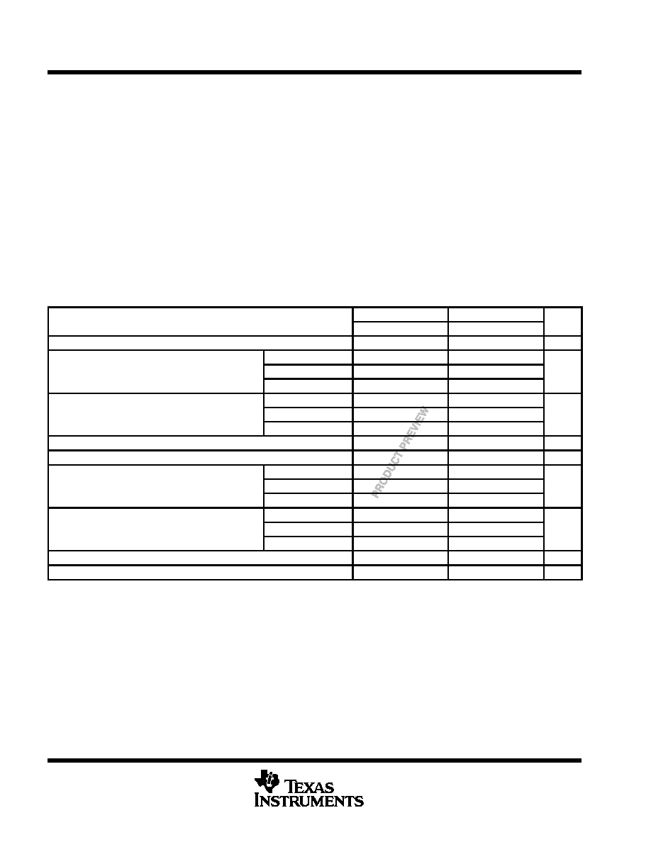
description
The 'AC16646 are 16-bit bus transceivers that
consist of D-type flip-flops and control circuitry,
with 3-state outputs arranged for multiplexed
transmission of data directly from the data bus or
from the internal storage registers. The devices
can be used as two 8-bit transceivers or one 16-bit
transceiver. Data on the A or B bus is clocked into
the registers on the low-to-high transition of the
appropriate clock (CLKAB or CLKBA) input.
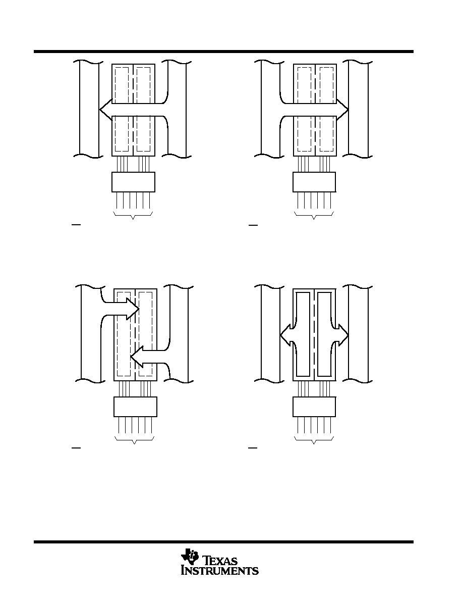
Figure
1 illustrates the four fundamental
bus-management functions that can be
performed with the bus transceivers and
registers.
Output-enable (OE) and direction-control (DIR) inputs are provided to control the transceiver functions. In the
transceiver mode, data present at the high-impedance port may be stored in either register or in both. The select
controls (SAB and SBA) can multiplex stored and real-time (transparent mode) data. The circuitry used for
select control eliminates the typical decoding glitch that occurs in a multiplexer during the transition between
stored and real-time data. DIR determines which bus receives data when OE is active (low). In the isolation
mode (OE high), A data may be stored in one register and/or B data may be stored in the other register.
When an output function is disabled, the input function is still enabled and may be used to store and transmit
data. Only one of the two buses, A or B, may be driven at a time.
The 74AC16646 is packaged in the TI shrink small-outline package, which provides twice the functionality of
standard small-outline packages in the same printed-circuit-board area.
The 54AC16646 is characterized for operation over the full military temperature range of ≠55
∞
C to 125
∞
C. The
74AC16646 is characterized for operation from ≠40
∞
C to 85
∞
C.
Copyright
©
1996, Texas Instruments Incorporated
UNLESS OTHERWISE NOTED this document contains PRODUCTION
DATA information current as of publication date. Products conform to
specifications per the terms of Texas Instruments standard warranty.
Production processing does not necessarily include testing of all
parameters.
Please be aware that an important notice concerning availability, standard warranty, and use in critical applications of
Texas Instruments semiconductor products and disclaimers thereto appears at the end of this data sheet.
EPIC and Widebus are trademarks of Texas Instruments Incorporated.
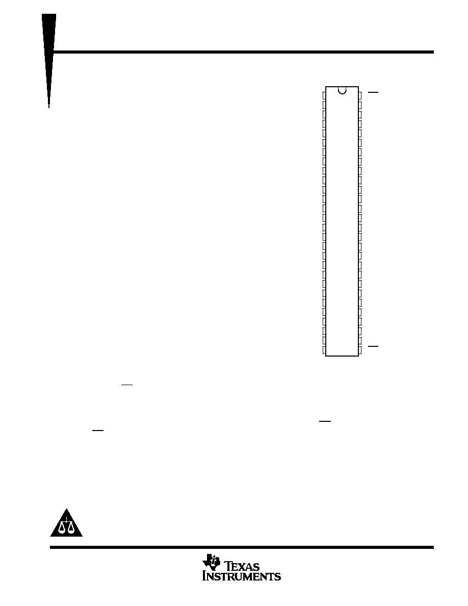
54AC16646 . . . WD PACKAGE
74AC16646 . . . DL PACKAGE
(TOP VIEW)
1
2
3
4
5
6
7
8
9
10
11
12
13
14
15
16
17
18
19
20
21
22
23
24
25
26
27
28
56
55
54
53
52
51
50
49
48
47
46
45
44
43
42
41
40
39
38
37
36
35
34
33
32
31
30
29
1DIR
1CLKAB
1SAB
GND
1A1
1A2
V
CC
1A3
1A4
1A5
GND
1A6
1A7
1A8
2A1
2A2
2A3
GND
2A4
2A5
2A6
V
CC
2A7
2A8
GND
2SAB
2CLKAB
2DIR
1OE
1CLKBA
1SBA
GND
1B1
1B2
V
CC
1B3
1B4
1B5
GND
1B6
1B7
1B8
2B1
2B2
2B3
GND
2B4
2B5
2B6
V
CC
2B7
2B8
GND
2SBA
2CLKBA
2OE
54AC16646, 74AC16646
16-BIT BUS TRANSCEIVERS AND REGISTERS
WITH 3-STATE OUTPUTS
SCAS241A ≠ MARCH 1990 ≠ REVISED APRIL 1996
2
POST OFFICE BOX 655303
∑
DALLAS, TEXAS 75265
L
DIR
L
CLKAB
X
CLKBA
X
SAB
X
SBA
L
REAL-TIME TRANSFER
BUS B TO BUS A
L
DIR
H
CLKAB
X
CLKBA
X
SAB
L
SBA
X
REAL-TIME TRANSFER
BUS A TO BUS B
X
DIR
X
CLKAB CLKBA
X
SAB
X
SBA
X
STORAGE FROM
A, B, OR A AND B
L
DIR
L
CLKAB
X
CLKBA
H or L
SAB
X
SBA
H
TRANSFER STORED DATA
TO A AND/OR B
X
H
X
X
X
X
X
X
X
L
H
H or L
X
H
X
BUS B
BUS A
BUS B
BUS A
BUS B
BUS A
BUS B
BUS A
OE
OE
OE
OE
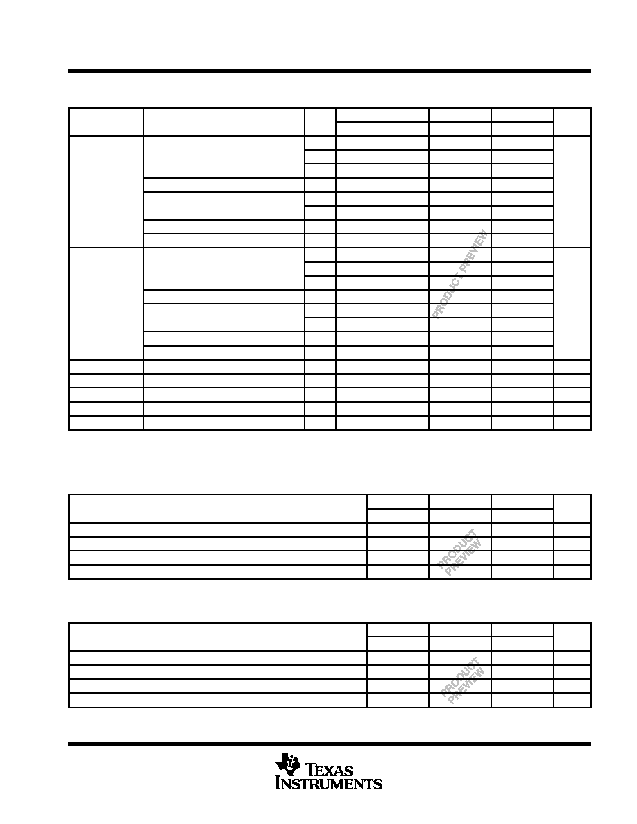
Figure 1. Bus-Management Functions

54AC16646, 74AC16646
16-BIT BUS TRANSCEIVERS AND REGISTERS
WITH 3-STATE OUTPUTS
SCAS241A ≠ MARCH 1990 ≠ REVISED APRIL 1996
3
POST OFFICE BOX 655303
∑
DALLAS, TEXAS 75265
FUNCTION TABLE
INPUTS
DATA I/O
OPERATION OR FUNCTION
OE
DIR
CLKAB
CLKBA
SAB
SBA
A1≠A8
B1≠B8
OPERATION OR FUNCTION
X
X
X
X
X
Input
Unspecified
Store A, B unspecified
{
X
X
X
X
X
Unspecified
Input
Store B, A unspecified
{
H
X
X
X
Input
Input
Store A and B data
H
X
H or L
H or L
X
X
Input
Input
Isolation, hold storage
L
L
X
X
X
L
Output
Input
Real-time B data to A bus
L
L
X
H or L
X
H
Output
Input
Stored B data to A bus
L
H
X
X
L
X
Input
Output
Real-time A data to B Bus
L
H
H or L
X
H
X
Input
Output
Stored A data to bus
The data-output functions may be enabled or disabled by various signals at OE or DIR. Data-input functions are always enabled, i.e., data at
the bus terminals is stored on every low-to-high transition of the clock inputs.
54AC16646, 74AC16646
16-BIT BUS TRANSCEIVERS AND REGISTERS
WITH 3-STATE OUTPUTS
SCAS241A ≠ MARCH 1990 ≠ REVISED APRIL 1996
4
POST OFFICE BOX 655303
∑
DALLAS, TEXAS 75265
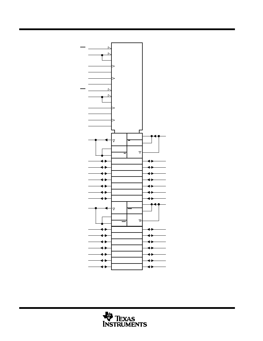
logic symbol
1A2
6
1A3
8
1A4
9
1A5
10
1A6
12
1A7
13
1A8
14
2A2
16
2A3
17
2A4
19
2A5
20
2A6
21
2A7
23
2A8
24
5
1A1
1B6
45
1B7
44
1B8
43
1B2
51
1B3
49
1B4
48
1B5
47
1B1
52
4D
1
2
G12
31
2SBA
30
2CLKBA
10 EN8 [BA]
28
2DIR
G10
29
2B6
36
2B7
34
2B8
33
2B2
41
2B3
40
2B4
38
2B5
37
2OE
10 EN9 [AB]
1
1
5
5
1
1
7
7
15
2A1
8
9
1
1
12
12
1
1
14
14
13D
2B1
42
11D
C11
G14
26
2SAB
27
2CLKAB
C13
G5
54
1SBA
55
1CLKBA
3 EN1 [BA]
1
1DIR
G3
56
1OE
3 EN2 [AB]
C4
G7
3
1SAB
2
1CLKAB
C6
6D
This symbol is in accordance with ANSI/IEEE Std 91-1984 and IEC Publication 617-12.
54AC16646, 74AC16646
16-BIT BUS TRANSCEIVERS AND REGISTERS
WITH 3-STATE OUTPUTS
SCAS241A ≠ MARCH 1990 ≠ REVISED APRIL 1996
5
POST OFFICE BOX 655303
∑
DALLAS, TEXAS 75265
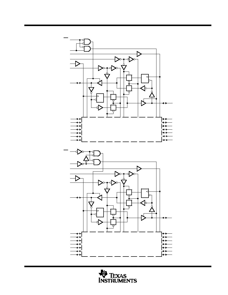
logic diagram (positive logic)
B8
B7
B6
B5
B4
B3
B2
33
34
36
37
38
40
41
2A8
2A7
2A6
2A5
2A4
2A3
2A2
24
23
21
20
19
17
16
2A1
2SAB
2CLKAB
2SBA
2CLKBA
2DIR
2OE
15
26
27
31
30
28
29
TG
TG
TG
TG
C1
1D
1D
C1
42
B1
Seven Channels Identical
to Channel One Above
Seven Channels Identical
to Channel One Above
B8
B7
B6
B5
B4
B3
B2
B1
47
48
49
51
52
1A8
1A7
1A6
1A5
1A4
1A3
1A2
14
13
12
10
9
8
6
1A1
5
1SAB
1CLKAB
1SBA
1CLKBA
1DIR
1OE
3
2
54
55
1
56
C1
1D
1D
C1
TG
TG
TG
TG
45
44
43
54AC16646, 74AC16646
16-BIT BUS TRANSCEIVERS AND REGISTERS
WITH 3-STATE OUTPUTS
SCAS241A ≠ MARCH 1990 ≠ REVISED APRIL 1996
6
POST OFFICE BOX 655303
∑
DALLAS, TEXAS 75265
absolute maximum ratings over operating free-air temperature range (unless otherwise noted)
Supply voltage range, V
CC
≠0.5 V to 7 V
. . . . . . . . . . . . . . . . . . . . . . . . . . . . . . . . . . . . . . . . . . . . . . . . . . . . . . . . . .
Input voltage range, V
I
(see Note 1)
≠0.5 V to V
CC
+ 0.5 V
. . . . . . . . . . . . . . . . . . . . . . . . . . . . . . . . . . . . . . . . . . .
Output voltage range, V
O
(see Note 1)
≠0.5 V to V
CC
+ 0.5 V
. . . . . . . . . . . . . . . . . . . . . . . . . . . . . . . . . . . . . . . .
Input clamp current, I
IK
(V
I
< 0 or V
I
> V
CC
)
±
20 mA
. . . . . . . . . . . . . . . . . . . . . . . . . . . . . . . . . . . . . . . . . . . . . . . .
Output clamp current, I
OK
(V
O
< 0 or V
O
> V
CC
)
±
50 mA
. . . . . . . . . . . . . . . . . . . . . . . . . . . . . . . . . . . . . . . . . . . .
Continuous output current, I
O
(V
O
= 0 to V
CC
±
50 mA
. . . . . . . . . . . . . . . . . . . . . . . . . . . . . . . . . . . . . . . . . . . . . . .
Continuous current through V
CC
or GND
±
400 mA
. . . . . . . . . . . . . . . . . . . . . . . . . . . . . . . . . . . . . . . . . . . . . . . . . .
Maximum power dissipation at T
A
= 55
∞
C (in still air) (see Note 2): DL package
1.4 W
. . . . . . . . . . . . . . . . . . .
Storage temperature range, T
stg
≠65
∞
C to 150
∞
C
. . . . . . . . . . . . . . . . . . . . . . . . . . . . . . . . . . . . . . . . . . . . . . . . . . .
Stresses beyond those listed under "absolute maximum ratings" may cause permanent damage to the device. These are stress ratings only, and
functional operation of the device at these or any other conditions beyond those indicated under "recommended operating conditions" is not
implied. Exposure to absolute-maximum-rated conditions for extended periods may affect device reliability.
NOTES:
1. The input and output voltage ratings may be exceeded if the input and output current ratings are observed.
2. The maximum package power dissipation is calculated using a junction temperature of 150
_
C and a board trace length of 750 mils.
recommended operating conditions
54AC16646
74AC16646
UNIT
MIN
NOM
MAX
MIN
NOM
MAX
UNIT
VCC
Supply voltage (see Note 3)
3
5
5.5
3
5
5.5
V
VCC = 3 V
2.1
2.1
VIH
High-level input voltage
VCC = 4.5 V
3.15
3.15
V
VCC = 5.5 V
3.85
3.85
VCC = 3 V
0.9
0.9
VIL
Low-level input voltage
VCC = 4.5 V
1.35
1.35
V
VCC = 5.5 V
1.65
1.65
VI
Input voltage
0
VCC
0
VCC
V
VO
Output voltage
0
VCC
0
VCC
V
VCC = 3 V
≠4
≠4
IOH
High-level output current
VCC = 4.5 V
≠24
≠24
mA
VCC = 5.5 V
≠24
≠24
VCC = 3 V
12
12
IOL
Low-level output current
VCC = 4.5 V
24
24
mA
VCC = 5.5 V
24
24
t/
v
Input transition rise or fall rate
0
10
0
10
ns/V
TA
Operating free-air temperature
≠55
125
≠40
85
∞
C
NOTE 3: All VCC and GND pins must be connected to the proper voltage power supply.
PRODUCT PREVIEW information concerns products in the formative or
design phase of development. Characteristic data and other specifications
are design goals. Texas Instruments reserves the right to change or
discontinue these products without notice.
54AC16646, 74AC16646
16-BIT BUS TRANSCEIVERS AND REGISTERS
WITH 3-STATE OUTPUTS
SCAS241A ≠ MARCH 1990 ≠ REVISED APRIL 1996
7
POST OFFICE BOX 655303
∑
DALLAS, TEXAS 75265
electrical characteristics over recommended operating free-air temperature range (unless
otherwise noted)
PARAMETER
TEST CONDITIONS
VCC
TA = 25
∞
C
54AC16646
74AC16646
UNIT
PARAMETER
TEST CONDITIONS
VCC
MIN
TYP
MAX
MIN
MAX
MIN
MAX
UNIT
3 V
2.9
2.9
2.9
IOH = ≠50
µ
A
4.5 V
4.4
4.4
4.4
5.5 V
5.4
5.4
5.4
VOH
IOH = ≠4 mA
3 V
2.58
2.4
2.48
V
VOH
4.5 V
3.94
3.7
3.8
V
5.5 V
4.94
4.7
4.8
IOH = ≠50 mA
5.5 V
3.85
IOH = ≠75 mA
5.5 V
3.85
3 V
0.1
0.1
0.1
IOL = 50
µ
A
4.5 V
0.1
0.1
0.1
5.5 V
0.1
0.1
0.1
VOL
IOL = 12 mA
3 V
0.36
0.5
0.44
V
VOL
4.5 V
0.36
0.5
0.44
V
5.5 V
0.36
0.5
0.44
IOL = 50 mA
5.5 V
1.65
IOL = 75 mA
5.5 V
1.65
II
VI = VCC or GND
5.5 V
±
0.1
±
1
±
1
µ
A
IOZ
VI = VCC or GND
5.5 V
±
0.5
±
10
±
5
µ
A
ICC
VI = VCC or GND,
IO = 0
5.5 V
8
160
80
µ
A
Ci
VI = VCC or GND
5 V
4.5
pF
Co
VI = VCC or GND
5 V
16
pF
Not more than one output should be tested at a time, and the duration of the test should not exceed 10 ms.
For I/O ports, the parameter IOZ includes the input leakage current.
timing requirements over recommended operating free-air temperature range,
V
CC
= 3.3 V
±
0.3 V (unless otherwise noted) (see Figure 2)
TA = 25
∞
C
54AC16646
74AC16646
UNIT
MIN
MAX
MIN
MAX
MIN
MAX
UNIT
fclock
Clock frequency
0
65
0
65
0
65
MHz
tw
Pulse duration, CLKAB or CLKBA high or low
7
7
7
ns
tsu
Setup time, A before CLKAB
or B before CLKBA
6.5
6.5
6.5
ns
th
Hold time, A after CLKAB
or B after CLKBA
1
1
1
ns
timing requirements over recommended operating free-air temperature range,
V
CC
= 5 V
±
0.5 V (unless otherwise noted) (see Figure 2)
TA = 25
∞
C
54AC16646
74AC16646
UNIT
MIN
MAX
MIN
MAX
MIN
MAX
UNIT
fclock
Clock frequency
0
75
0
75
0
75
MHz
tw
Pulse duration, CLKAB or CLKBA high or low
6.5
6.5
6.5
ns
tsu
Setup time, A before CLKAB
or B before CLKBA
5
5
5
ns
th
Hold time, A after CLKAB
or B after CLKBA
1
1
1
ns
PRODUCT PREVIEW information concerns products in the formative or
design phase of development. Characteristic data and other specifications
are design goals. Texas Instruments reserves the right to change or
discontinue these products without notice.
PRODUCT PREVIEW information concerns products in the formative or
design phase of development. Characteristic data and other
specifications are design goals. Texas Instruments reserves the right to
change or discontinue these products without notice.
54AC16646, 74AC16646
16-BIT BUS TRANSCEIVERS AND REGISTERS
WITH 3-STATE OUTPUTS
SCAS241A ≠ MARCH 1990 ≠ REVISED APRIL 1996
8
POST OFFICE BOX 655303
∑
DALLAS, TEXAS 75265
switching characteristics over recommended operating free-air temperature range,
V
CC
= 3.3 V
±
0.3 V (unless otherwise noted) (see Figure 2)
PARAMETER
FROM
TO
TA = 25
∞
C
54AC16646
74AC16646
UNIT
PARAMETER
(INPUT)
(OUTPUT)
MIN
TYP
MAX
MIN
MAX
MIN
MAX
UNIT
fmax
65
65
65
MHz
tPLH
A or B
B or A
3.4
9.3
13.2
3.4
15.7
3.4
14.8
ns
tPHL
A or B
B or A
3.6
10
13.4
3.6
15.1
3.6
4.5
ns
tPZH
OE
A or B
3.8
10.5
3.8
17.6
3.8
16.4
ns
tPZL
OE
A or B
4.8
13.9
4.8
22.1
4.8
20.9
ns
tPHZ
OE
A or B
4.4
7.6
4.4
11
4.4
10.7
ns
tPLZ
OE
A or B
4
7
4
10.4
4
10.1
ns
tPLH
CLKBA or CLKAB
A or B
4.7
12.1
4.7
19.9
4.7
18.7
ns
tPHL
CLKBA or CLKAB
A or B
4.8
12.2
4.8
18.8
4.8
18
ns
tPLH
SAB or SBA
A or B
4.7
12
4.7
19.9
4.7
18.5
ns
tPHL
(with A or B high)
A or B
4.5
11.4
4.5
17.2
4.5
16.4
ns
tPLH
SBA or SAB
A or B
4
10.5
4
17.3
4
16.3
ns
tPHL
(with A or B low)
A or B
5.2
13.3
5.2
20.3
5.2
19.3
ns
tPZH
DIR
A or B
3.6
10.3
3.6
17.9
3.6
16.8
ns
tPZL
DIR
A or B
4.7
13.5
4.7
22.1
4.7
20.8
ns
tPHZ
DIR
A or B
4.6
7.8
4.6
11.6
4.6
11.2
ns
tPLZ
DIR
A or B
3.9
7
3.9
11
3.9
10.6
ns
These parameters are measured with the internal output state of the storage register opposite that of the bus input.
switching characteristics over recommended operating free-air temperature range,
V
CC
= 5 V
±
0.5 V (unless otherwise noted) (see Figure 2)
PARAMETER
FROM
TO
TA = 25
∞
C
54AC16646
74AC16646
UNIT
PARAMETER
(INPUT)
(OUTPUT)
MIN
TYP
MAX
MIN
MAX
MIN
MAX
UNIT
fmax
75
75
75
MHz
tPLH
A or B
B or A
2.9
5.5
8.5
2.9
10.1
2.9
9.5
ns
tPHL
A or B
B or A
2.9
5.7
8.9
2.9
10.1
2.9
9.7
ns
tPZH
OE
A or B
3.1
6.1
9.4
3.1
11.1
3.1
10.5
ns
tPZL
OE
A or B
4.1
7.3
11
4.1
12.9
4.1
12.2
ns
tPHZ
OE
A or B
4
6.1
8.4
4
9.1
4
8.9
ns
tPLZ
OE
A or B
3.8
5.7
8
3.8
8.9
3.8
8.6
ns
tPLH
CLKBA or CLKAB
A or B
3.9
7
10.8
3.9
12.8
3.9
12.1
ns
tPHL
CLKBA or CLKAB
A or B
3.9
7.1
10.8
3.9
12.5
3.9
11.9
ns
tPLH
SAB or SBA
A or B
4
7.4
11.1
4
13.4
4
12.5
ns
tPHL
(with A or B high)
A or B
3.6
6.7
10.2
3.6
11.8
3.6
11.2
ns
tPLH
SBA or SAB
A or B
3.3
6.1
9.5
3.3
11.2
3.3
10.6
ns
tPHL
(with A or B low)
A or B
4.3
8
11.7
4.3
13.9
4.3
13.1
ns
tPZH
DIR
A or B
3
5.9
9.6
3
11.6
3
10.9
ns
tPZL
DIR
A or B
3.6
7
11.1
3.6
12.9
3.6
12.2
ns
tPHZ
DIR
A or B
4
6.2
8.8
4
9.6
3
9.4
ns
tPLZ
DIR
A or B
3.7
5.7
8.2
3.7
9
3.7
8.8
ns
These parameters are measured with the internal output state of the storage register opposite that of the bus input.

54AC16646, 74AC16646
16-BIT BUS TRANSCEIVERS AND REGISTERS
WITH 3-STATE OUTPUTS
SCAS241A ≠ MARCH 1990 ≠ REVISED APRIL 1996
9
POST OFFICE BOX 655303
∑
DALLAS, TEXAS 75265
operating characteristics, V
CC
= 5 V, T
A
= 25
∞
C
PARAMETER
TEST CONDITIONS
TYP
UNIT
C d
Power dissipation capacitance
Outputs enabled
CL = 50 pF
f = 1 MHz
62
pF
Cpd
Power dissipation capacitance
Outputs disabled
CL = 50 pF,
f = 1 MHz
14
pF
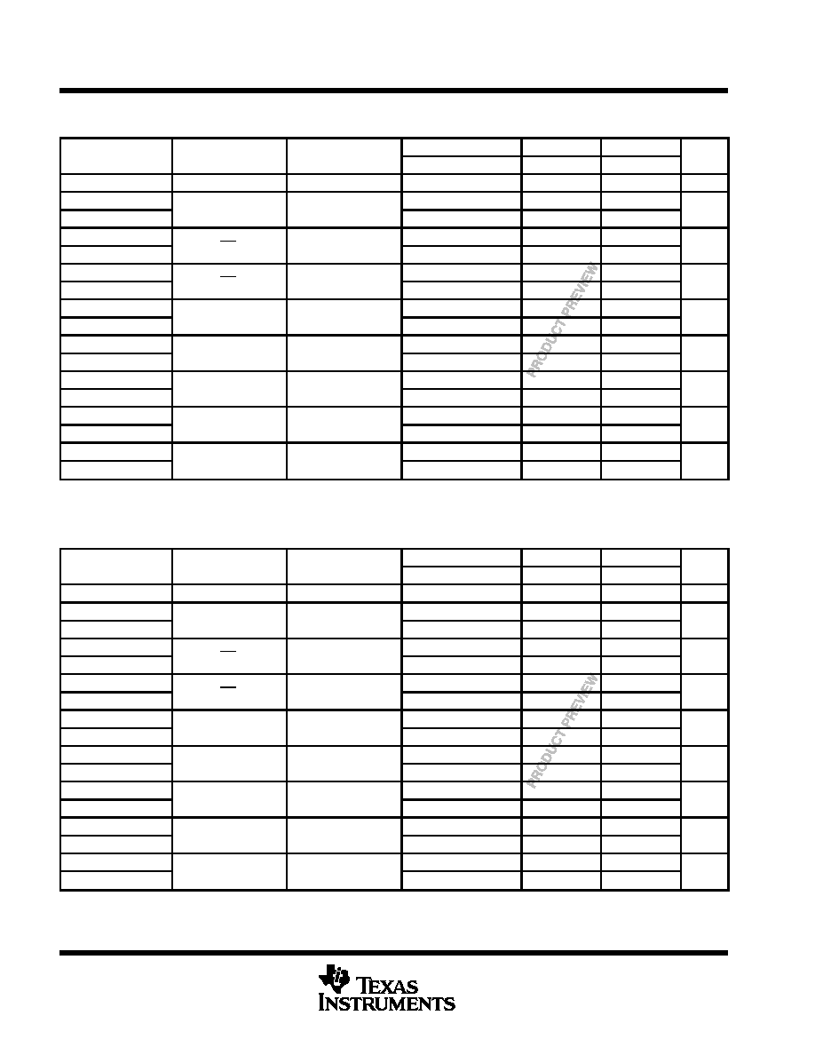
PARAMETER MEASUREMENT INFORMATION
50% VCC
50%
50%
50%
VCC
VCC
0 V
0 V
th
tsu
VOLTAGE WAVEFORMS
Data Input
tPLH
tPHL
tPHL
tPLH
VOH
VOH
VOL
VOL
50%
50%
VCC
0 V
50% VCC
50% VCC
Input
Out-of-Phase
Output
In-Phase
Output
Timing Input
50% VCC
VOLTAGE WAVEFORMS
From Output
Under Test
CL = 50 pF
(see Note A)
LOAD CIRCUIT
S1
2
◊
VCC
500
500
Output
Control
(low-level
enabling)
Output
Waveform 1
S1 at 2
◊
VCC
(see Note B)
Output
Waveform 2
S1 at GND
(see Note B)
VOL
VOH
tPZL
tPZH
tPLZ
tPHZ
50%
50%
[
VCC
0 V
50% VCC
20% VCC
50% VCC
80% VCC
[
0 V
VCC
GND
Open
VOLTAGE WAVEFORMS
tPLH/tPHL
tPLZ/tPZL
tPHZ/tPZH
Open
2
◊
VCC
GND
TEST
S1
VCC
0 V
50%
50%
tw
VOLTAGE WAVEFORMS
Input
NOTES: A. CL includes probe and jig capacitance.
B. Waveform 1 is for an output with internal conditions such that the output is low except when disabled by the output control.
Waveform 2 is for an output with internal conditions such that the output is high except when disabled by the output control.
C. All input pulses are supplied by generators having the following characteristics: PRR
1 MHz, ZO = 50
, tr = 3 ns, tf = 3 ns.
D. The outputs are measured one at a time with one input transition per measurement.
Figure 2. Load Circuit and Voltage Waveforms

IMPORTANT NOTICE
Texas Instruments and its subsidiaries (TI) reserve the right to make changes to their products or to discontinue
any product or service without notice, and advise customers to obtain the latest version of relevant information
to verify, before placing orders, that information being relied on is current and complete. All products are sold
subject to the terms and conditions of sale supplied at the time of order acknowledgement, including those
pertaining to warranty, patent infringement, and limitation of liability.
TI warrants performance of its semiconductor products to the specifications applicable at the time of sale in
accordance with TI's standard warranty. Testing and other quality control techniques are utilized to the extent
TI deems necessary to support this warranty. Specific testing of all parameters of each device is not necessarily
performed, except those mandated by government requirements.
CERTAIN APPLICATIONS USING SEMICONDUCTOR PRODUCTS MAY INVOLVE POTENTIAL RISKS OF
DEATH, PERSONAL INJURY, OR SEVERE PROPERTY OR ENVIRONMENTAL DAMAGE ("CRITICAL
APPLICATIONS"). TI SEMICONDUCTOR PRODUCTS ARE NOT DESIGNED, AUTHORIZED, OR
WARRANTED TO BE SUITABLE FOR USE IN LIFE-SUPPORT DEVICES OR SYSTEMS OR OTHER
CRITICAL APPLICATIONS. INCLUSION OF TI PRODUCTS IN SUCH APPLICATIONS IS UNDERSTOOD TO
BE FULLY AT THE CUSTOMER'S RISK.
In order to minimize risks associated with the customer's applications, adequate design and operating
safeguards must be provided by the customer to minimize inherent or procedural hazards.
TI assumes no liability for applications assistance or customer product design. TI does not warrant or represent
that any license, either express or implied, is granted under any patent right, copyright, mask work right, or other
intellectual property right of TI covering or relating to any combination, machine, or process in which such
semiconductor products or services might be or are used. TI's publication of information regarding any third
party's products or services does not constitute TI's approval, warranty or endorsement thereof.
Copyright
©
1998, Texas Instruments Incorporated