 | –≠–ª–µ–∫—Ç—Ä–æ–Ω–Ω—ã–π –∫–æ–º–ø–æ–Ω–µ–Ω—Ç: 74AC175 | –°–∫–∞—á–∞—Ç—å:  PDF PDF  ZIP ZIP |
1
Data sheet acquired from Harris Semiconductor
SCHS242
Features
∑ Buffered Inputs
∑ Typical Propagation Delay
- 6.4ns at V
CC
= 5V, T
A
= 25
o
C, C
L
= 50pF
∑ Exceeds 2kV ESD Protection MIL-STD-883, Method
3015
∑ SCR-Latchup-Resistant CMOS Process and Circuit
Design
∑ Speed of Bipolar FASTTM/AS/S with Significantly
Reduced Power Consumption
∑ Balanced Propagation Delays
∑ AC Types Feature 1.5V to 5.5V Operation and
Balanced Noise Immunity at 30% of the Supply
∑
±
24mA Output Drive Current
- Fanout to 15 FASTTM ICs
- Drives 50
Transmission Lines
Description
The CD74AC175 and CD74ACT175 are quad D flip-flops
with reset that utilize the Harris Advanced CMOS Logic tech-
nology. Information at the D input is transferred to the Q and
Q outputs on the positive-going edge of the clock pulse. All
four flip-flops are controlled by a common clock (CP) and a
common reset (MR). Resetting is accomplished by a LOW
logic level independent of the clock.
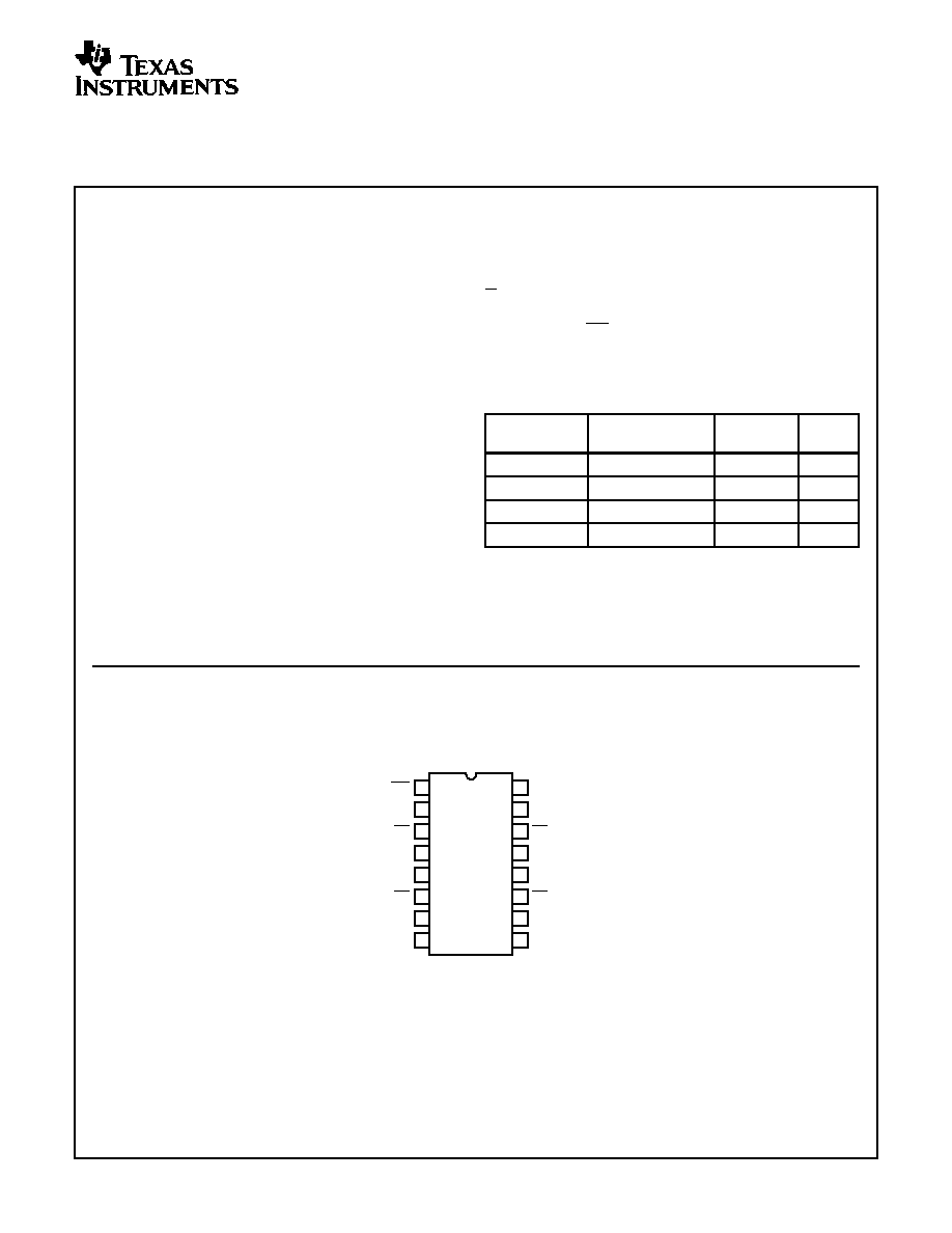
Pinout
CD74AC175, CD74ACT175
(PDIP, SOIC)
TOP VIEW
Ordering Information
PART
NUMBER
TEMP.
RANGE (
o
C)
PACKAGE
PKG.
NO.
CD74AC175E
-55 to 125
16 Ld PDIP
E16.3
CD74ACT175E
-55 to 125
16 Ld PDIP
E16.3
CD74AC175M
-55 to 125
16 Ld SOIC
M16.15
CD74ACT175M
-55 to 125
16 Ld SOIC
M16.15
NOTES:
13. When ordering, use the entire part number. Add the suffix 96 to
obtain the variant in the tape and reel.
14. Wafer and die for this part number is available which meets all elec-
trical specifications. Please contact your local sales office or Harris
customer service for ordering information.
14
15
16
9
13
12
11
10
1
2
3
4
5
7
6
8
MR
Q0
Q0
D0
D1
Q1
GND
Q1
V
CC
Q3
D3
D2
Q2
Q2
CP
Q3
September 1998
CAUTION: These devices are sensitive to electrostatic discharge. Users should follow proper IC Handling Procedures.
FASTTM is a Trademark of Fairchild Semiconductor.
Copyright
©
Harris Corporation 1998
CD74AC175,
CD74ACT175
Quad D Flip-Flop with Reset
File Number
1964.1
[ /Title
(CD74
AC175
,
CD74
ACT17
5
)
/Sub-
ject
(Quad
D Flip-
Flop
with
Reset)
/Autho
r ()
/Key-
words
(Har-
ris
Semi-
con-
ductor,
Advan
ced
CMOS
, Harris
Semi-
con-
ductor,
Advan
ced
TTL)
/Cre-
ator ()
/DOCI
NFO
2
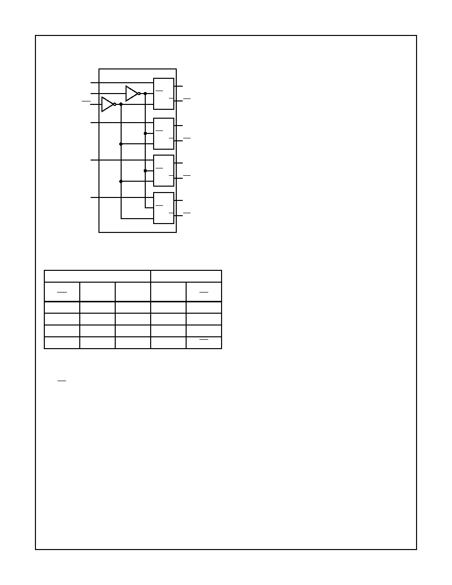
Functional Diagram
TRUTH TABLE (EACH FLIP-FLOP)
INPUTS
OUTPUTS
RESET
(MR)
CLOCK
CP
DATA
Dn
Qn
Qn
L
X
X
L
H
H
H
H
L
H
L
L
H
H
L
X
Q0
Q0
H
= High Level (Steady State)
L
= Low Level (Steady State)
X
= Irrelevant
= Transition from Low to High level
Q0, Q0 = Level before the Indicated Steady-State Input conditions
were established.
CP
D
R
2
Q0
9
4
D0
CP
Q
Q
3
Q0
MR
1
CP
D
R
7
Q1
5
D1
Q
Q
6
Q1
CP
D
R
10
Q2
12
D2
Q
Q
11
Q2
CP
D
R
15
Q3
13
D3
Q
Q
14
Q3
GND = 8
V
CC
= 16
CD74AC175, CD74ACT175

3
Absolute Maximum Ratings
Thermal Information
DC Supply Voltage, V
CC
. . . . . . . . . . . . . . . . . . . . . . . . -0.5V to 6V
DC Input Diode Current, I
IK
For V
I
< -0.5V or V
I
> V
CC
+ 0.5V
. . . . . . . . . . . . . . . . . . . . . .±
20mA
DC Output Diode Current, I
OK
For V
O
< -0.5V or V
O
> V
CC
+ 0.5V
. . . . . . . . . . . . . . . . . . . .±
50mA
DC Output Source or Sink Current per Output Pin, I
O
For V
O
> -0.5V or V
O
< V
CC
+ 0.5V
. . . . . . . . . . . . . . . . . . . .±
50mA
DC V
CC
or Ground Current, I
CC or
I
GND
(Note 3)
. . . . . . . . .±
100mA
Operating Conditions
Temperature Range, T
A
. . . . . . . . . . . . . . . . . . . . . . -55
o
C to 125
o
C
Supply Voltage Range, V
CC
(Note 4)
AC Types. . . . . . . . . . . . . . . . . . . . . . . . . . . . . . . . . . .1.5V to 5.5V
ACT Types . . . . . . . . . . . . . . . . . . . . . . . . . . . . . . . . .4.5V to 5.5V
DC Input or Output Voltage, V
I
, V
O
. . . . . . . . . . . . . . . . . 0V to V
CC
Input Rise and Fall Slew Rate, dt/dv
AC Types, 1.5V to 3V . . . . . . . . . . . . . . . . . . . . . . . . . 50ns (Max)
AC Types, 3.6V to 5.5V . . . . . . . . . . . . . . . . . . . . . . . . 20ns (Max)
ACT Types, 4.5V to 5.5V. . . . . . . . . . . . . . . . . . . . . . . 10ns (Max)
Thermal Resistance (Typical, Note 5)
JA
(
o
C/W)
PDIP Package . . . . . . . . . . . . . . . . . . . . . . . . . . . . .
90
SOIC Package . . . . . . . . . . . . . . . . . . . . . . . . . . . . .
160
Maximum Junction Temperature (Plastic Package) . . . . . . . . . . 150
o
C
Maximum Storage Temperature Range . . . . . . . . . .-65
o
C to 150
o
C
Maximum Lead Temperature (Soldering 10s) . . . . . . . . . . . . . 300
o
C
(SOIC - Lead Tips Only)
CAUTION: Stresses above those listed in "Absolute Maximum Ratings" may cause permanent damage to the device. This is a stress only rating and operation
of the device at these or any other conditions above those indicated in the operational sections of this specification is not implied.
NOTES:
15. For up to 4 outputs per device, add
±
25mA for each additional output.
16. Unless otherwise specified, all voltages are referenced to ground.
17.
JA
is measured with the component mounted on an evaluation PC board in free air.
DC Electrical Specifications
PARAMETER
SYMBOL
TEST
CONDITIONS
V
CC
(V)
25
o
C
-40
o
C TO
85
o
C
-55
o
C TO
125
o
C
UNITS
V
I
(V)
I
O
(mA)
MIN
MAX
MIN
MAX
MIN
MAX
AC TYPES
High Level Input Voltage
V
IH
-
-
1.5
1.2
-
1.2
-
1.2
-
V
3
2.1
-
2.1
-
2.1
-
V
5.5
3.85
-
3.85
-
3.85
-
V
Low Level Input Voltage
V
IL
-
-
1.5
-
0.3
-
0.3
-
0.3
V
3
-
0.9
-
0.9
-
0.9
V
5.5
-
1.65
-
1.65
-
1.65
V
High Level Output Voltage
V
OH
V
IH
or V
IL
-0.05
1.5
1.4
-
1.4
-
1.4
-
V
-0.05
3
2.9
-
2.9
-
2.9
-
V
-0.05
4.5
4.4
-
4.4
-
4.4
-
V
-4
3
2.58
-
2.48
-
2.4
-
V
-24
4.5
3.94
-
3.8
-
3.7
-
V
-75
(Note 6, 7)
5.5
-
-
3.85
-
-
-
V
-50
(Note 6, 7)
5.5
-
-
-
-
3.85
-
V
CD74AC175, CD74ACT175

4
Low Level Output Voltage
V
OL
V
IH
or V
IL
0.05
1.5
-
0.1
-
0.1
-
0.1
V
0.05
3
-
0.1
-
0.1
-
0.1
V
0.05
4.5
-
0.1
-
0.1
-
0.1
V
12
3
-
0.36
-
0.44
-
0.5
V
24
4.5
-
0.36
-
0.44
-
0.5
V
75
(Note 6, 7)
5.5
-
-
-
1.65
-
-
V
50
(Note 6, 7)
5.5
-
-
-
-
-
1.65
V
Input Leakage Current
I
I
V
CC
or
GND
-
5.5
-
±
0.1
-
±
1
-
±
1
µ
A
Quiescent Supply Current
MSI
I
CC
V
CC
or
GND
0
5.5
-
8
-
80
-
160
µ
A
ACT TYPES
High Level Input Voltage
V
IH
-
-
4.5 to
5.5
2
-
2
-
2
-
V
Low Level Input Voltage
V
IL
-
-
4.5 to
5.5
-
0.8
-
0.8
-
0.8
V
High Level Output Voltage
V
OH
V
IH
or V
IL
-0.05
4.5
4.4
-
4.4
-
4.4
-
V
-24
4.5
3.94
-
3.8
-
3.7
-
V
-75
(Note 6, 7)
5.5
-
-
3.85
-
-
-
V
-50
(Note 6, 7)
5.5
-
-
-
-
3.85
-
V
Low Level Output Voltage
V
OL
V
IH
or V
IL
0.05
4.5
-
0.1
-
0.1
-
0.1
V
24
4.5
-
0.36
-
0.44
-
0.5
V
75
(Note 6, 7)
5.5
-
-
-
1.65
-
-
V
50
(Note 6, 7)
5.5
-
-
-
-
-
1.65
V
Input Leakage Current
I
I
V
CC
or
GND
-
5.5
-
±
0.1
-
±
1
-
±
1
µ
A
Quiescent Supply Current
MSI
I
CC
V
CC
or
GND
0
5.5
-
8
-
80
-
160
µ
A
Additional Supply Current per
Input Pin TTL Inputs High
1 Unit Load
I
CC
V
CC
-2.1
-
4.5 to
5.5
-
2.4
-
2.8
-
3
mA
NOTES:
18. Test one output at a time for a 1-second maximum duration. Measurement is made by forcing current and measuring voltage to minimize
power dissipation.
19. Test verifies a minimum 50
transmission-line-drive capability at 85
o
C, 75
at 125
o
C.
ACT Input Load Table
INPUT
UNIT LOAD
Dn
0.58
MR
0.67
CP
0.92
NOTE: Unit load is
I
CC
limit specified in DC Electrical Specifications
Table, e.g., 2.4mA max at 25
o
C.
DC Electrical Specifications
(Continued)
PARAMETER
SYMBOL
TEST
CONDITIONS
V
CC
(V)
25
o
C
-40
o
C TO
85
o
C
-55
o
C TO
125
o
C
UNITS
V
I
(V)
I
O
(mA)
MIN
MAX
MIN
MAX
MIN
MAX
CD74AC175, CD74ACT175

5
Prerequisite For Switching Function
PARAMETER
SYMBOL
V
CC
(V)
-40
o
C TO 85
o
C
-55
o
C TO 125
o
C
UNITS
MIN
MAX
MIN
MAX
AC TYPES
Data to CP Set-Up Time
t
SU
1.5
2
-
2
-
ns
3.3
(Note 8)
2
-
2
-
ns
5
(Note 9)
2
-
2
-
ns
Hold Time
t
H
1.5
2
-
2
-
ns
3.3
2
-
2
-
ns
5
2
-
2
-
ns
Removal Time, MR to CP
t
REM
1.5
1
-
1
-
ns
3.3
1
-
1
-
ns
5
1
-
1
-
ns
MR Pulse Width
t
W
1.5
44
-
50
-
ns
3.3
4.9
-
5.6
-
ns
5
3.5
-
4
-
ns
CP Pulse Width
t
W
1.5
55
-
63
-
ns
3.3
6.1
-
7
-
ns
5
4.4
-
5
-
ns
CP Frequency
f
MAX
1.5
9
-
8
-
MHz
3.3
81
-
71
-
MHz
5
114
-
100
-
MHz
ACT TYPES
Data to CP Set-Up Time
t
SU
5
(Note 9)
2
-
2
-
ns
Hold Time
t
H
5
2
-
2
-
ns
Removal Time, MR to CP
t
REM
5
1
-
1
-
ns
MR Pulse Width
t
W
5
3.5
-
4
-
ns
Clock Pulse Width
t
W
5
4.4
-
5
-
ns
CP Frequency
f
MAX
5
114
-
114
-
MHz
NOTES:
20. 3.3V Min is at 3V.
21. 5V Min is at 4.5V.
Switching Specifications
Input t
r
, t
f
= 3ns, C
L
= 50pF (Worst Case)
PARAMETER
SYMBOL
V
CC
(V)
-40
o
C TO 85
o
C
-55
o
C TO 125
o
C
UNITS
MIN
TYP
MAX
MIN
TYP
MAX
AC TYPES
Propagation Delay, CP to Q, Q
t
PLH
, t
PHL
1.5
-
-
139
-
-
153
ns
3.3
(Note 11)
4.4
-
15.5
4.3
-
17.1
ns
5
(Note 12)
3.2
-
11.1
3.1
-
12.2
ns
CD74AC175, CD74ACT175