74ACT11004
HEX INVERTER
SCAS215B ≠ JANUARY 1988 ≠ REVISED JUNE 1997
1
POST OFFICE BOX 655303
∑
DALLAS, TEXAS 75265
D
Inputs Are TTL-Voltage Compatible
D
Flow-Through Architecture Optimizes PCB
Layout
D
Center-Pin V
CC
and GND Configurations
Minimize High-Speed Switching Noise
D
EPIC
(Enhanced-Performance Implanted
CMOS) 1-
m
m Process
D
500-mA Typical Latch-Up Immunity at
125
∞
C
D
Package Options Include Plastic
Small-Outline (DW), Shrink Small-Outline
(DB), and Thin Shrink Small-Outline (PW)
Packages and Standard Plastic (N) 300-mil
DIPs
description
This device contains six independent inverters. It performs the Boolean function Y = A.
The 74ACT11004 is characterized for operation from ≠40
∞
C to 85
∞
C.
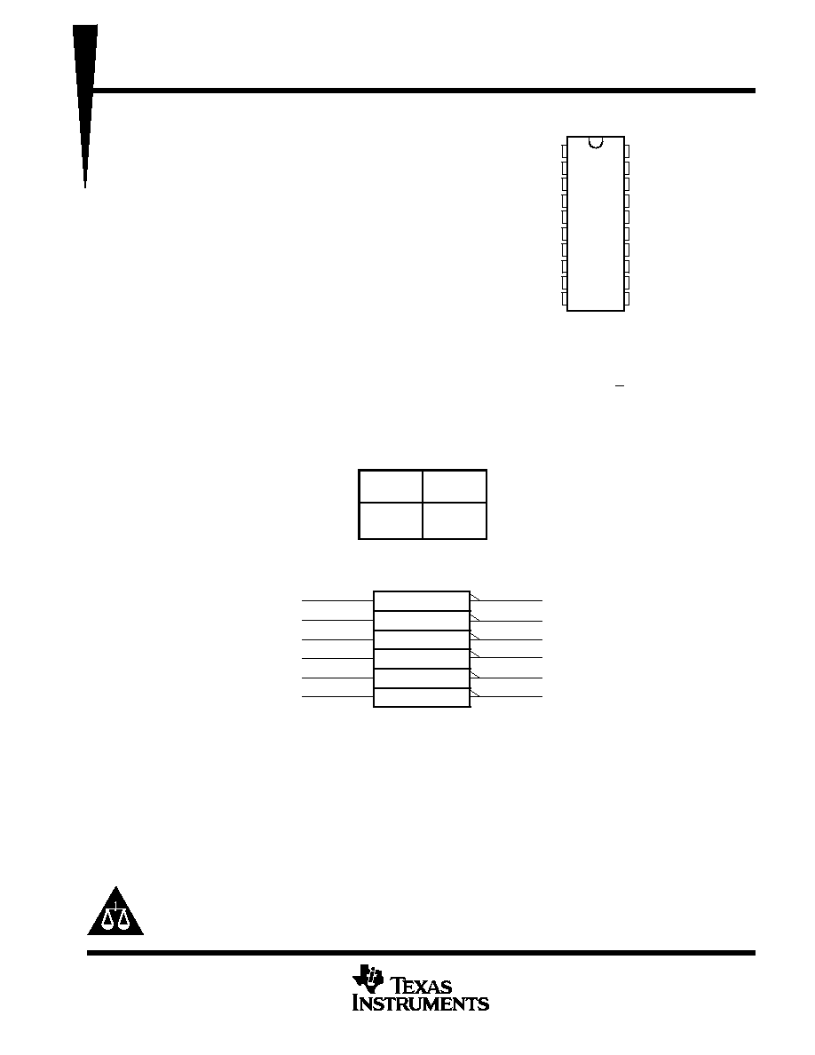
FUNCTION TABLE
(each inverter)
INPUT
A
OUTPUT
Y
H
L
L
H
logic symbol
This symbol is in accordance with ANSI/IEEE Std 91-1984 and IEC Publication 617-12.
20
1A
19
2A
1Y
1
18
3A
13
4A
2Y
2
12
5A
11
6A
3Y
3
4Y
8
5Y
9
6Y
10
1
Copyright
1997, Texas Instruments Incorporated
PRODUCTION DATA information is current as of publication date.
Products conform to specifications per the terms of Texas Instruments
standard warranty. Production processing does not necessarily include
testing of all parameters.
Please be aware that an important notice concerning availability, standard warranty, and use in critical applications of
Texas Instruments semiconductor products and disclaimers thereto appears at the end of this data sheet.
EPIC is a trademark of Texas Instruments Incorporated.
1
2
3
4
5
6
7
8
9
10
20
19
18
17
16
15
14
13
12
11
1Y
2Y
3Y
GND
GND
GND
GND
4Y
5Y
6Y
1A
2A
3A
NC
V
CC
V
CC
NC
4A
5A
6A
DB, DW, N, OR PW PACKAGE
(TOP VIEW)
NC ≠ No internal connection

74ACT11004
HEX INVERTER
SCAS215B ≠ JANUARY 1988 ≠ REVISED JUNE 1997
2
POST OFFICE BOX 655303
∑
DALLAS, TEXAS 75265
logic diagram (positive logic)
1Y
1A
2Y
2A
3Y
3A
4Y
4A
5Y
5A
6Y
6A
20
19
18
13
12
11
1
2
3
8
9
10
absolute maximum ratings over operating free-air temperature range (unless otherwise noted)
Supply voltage range, V
CC
≠0.5 V to 7 V
. . . . . . . . . . . . . . . . . . . . . . . . . . . . . . . . . . . . . . . . . . . . . . . . . . . . . . . . . .
Input voltage range, V
I
(see Note 1)
≠0.5 V to V
CC
+ 0.5 V
. . . . . . . . . . . . . . . . . . . . . . . . . . . . . . . . . . . . . . . . . . .
Output voltage range, V
O
(see Note 1)
≠0.5 V to V
CC
+ 0.5 V
. . . . . . . . . . . . . . . . . . . . . . . . . . . . . . . . . . . . . . . .
Input clamp current, I
IK
(V
I
< 0 or V
I
> V
CC
)
±
20 mA
. . . . . . . . . . . . . . . . . . . . . . . . . . . . . . . . . . . . . . . . . . . . . . . .
Output clamp current, I
OK
(V
O
< 0 or V
O
> V
CC
)
±
50 mA
. . . . . . . . . . . . . . . . . . . . . . . . . . . . . . . . . . . . . . . . . . . .
Continuous output current, I
O
(V
O
= 0 to V
CC
)
±
50 mA
. . . . . . . . . . . . . . . . . . . . . . . . . . . . . . . . . . . . . . . . . . . . . .
Continuous current through V
CC
or GND
±
150 mA
. . . . . . . . . . . . . . . . . . . . . . . . . . . . . . . . . . . . . . . . . . . . . . . . . .
Package thermal impedance,
JA
(see Note 2): DB package
115
∞
C/W
. . . . . . . . . . . . . . . . . . . . . . . . . . . . . . . . .
DW package
97
∞
C/W
. . . . . . . . . . . . . . . . . . . . . . . . . . . . . . . . .
N package
67
∞
C/W
. . . . . . . . . . . . . . . . . . . . . . . . . . . . . . . . . . .
PW package
128
∞
C/W
. . . . . . . . . . . . . . . . . . . . . . . . . . . . . . . .
Storage temperature range, T
stg
≠65
∞
C to 150
∞
C
. . . . . . . . . . . . . . . . . . . . . . . . . . . . . . . . . . . . . . . . . . . . . . . . . . .
Stresses beyond those listed under "absolute maximum ratings" may cause permanent damage to the device. These are stress ratings only, and
functional operation of the device at these or any other conditions beyond those indicated under "recommended operating conditions" is not
implied. Exposure to absolute-maximum-rated conditions for extended periods may affect device reliability.
NOTES:
1. The input and output voltage ratings may be exceeded if the input and output current ratings are observed.
2. The package thermal impedance is calculated in accordance with JESD 51, except for through-hole packages, which use a trace
length of zero.
recommended operating conditions
MIN
MAX
UNIT
VCC
Supply voltage
4.5
5.5
V
VIH
High-level input voltage
2
V
VIL
Low-level input voltage
0.8
V
VI
Input voltage
0
VCC
V
VO
Output voltage
0
VCC
V
IOH
High-level output current
≠24
mA
IOL
Low-level output current
24
mA
t/
v
Input transition rise or fall rate
0
10
ns/V
TA
Operating free-air temperature
≠40
85
∞
C

74ACT11004
HEX INVERTER
SCAS215B ≠ JANUARY 1988 ≠ REVISED JUNE 1997
3
POST OFFICE BOX 655303
∑
DALLAS, TEXAS 75265
electrical characteristics over recommended operating free-air temperature range (unless
otherwise noted)
PARAMETER
TEST CONDITIONS
VCC
TA = 25
∞
C
MIN
MAX
UNIT
PARAMETER
TEST CONDITIONS
VCC
MIN
TYP
MAX
MIN
MAX
UNIT
IOH = 50
m
A
4.5 V
4.4
4.4
IOH = ≠50
m
A
5.5 V
5.4
5.4
VOH
IOH = 24 mA
4.5 V
3.94
3.8
V
IOH = ≠24 mA
5.5 V
4.94
4.8
IOH = ≠75 mA
5.5 V
3.85
IOL = 50
m
A
4.5 V
0.1
0.1
IOL = 50
m
A
5.5 V
0.1
0.1
VOL
IOL = 24 mA
4.5 V
0.36
0.44
V
IOL = 24 mA
5.5 V
0.36
0.44
IOL = 75 mA
5.5 V
1.65
II
VI = VCC or GND
5.5 V
±
0.1
±
1
m
A
ICC
VI = VCC or GND,
IO = 0
5.5 V
4
40
m
A
ICC
One input at 3.4 V,
Other inputs at GND or VCC
5.5 V
0.9
1
mA
Ci
VI = VCC or GND
5 V
3.5
pF
Not more than one output should be tested at a time, and the duration of the test should not exceed 10 ns.
This is the increase in supply current for each input that is at one of the specified TTL voltage levels rather than 0 V or VCC.
switching characteristics over recommended ranges of supply voltage and free-air temperature
(unless otherwise noted) (see Figure 1)
PARAMETER
FROM
TO
TA = 25
∞
C
MIN
MAX
UNIT
PARAMETER
(INPUT)
(OUTPUT)
MIN
TYP
MAX
MIN
MAX
UNIT
tPLH
A
Y
1.5
5.3
9
1.5
9.7
ns
tPHL
A
Y
1.5
6.4
8.7
1.5
9.6
ns
operating characteristics, V
CC
= 5 V, T
A
= 25
∞
C
PARAMETER
TEST CONDITIONS
TYP
UNIT
Cpd
Power dissipation capacitance per inverter
CL = 50 pF,
f = 1 MHz
32
pF

74ACT11004
HEX INVERTER
SCAS215B ≠ JANUARY 1988 ≠ REVISED JUNE 1997
4
POST OFFICE BOX 655303
∑
DALLAS, TEXAS 75265
PARAMETER MEASUREMENT INFORMATION
VOLTAGE WAVEFORMS
LOAD CIRCUIT
Input
(see Note B)
50% VCC
50% VCC
tPHL
tPLH
3 V
Output
VOL
VOH
0 V
From Output
Under Test
CL = 50 pF
(see Note A)
500
NOTES: A. CL includes probe and jig capacitance.
B. Input pulses are supplied by generators having the following characteristics: PRR
1 MHz, ZO = 50
, tr = 3 ns, tf = 3 ns.
C. The outputs are measured one at a time with one input transition per measurement.
1.5 V
1.5 V
Figure 1. Load Circuit and Voltage Waveforms

IMPORTANT NOTICE
Texas Instruments and its subsidiaries (TI) reserve the right to make changes to their products or to discontinue
any product or service without notice, and advise customers to obtain the latest version of relevant information
to verify, before placing orders, that information being relied on is current and complete. All products are sold
subject to the terms and conditions of sale supplied at the time of order acknowledgment, including those
pertaining to warranty, patent infringement, and limitation of liability.
TI warrants performance of its products to the specifications applicable at the time of sale in accordance with
TI's standard warranty. Testing and other quality control techniques are utilized to the extent TI deems necessary
to support this warranty. Specific testing of all parameters of each device is not necessarily performed, except
those mandated by government requirements.
Customers are responsible for their applications using TI components.
In order to minimize risks associated with the customer's applications, adequate design and operating
safeguards must be provided by the customer to minimize inherent or procedural hazards.
TI assumes no liability for applications assistance or customer product design. TI does not warrant or represent
that any license, either express or implied, is granted under any patent right, copyright, mask work right, or other
intellectual property right of TI covering or relating to any combination, machine, or process in which such
products or services might be or are used. TI's publication of information regarding any third party's products
or services does not constitute TI's approval, license, warranty or endorsement thereof.
Reproduction of information in TI data books or data sheets is permissible only if reproduction is without
alteration and is accompanied by all associated warranties, conditions, limitations and notices. Representation
or reproduction of this information with alteration voids all warranties provided for an associated TI product or
service, is an unfair and deceptive business practice, and TI is not responsible nor liable for any such use.
Resale of TI's products or services with
statements different from or beyond the parameters stated by TI for
that product or service voids all express and any implied warranties for the associated TI product or service,
is an unfair and deceptive business practice, and TI is not responsible nor liable for any such use.
Also see: Standard Terms and Conditions of Sale for Semiconductor Products. www.ti.com/sc/docs/stdterms.htm
Mailing Address:
Texas Instruments
Post Office Box 655303
Dallas, Texas 75265
Copyright
2001, Texas Instruments Incorporated