74ACT11191
SYNCHRONOUS 4-BIT UP/DOWN BINARY COUNTER
SCAS106A ≠ D3455, FEBRUARY 1990 ≠ REVISED APRIL 1993
POST OFFICE BOX 655303
∑
DALLAS, TEXAS 75265
Copyright
©
1993, Texas Instruments Incorporated
2≠1
∑
Inputs Are TTL-Voltage Compatible
∑
Single Down/Up Count Control Line
∑
Look-Ahead Circuitry Enhances Speed of
Cascaded Counters
∑
Fully Synchronous in Count Modes
∑
Asynchronously Presettable With Load
Control
∑
Flow-Through Architecture Optimizes
PCB Layout
∑
Center-Pin V
CC
and GND Configurations to
Minimize High-Speed Switching Noise
∑
EPIC
t
(Enhanced-Performance Implanted
CMOS) 1-
m
m Process
∑
Package Options Include Plastic
Small-Outline Packages and Standard
Plastic 300-mil DIPs
description
The 74ACT11191 is a synchronous, 4-bit binary reversible up/down counter. A synchronous counting operation
is provided by having all flip-flops clocked simultaneously so that the outputs change coincident with each other
when so instructed by the steering logic. This mode of operation eliminates the output counting spikes normally
associated with asynchronous (ripple clock) counters.
The outputs of the four flip-flops are triggered on a low-to-high-level transition of the clock input if the enable
input (CTEN) is low. A high at CTEN inhibits counting. The direction of the count is determined by the level of
the down/up (D/U)
input. When D/U is low, the counter counts up and when D/U is high, it counts down.
These counters feature a fully independent clock circuit. Changes at the control inputs (CTEN and D/U) that
will modify the operating mode have no effect on the contents of the counter until clocking occurs. The function
of the counter will be dictated solely by the condition meeting the stable setup and hold times.
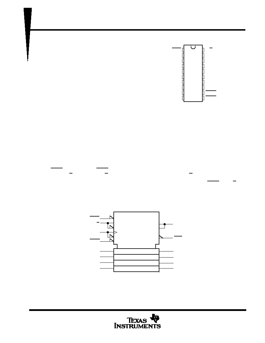
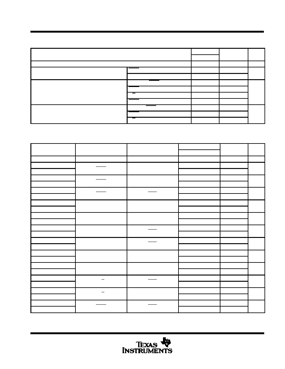
logic symbol
B
12
20
18
13
14
17
11
19
CLK
C
D
A
G1
9
8
3
2
M2 [DOWN]
M3 [UP]
1,2≠/1,3+
G4
C5
6,1,4
3(CT=15)Z6
2(CT=0)Z6
CTRDIV16
RCO
MAX/MIN
10
1
5D
[1]
[2]
[4]
[8]
CTEN
LOAD
D/U
QA
QB
QC
QD
This symbol is in accordance with ANSI/IEEE Std 91-1984
and IEC Publication 617-12.
1
2
3
4
5
6
7
8
9
10
20
19
18
17
16
15
14
13
12
11
RCO
Q
A
Q
B
GND
GND
GND
GND
Q
C
Q
D
MAX/MIN
D/U
CLK
A
B
V
CC
V
CC
C
D
CTEN
LOAD
DW OR N PACKAGE
(TOP VIEW)
EPIC is a trademark of Texas Instruments Incorporated.
PRODUCTION DATA information is current as of publication date.
Products conform to specifications per the terms of Texas Instruments
standard warranty. Production processing does not necessarily include
testing of all parameters.

74ACT11191
SYNCHRONOUS 4-BIT UP/DOWN BINARY COUNTER
SCAS106A ≠ D3455, FEBRUARY 1990 ≠ REVISED APRIL 1993
POST OFFICE BOX 655303
∑
DALLAS, TEXAS 75265
2≠2
description (continued)
These counters are fully programmable; that is, they may be preset to any number between 0 and 15 by placing
a low on the load input and entering the desired data at the data inputs. The outputs will change to agree with
the data inputs independently of the level of the clock input. This feature allows the counter to be used as a
modulo-N divider by simply modifying the count length with the preset inputs.
Two outputs have been made available to perform the cascading function: ripple clock and maximum/minimum
count. The latter output produces a high-level output pulse with a duration approximately equal to one complete
cycle of the clock while the count is zero (all outputs low) counting down or maximum (15) counting up. The
ripple clock output (ROC) produces a low-level output pulse under those same conditions but only while the
clock input is low. The counter can easily be cascaded by feeding the ripple clock output to the enable input
of the succeeding counter if parallel clocking is used, or to the clock input if parallel enabling is used. The
maximum/minimum count output can be used to accomplish look-ahead for high-speed operation.
The 74ACT11191 is characterized for operation from ≠ 40
∞
C to 85
∞
C.
74ACT11191
SYNCHRONOUS 4-BIT UP/DOWN BINARY COUNTER
SCAS106A ≠ D3455, FEBRUARY 1990 ≠ REVISED APRIL 1993
POST OFFICE BOX 655303
∑
DALLAS, TEXAS 75265
2≠3
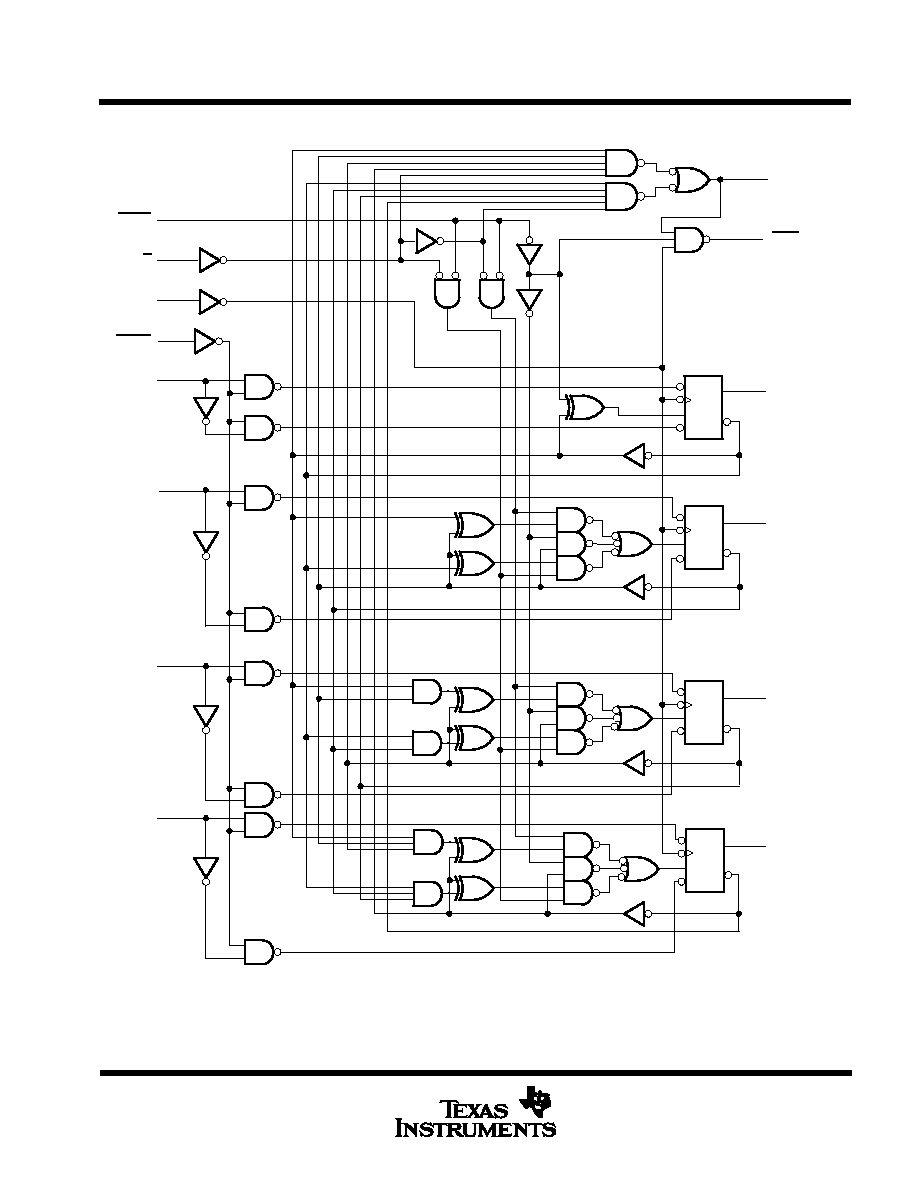
logic diagram (positive logic)
18
12
11
19
20
S
R
RCO
CLK
MAX/MIN
A
17
14
13
S
C1
1D
R
S
C1
1D
R
S
C1
1D
R
B
C
D
10
1
2
3
8
9
CTEN
D/U
LOAD
QB
QC
QD
1D
C1
QA
74ACT11191
SYNCHRONOUS 4-BIT UP/DOWN BINARY COUNTER
SCAS106A ≠ D3455, FEBRUARY 1990 ≠ REVISED APRIL 1993
POST OFFICE BOX 655303
∑
DALLAS, TEXAS 75265
2≠4
typical load, count, and inhibit sequences
Illustrated below is the following sequence:
1.
Load (preset) to binary thirteen
2.
Count up to fourteen, fifteen (maximum), zero, one, and two
3.
Inhibit
4.
Count down to one, zero (minimum), fifteen, fourteen, and thirteen.
A
B
C
D
CLOCK
D/U
MAX/MIN
QA
QD
QC
QB
Load
Count Up
Inhibit
Count Down
13
14
15
0
1
2
2
2
1
0
15
14
13
Data
Inputs
RCO
CTEN
LOAD
74ACT11191
SYNCHRONOUS 4-BIT UP/DOWN BINARY COUNTER
SCAS106A ≠ D3455, FEBRUARY 1990 ≠ REVISED APRIL 1993
POST OFFICE BOX 655303
∑
DALLAS, TEXAS 75265
2≠5
absolute maximum ratings over operating free-air temperature range (unless otherwise noted)
Supply voltage range, V
CC
≠ 0.5 V to 7 V
. . . . . . . . . . . . . . . . . . . . . . . . . . . . . . . . . . . . . . . . . . . . . . . . . . . . . . . . . .
Input voltage range, V
I
(see Note 1)
≠ 0.5 V to V
CC
+ 0.5 V
. . . . . . . . . . . . . . . . . . . . . . . . . . . . . . . . . . . . . . . . . . .
Output voltage range, V
O
(see Note 1)
≠ 0.5 V to V
CC
+ 0.5 V
. . . . . . . . . . . . . . . . . . . . . . . . . . . . . . . . . . . . . . . .
Input clamp current, I
IK
(V
I
< 0 or V
I
> V
CC
)
±
20 mA
. . . . . . . . . . . . . . . . . . . . . . . . . . . . . . . . . . . . . . . . . . . . . . . . .
Output clamp current, I
OK
(V
O
< 0 or V
O
> V
CC
)
±
50 mA
. . . . . . . . . . . . . . . . . . . . . . . . . . . . . . . . . . . . . . . . . . . .
Continuous output current, I
O
(V
O
= 0 to V
CC
)
±
50 mA
. . . . . . . . . . . . . . . . . . . . . . . . . . . . . . . . . . . . . . . . . . . . . .
Continuous current through V
CC
or GND
±
50 mA
. . . . . . . . . . . . . . . . . . . . . . . . . . . . . . . . . . . . . . . . . . . . . . . . . . .
Storage temperature range
≠ 65
∞
C to 150
∞
C
. . . . . . . . . . . . . . . . . . . . . . . . . . . . . . . . . . . . . . . . . . . . . . . . . . . . . . . .
Stresses beyond those listed under "absolute maximum ratings" may cause permanent damage to the device. These are stress ratings only and
functional operation of the device at these or any other conditions beyond those indicated under "recommended operating conditions" is not
implied. Exposure to absolute-maximum-rated conditions for extended periods may affect device reliability.
NOTE 1: The input and output voltage ratings may be exceeded if the input and output current ratings are observed.
recommended operating conditions
MIN
MAX
UNIT
VCC
Supply voltage
4.5
5.5
V
VIH
High-level input voltage
2
V
VIL
Low-level input voltage
0.8
V
VI
Input voltage
0
VCC
V
VO
Output voltage
0
VCC
V
IOH
High-level output current
≠ 24
mA
IOL
Low-level output current
24
mA
D
t /
D
v
Input transition rise or fall rate
0
10
ns/ V
TA
Operating free-air temperature
≠ 40
85
∞
C
electrical characteristics over recommended operating free-air temperature range (unless
otherwise noted)
PARAMETER
TEST CONDITIONS
VCC
TA = 25
∞
C
MIN
MAX
UNIT
PARAMETER
TEST CONDITIONS
VCC
MIN
TYP
MAX
MIN
MAX
UNIT
IOH = 50
m
A
4.5 V
4.4
4.4
IOH = ≠ 50
m
A
5.5 V
5.4
5.4
VOH
IOH = 24 mA
4.5 V
3.94
3.8
V
OH
IOH = ≠ 24 mA
5.5 V
4.94
4.8
IOH = ≠ 75 mA
}
5.5 V
3.85
IOL = 50
m
A
4.5 V
0.1
0.1
IOL = 50
m
A
5.5 V
0.1
0.1
VOL
IOL = 24 mA
4.5 V
0.36
0.44
V
OL
IOL = 24 mA
5.5 V
0.36
0.44
IOL = 75 mA
}
5.5 V
1.65
II
VI = VCC or GND
5.5 V
±
0.1
±
1
m
A
ICC
VI = VCC or GND,
IO = 0
5.5 V
8
80
m
A
D
ICC
w
One input at 3.4 V
Other inputs at GND or VCC
5.5 V
0.9
1
mA
Ci
VI = VCC or GND
5 V
4
pF
Not more than one output should be tested at a time, and the duration of the test should not exceed 10 ms.
ß This is the increase in supply current for each input that is at one of the specified TTL voltage levels rather than 0 V or VCC.
74ACT11191
SYNCHRONOUS 4-BIT UP/DOWN BINARY COUNTER
SCAS106A ≠ D3455, FEBRUARY 1990 ≠ REVISED APRIL 1993
POST OFFICE BOX 655303
∑
DALLAS, TEXAS 75265
2≠6
timing requirements over recommended ranges of supply voltage and operating free-air
temperature (unless otherwise noted) (see Figure 1)
TA = 25
∞
C
MIN
MAX
UNIT
MIN
MAX
MIN
MAX
UNIT
fclock
Clock frequency
0
65
0
65
MHz
t
Pulse duration
LOAD low
4
4
ns
tw
Pulse duration
CLK high or low
7.7
7.7
ns
Data before LOAD
3
3
t
Setup time
CTEN before CLK
7.5
7.5
ns
tsu
Setup time
D/U before CLK
8.5
8.5
ns
LOAD inactive before CLK
2
2
Data after LOAD
2.5
2.5
th
Hold time
CTEN after CLK
1.5
1.5
ns
D/U after CLK
0.5
0.5
switching characteristics over recommended ranges of supply voltage and operating free-air
temperature (unless otherwise noted) (see Figure 1)
PARAMETER
FROM
TO
TA = 25
∞
C
MIN
MAX
UNIT
PARAMETER
(INPUT)
(OUTPUT)
MIN
TYP
MAX
MIN
MAX
UNIT
fmax
65
95
65
MHz
tPLH
LOAD
Any Q
4
7.6
10.8
4
12.2
ns
tPHL
LOAD
Any Q
3.8
7.4
10.5
3.8
11.9
ns
tPLH
LOAD
MAX/MIN
5.2
9.7
13.9
5.2
15.8
ns
tPHL
LOAD
MAX/MIN
4.7
9.5
13.6
4.7
15.4
ns
tPLH
LOAD
RCO
5.4
10.5
15.1
5.4
17.1
ns
tPHL
LOAD
RCO
5.8
11
15.7
5.8
17.9
ns
tPLH
A B C or D
Any Q
4.5
7.6
10.1
4.5
11.6
ns
tPHL
A, B, C, or D
Any Q
3.7
7.1
10.3
3.7
11.7
ns
tPLH
A B C or D
MAX/MIN
5.1
9.5
13.6
5.1
15.4
ns
tPHL
A, B, C, or D
MAX/MIN
4.7
9.2
13.4
4.7
15.2
ns
tPLH
A B C or D
RCO
5.5
10.3
14.8
5.5
17.2
ns
tPHL
A, B, C, or D
RCO
5.9
10.9
15.5
5.9
18
ns
tPLH
CLK
RCO
4.4
7.4
9.5
4.4
11
ns
tPHL
CLK
RCO
3.5
6.7
9.5
3.5
10.8
ns
tPLH
CLK
Any Q
3.6
6.7
9.2
3.6
10.4
ns
tPHL
CLK
Any Q
4.2
7.1
9.4
4.2
10.8
ns
tPLH
CLK
MAX/MIN
5
8
10.3
5
11.7
ns
tPHL
CLK
MAX/MIN
5.3
8.6
11.5
5.3
13.1
ns
tPLH
D/U
RCO
4.4
8.4
11.7
4.4
13.1
ns
tPHL
D/U
RCO
4.2
8.8
11.3
4.2
13
ns
tPLH
D/U
MAX/MIN
3.2
6.9
9.6
3.2
11
ns
tPHL
D/U
MAX/MIN
3.6
7.2
10.3
3.6
11.6
ns
tPLH
CTEN
RCO
3.9
6.4
8.2
3.9
9.2
ns
tPHL
CTEN
RCO
2.8
6
8.4
2.8
9.5
ns
74ACT11191
SYNCHRONOUS 4-BIT UP/DOWN BINARY COUNTER
SCAS106A ≠ D3455, FEBRUARY 1990 ≠ REVISED APRIL 1993
POST OFFICE BOX 655303
∑
DALLAS, TEXAS 75265
2≠7
operating characteristics, V
CC
= 5 V, T
A
= 25
∞
C
PARAMETER
TEST CONDITIONS
TYP
UNIT
Cpd Power dissipation capacitance
CL = 50 pF, f = 1 MHz
68
pF
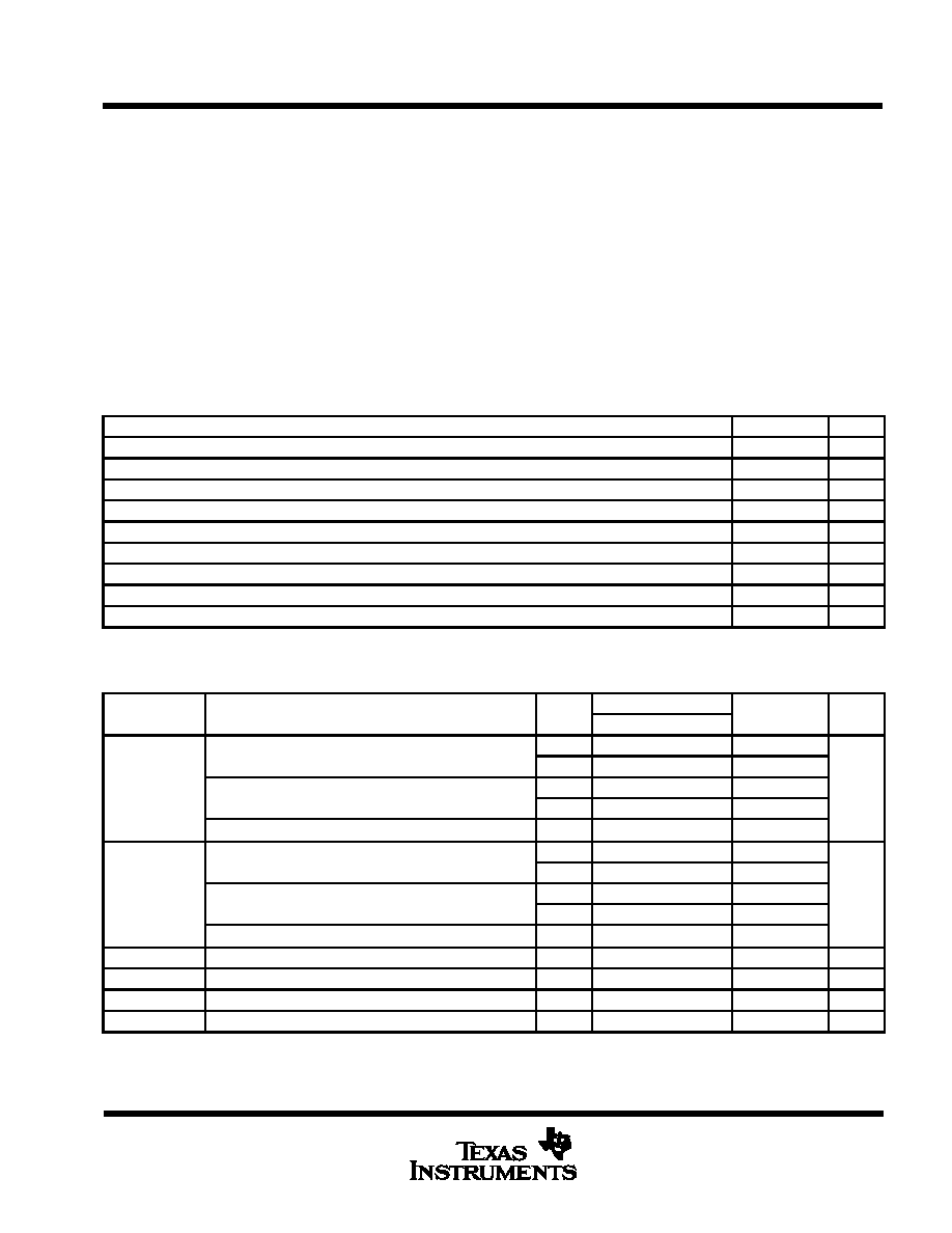
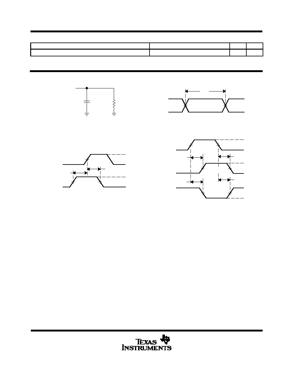
PARAMETER MEASUREMENT INFORMATION
50% VCC
1.5 V
1.5 V
1.5 V
3 V
3 V
0 V
0 V
th
tsu
VOLTAGE WAVEFORMS
Data Input
tPLH
tPHL
tPHL
tPLH
VOH
VOH
VOL
VOL
1.5 V
1.5 V
3 V
0 V
50% VCC
50% VCC
Input
(see Note B)
Out-of-Phase
Output
In-Phase
Output
Timing Input
(see Note B)
50% VCC
VOLTAGE WAVEFORMS
3 V
0 V
1.5 V
1.5 V
tw
VOLTAGE WAVEFORMS
Input
LOAD CIRCUIT
From Output
Under Test
CL = 50 pF
(see Note A)
500
NOTES: A. CL includes probe and jig capacitance.
B. All input pulses are supplied by generators having the following characteristics: PRR
10 MHz, ZO = 50
, tr = 3 ns, tf = 3 ns.
C. The outputs are measured one at a time with one input transition per measurement.
Figure 1. Load Circuit and Voltage Waveforms

74ACT11191
SYNCHRONOUS 4-BIT UP/DOWN BINARY COUNTER
SCAS106A ≠ D3455, FEBRUARY 1990 ≠ REVISED APRIL 1993
POST OFFICE BOX 655303
∑
DALLAS, TEXAS 75265
2≠8

IMPORTANT NOTICE
Texas Instruments and its subsidiaries (TI) reserve the right to make changes to their products or to discontinue
any product or service without notice, and advise customers to obtain the latest version of relevant information
to verify, before placing orders, that information being relied on is current and complete. All products are sold
subject to the terms and conditions of sale supplied at the time of order acknowledgement, including those
pertaining to warranty, patent infringement, and limitation of liability.
TI warrants performance of its semiconductor products to the specifications applicable at the time of sale in
accordance with TI's standard warranty. Testing and other quality control techniques are utilized to the extent
TI deems necessary to support this warranty. Specific testing of all parameters of each device is not necessarily
performed, except those mandated by government requirements.
CERTAIN APPLICATIONS USING SEMICONDUCTOR PRODUCTS MAY INVOLVE POTENTIAL RISKS OF
DEATH, PERSONAL INJURY, OR SEVERE PROPERTY OR ENVIRONMENTAL DAMAGE ("CRITICAL
APPLICATIONS"). TI SEMICONDUCTOR PRODUCTS ARE NOT DESIGNED, AUTHORIZED, OR
WARRANTED TO BE SUITABLE FOR USE IN LIFE-SUPPORT DEVICES OR SYSTEMS OR OTHER
CRITICAL APPLICATIONS. INCLUSION OF TI PRODUCTS IN SUCH APPLICATIONS IS UNDERSTOOD TO
BE FULLY AT THE CUSTOMER'S RISK.
In order to minimize risks associated with the customer's applications, adequate design and operating
safeguards must be provided by the customer to minimize inherent or procedural hazards.
TI assumes no liability for applications assistance or customer product design. TI does not warrant or represent
that any license, either express or implied, is granted under any patent right, copyright, mask work right, or other
intellectual property right of TI covering or relating to any combination, machine, or process in which such
semiconductor products or services might be or are used. TI's publication of information regarding any third
party's products or services does not constitute TI's approval, warranty or endorsement thereof.
Copyright
©
1998, Texas Instruments Incorporated