74ACT11657
OCTAL TRANSCEIVER WITH PARITY GENERATOR/CHECKER
AND 3-STATE OUTPUTS
SCAS232 ≠ AUGUST 1992 ≠ REVISED APRIL 1993
POST OFFICE BOX 655303
∑
DALLAS, TEXAS 75265
Copyright
©
1993, Texas Instruments Incorporated
2≠1
∑
Inputs Are TTL-Voltage Compatible
∑
Flow-Through Architecture Optimizes
PCB Layout
∑
Center-Pin V
CC
and GND Pin
Configurations Minimize High-Speed
Switching Noise
∑
EPIC
TM
(Enhanced-Performance Implanted
CMOS) 1-
µ
m Process
∑
500-mA Typical Latch-Up Immunity
at 125
∞
C
∑
Package Options Include Plastic
Small-Outline Packages and Standard
Plastic 300-mil DIPs
description
The 74ACT11657 contains eight noninverting
buffers with 3-state outputs and an 8-bit parity
generator/checker and is intended for bus-
oriented applications.
The transmit/receive (T/R) input determines the direction of data flow through the bidirectional transceivers.
When T/R is high, data flows from the A port to the B port (transmit mode); when T/R is low, data flows from
the B port to the A port (receive mode). When the output-enable (OE) input is high, both the A and B ports are
in the high-impedance state.
Odd or even parity is selected by a logic high or low level, respectively, on the ODD/EVEN input. PARITY carries
the parity bit value; it is an output from the parity generator/checker in the transmit mode and an input to the parity
generator/checker in the receive mode.
In the transmit mode, after the A bus is polled to determine the number of high bits, PARITY is set to the logic
level that maintains the parity sense selected by the level at the ODD/EVEN input. For example, if ODD/EVEN
is low (even parity selected) and there are five high bits on the A bus, then PARITY is set to the logic high level
so that an even number of the nine total bits (eight A-bus bits plus parity bit) are high.
In the receive mode, after the B bus is polled to determine the number of high bits, the ERR output logic level
indicates whether or not the data to be received exhibits the correct parity sense. For example, if ODD/EVEN
is high (odd parity selected), PARITY is high, and there are three high bits on the B bus, then ERR is low,
indicating a parity error.
The 74ACT11657 is characterized for operation from ≠ 40
∞
C to 85
∞
C.
PRODUCTION DATA information is current as of publication date.
Products conform to specifications per the terms of Texas Instruments
standard warranty. Production processing does not necessarily include
testing of all parameters.
EPIC is a trademark of Texas Instruments Incorporated.
1
2
3
4
5
6
7
8
9
10
11
12
13
14
28
27
26
25
24
23
22
21
20
19
18
17
16
15
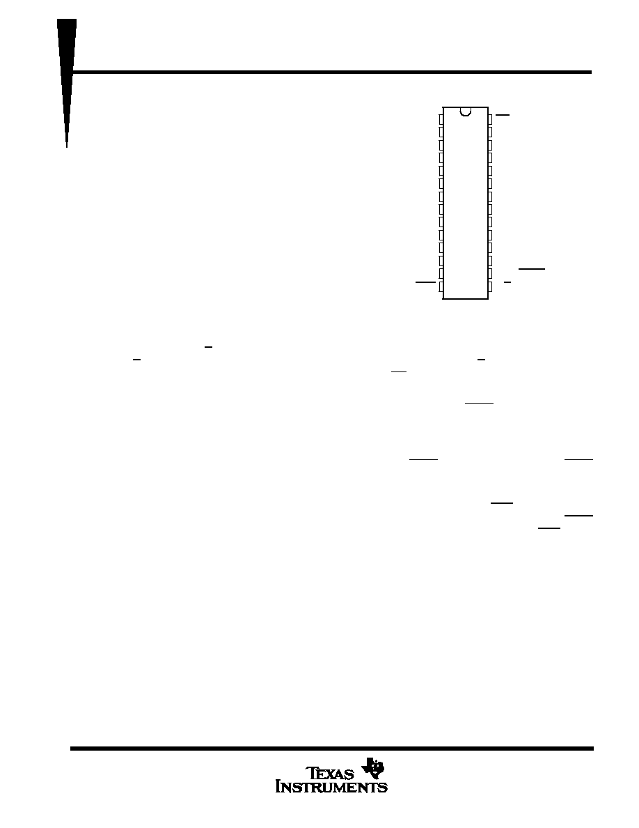
PARITY
A1
A2
A3
A4
GND
GND
GND
GND
A5
A6
A7
A8
ERR
OE
B1
B2
B3
B4
V
CC
V
CC
V
CC
B5
B6
B7
B8
ODD/EVEN
T/R
DW PACKAGE
(TOP VIEW)
74ACT11657
OCTAL TRANSCEIVER WITH PARITY GENERATOR/CHECKER
AND 3-STATE OUTPUTS
SCAS232 ≠ AUGUST 1992 ≠ REVISED APRIL 1993
POST OFFICE BOX 655303
∑
DALLAS, TEXAS 75265
2≠2
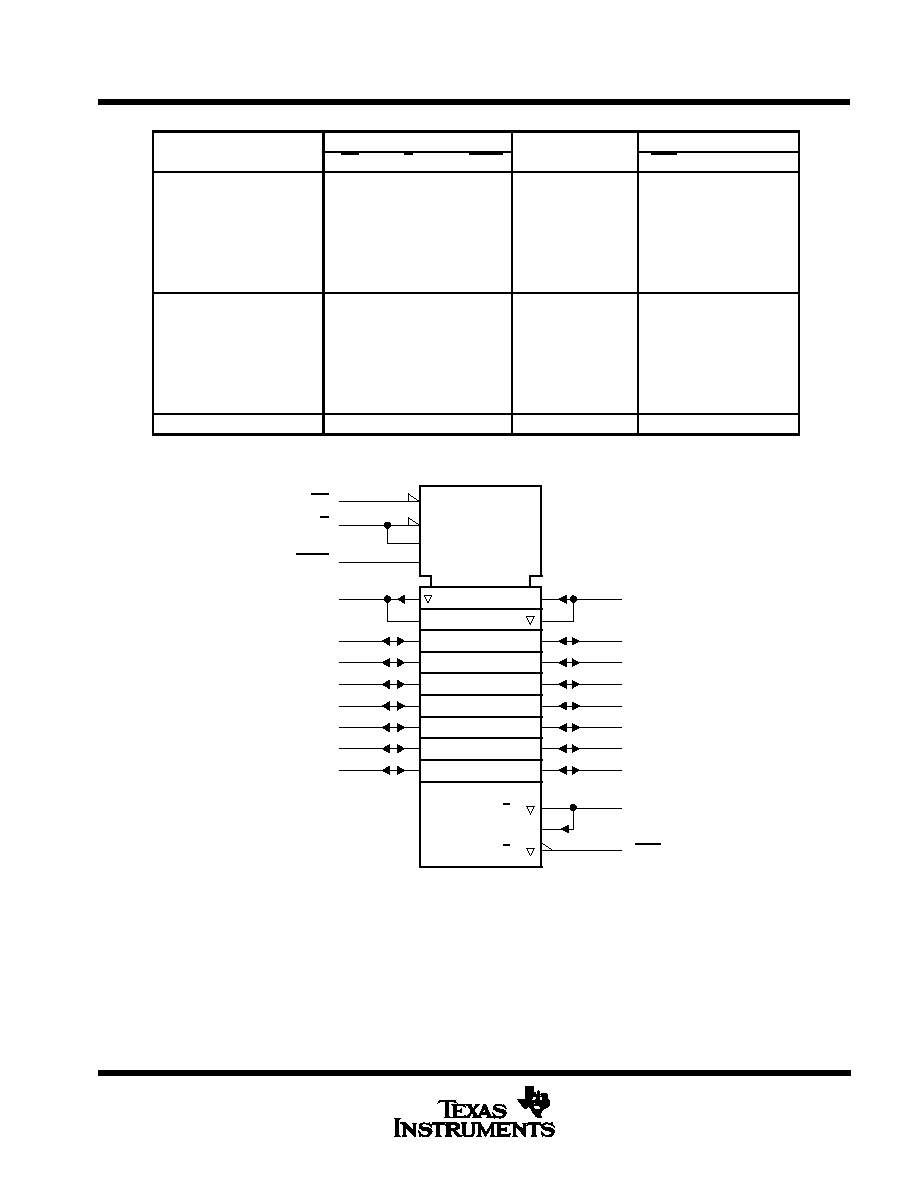
FUNCTION TABLE
NUMBER OF A OR B
INPUTS
INPUT/OUTPUT
OUTPUTS
NUMBER OF A OR B
INPUTS THAT ARE HIGH
OE
T/R
ODD/EVEN
INPUT/OUTPUT
PARITY
ERR
OUTPUT MODE
L
H
H
H
Z
Transmit
L
H
L
L
Z
Transmit
0 2 4 6 8
L
L
H
H
H
Receive
0, 2, 4, 6, 8
L
L
H
L
L
Receive
L
L
L
H
L
Receive
L
L
L
L
H
Receive
L
H
H
L
Z
Transmit
L
H
L
H
Z
Transmit
1 3 5 7
L
L
H
H
L
Receive
1, 3, 5, 7
L
L
H
L
H
Receive
L
L
L
H
H
Receive
L
L
L
L
L
Receive
Don't care
H
X
X
Z
Z
Z
logic symbol
OE
A1
2
A2
3
A3
4
A4
5
A5
10
A6
11
A7
12
A8
13
G3
28
3 EN1/3G5 [REC]
15
3 EN2 [XMIT]
N4
55
B1
27
B2
26
B3
25
B4
24
B5
20
B6
19
B7
18
B8
17
PARITY
1
5
14
T/R
ODD/EVEN
ERR
1
2
2k
4, 2
4, 1
1
1
This symbol is in accordance with ANSI/IEEE Std 91-1984 and IEC Publication 617-12.
74ACT11657
OCTAL TRANSCEIVER WITH PARITY GENERATOR/CHECKER
AND 3-STATE OUTPUTS
SCAS232 ≠ AUGUST 1992 ≠ REVISED APRIL 1993
POST OFFICE BOX 655303
∑
DALLAS, TEXAS 75265
2≠3
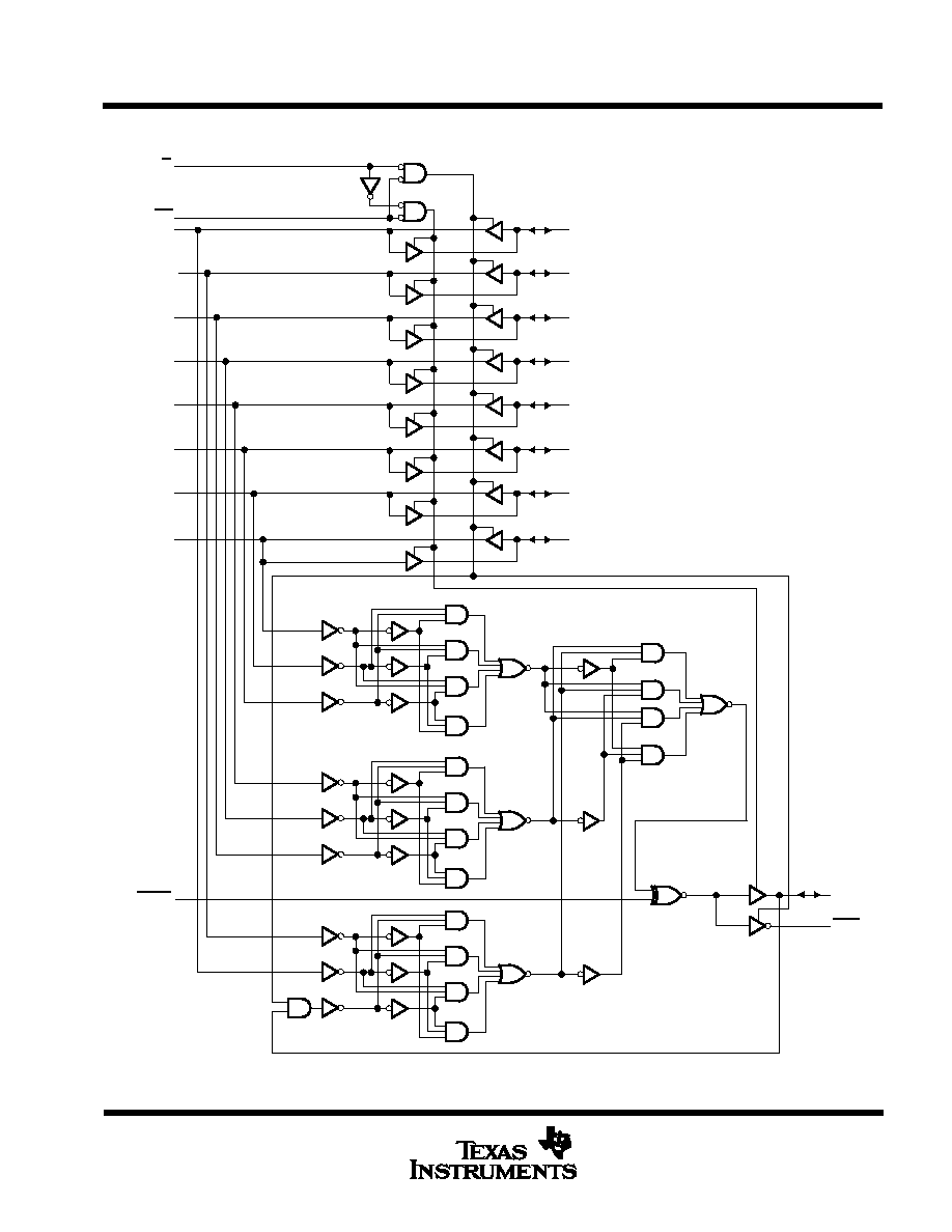
logic diagram (positive logic)
T/R
OE
ERR
A1
A2
A3
A4
A5
A6
A7
A8
ODD/EVEN
PARITY
B2
B3
B4
B5
B6
B7
B8
B1
15
28
2
3
4
5
10
11
12
13
16
1
14
27
26
25
24
20
19
18
17
74ACT11657
OCTAL TRANSCEIVER WITH PARITY GENERATOR/CHECKER
AND 3-STATE OUTPUTS
SCAS232 ≠ AUGUST 1992 ≠ REVISED APRIL 1993
POST OFFICE BOX 655303
∑
DALLAS, TEXAS 75265
2≠4
absolute maximum ratings over operating free-air temperature range (unless otherwise noted)
Supply voltage range, V
CC
≠ 0.5 V to 7 V
. . . . . . . . . . . . . . . . . . . . . . . . . . . . . . . . . . . . . . . . . . . . . . . . . . . . . . . . . .
Input voltage range, V
I
(see Note 1)
≠ 0.5 V to V
CC
+ 0.5 V
. . . . . . . . . . . . . . . . . . . . . . . . . . . . . . . . . . . . . . . . . .
Output voltage range, V
O
(see Note 1)
≠ 0.5 V to V
CC
+ 0.5 V
. . . . . . . . . . . . . . . . . . . . . . . . . . . . . . . . . . . . . . .
Input clamp current, I
IK
(V
I
< 0 or V
I
> V
CC
)
±
20 mA
. . . . . . . . . . . . . . . . . . . . . . . . . . . . . . . . . . . . . . . . . . . . . . .
Output clamp current, I
OK
(V
O
< 0 or V
O
> V
CC
)
±
50 mA
. . . . . . . . . . . . . . . . . . . . . . . . . . . . . . . . . . . . . . . . . . .
Continuous output current, I
O
(V
O
= 0 to V
CC
)
±
50 mA
. . . . . . . . . . . . . . . . . . . . . . . . . . . . . . . . . . . . . . . . . . . . .
Continuous current through V
CC
or GND
±
225 mA
. . . . . . . . . . . . . . . . . . . . . . . . . . . . . . . . . . . . . . . . . . . . . . . . .
Storage temperature range
≠ 65
∞
C to 150
∞
C
. . . . . . . . . . . . . . . . . . . . . . . . . . . . . . . . . . . . . . . . . . . . . . . . . . . . . . .
Stresses beyond those listed under "absolute maximum ratings" may cause permanent damage to the device. These are stress ratings only, and
functional operation of the device at these or any other conditions beyond those indicated under "recommended operating conditions" is not
implied. Exposure to absolute-maximum-rated conditions for extended periods may affect device reliability.
NOTE 1: The input and output voltage ratings may be exceeded if the input and output clamp-current ratings are observed.
recommended operating conditions (see Note 2)
MIN
NOM
MAX
UNIT
VCC
Supply voltage
4.5
5
5.5
V
VIH
High-level input voltage
2
V
VIL
Low-level input voltage
0.8
V
VI
Input voltage
0
VCC
V
VO
Output voltage
0
VCC
V
IOH
High-level output current
≠ 24
mA
IOL
Low-level output current
24
mA
t /
v
Input transition rise or fall rate
0
10
ns/ V
TA
Operating free-air temperature
≠ 40
85
∞
C
NOTE 2: Unused or floating pins (input or I/O) must be held high or low.
74ACT11657
OCTAL TRANSCEIVER WITH PARITY GENERATOR/CHECKER
AND 3-STATE OUTPUTS
SCAS232 ≠ AUGUST 1992 ≠ REVISED APRIL 1993
POST OFFICE BOX 655303
∑
DALLAS, TEXAS 75265
2≠5
electrical characteristics over recommended operating free-air temperature range (unless
otherwise noted)
PARAMETER
TEST CONDITIONS
VCC
TA = 25
∞
C
MIN
MAX
UNIT
PARAMETER
TEST CONDITIONS
VCC
MIN
TYP
MAX
MIN
MAX
UNIT
IOH = 50
µ
A
4.5 V
4.4
4.4
IOH = ≠ 50
µ
A
5.5 V
5.4
5.4
VOH
IOH = 24 mA
4.5 V
3.94
3.8
V
IOH = ≠ 24 mA
5.5 V
4.94
4.8
IOH = ≠ 75 mA
5.5 V
3.85
IOL = 50
µ
A
4.5 V
0.1
0.1
IOL = 50
µ
A
5.5 V
0.1
0.1
VOL
IOL = 24 mA
4.5 V
0.36
0.44
V
IOL = 24 mA
5.5 V
0.36
0.44
IOL = 75 mA
5.5 V
1.65
II
A or B ports
VI = VCC or GND
5.5 V
±
0.1
±
1
µ
A
IOZ
Control Inputs
VO = VCC or GND
5.5 V
±
0.5
±
5
µ
A
ICC
VI = VCC or GND, IO = 0
5.5 V
8
80
µ
A
ICCß
One input at 3.4 V, Other inputs at VCC or GND
5.5 V
0.9
1
mA
Ci
Control inputs
VI = VCC or GND
5 V
4.5
pF
Co
PARITY/ERR
VO = VCC or GND
5 V
10
pF
Cio
A or B ports
VO = VCC or GND
5 V
12
pF
Not more than one output should be tested at a time, and the duration of the test should not exceed 10 ms.
For I/O ports, the parameter IOZ includes the input leakage current.
ß This is the increase in supply current for each input that is at one of the specified TTL voltage levels rather than 0 V or VCC.
switching characteristics over recommended operating free-air temperature range,
V
CC
= 5 V
±
0.5 V (unless otherwise noted) (see Figure 1)
PARAMETER
FROM
TO
TA = 25
∞
C
MIN
MAX
UNIT
PARAMETER
(INPUT)
(OUTPUT)
MIN
TYP
MAX
MIN
MAX
UNIT
tPLH
A or B
B or A
2.9
6.7
8.4
2.9
9.4
ns
tPHL
A or B
B or A
2.2
7
8.4
2.2
9.4
ns
tPLH
A
PARITY
3.4
10.4
12.7
3.4
14.4
ns
tPHL
A
PARITY
3.9
10.9
13.2
3.9
15
ns
tPLH
ODD/EVEN
PARITY ERR
2.5
7.9
9.4
2.5
10.7
ns
tPHL
ODD/EVEN
PARITY, ERR
3
8.5
10
3
11.3
ns
tPLH
B
ERR
4.6
18.1
20.6
4.6
23.6
ns
tPHL
B
ERR
4.9
18.5
21.8
4.9
24.6
ns
tPLH
PARITY
ERR
4
10.9
12.8
4
14.6
ns
tPHL
PARITY
ERR
3.9
11
12.9
3.9
14.7
ns
tPZH
OE
A B PARITY or ERR
2.6
9.1
10.8
2.6
12.1
ns
tPZL
OE
A, B, PARITY, or ERR
3.1
10.6
12.3
3.1
13.8
ns
tPHZ
OE
A B PARITY or ERR
4.5
9.1
10.8
4.5
12.1
ns
tPLZ
OE
A, B, PARITY, or ERR
4.5
8.7
10.5
4.5
11.6
ns
74ACT11657
OCTAL TRANSCEIVER WITH PARITY GENERATOR/CHECKER
AND 3-STATE OUTPUTS
SCAS232 ≠ AUGUST 1992 ≠ REVISED APRIL 1993
POST OFFICE BOX 655303
∑
DALLAS, TEXAS 75265
2≠6
operating characteristics, V
CC
= 5 V, T
A
= 25
∞
C
PARAMETER
TEST CONDITIONS
TYP
UNIT
Cpd
Power dissipation capacitance per transceiver
Outputs enabled
CL = 50 pF
f = 1 MHz
95
pF
Cpd
Power dissi ation ca acitance er transceiver
Outputs disabled
CL = 50 F, f = 1 MHz
21
F
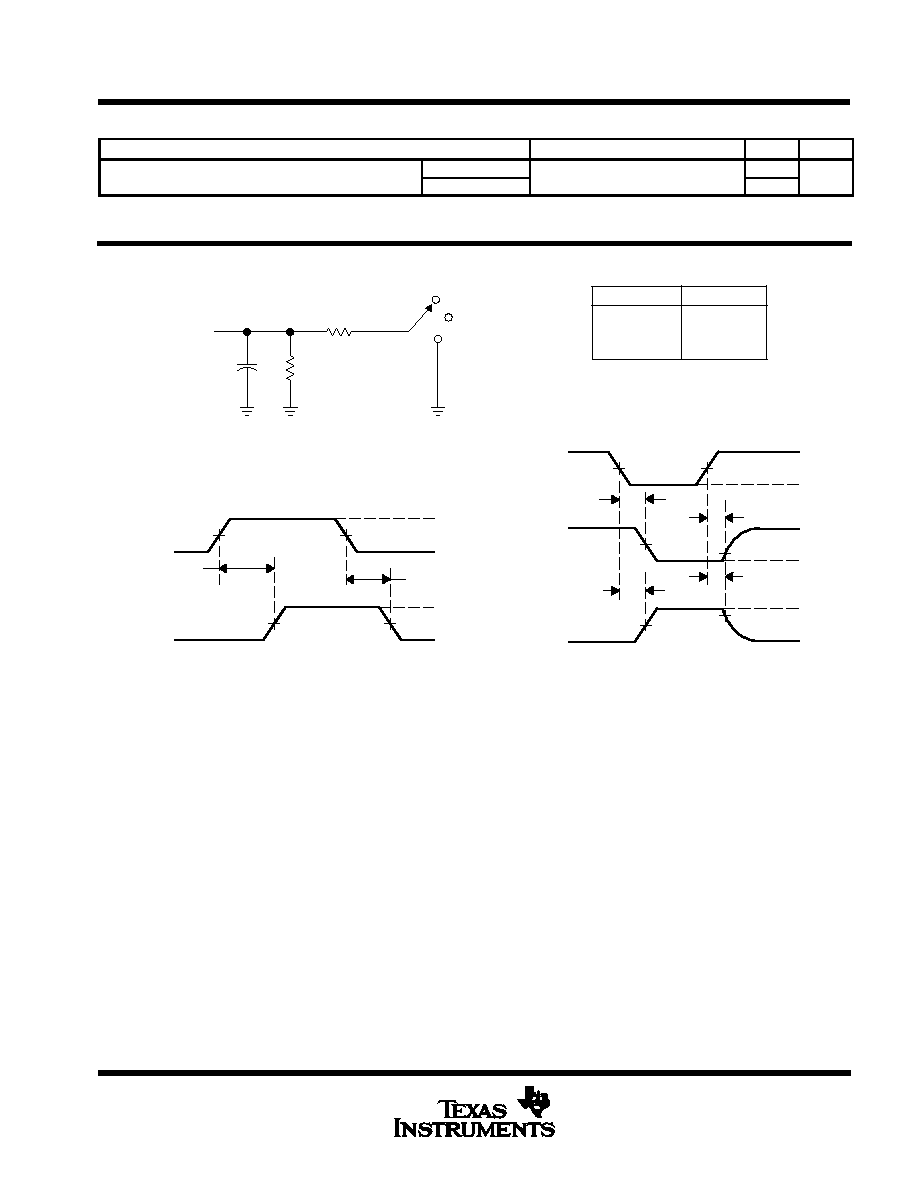
PARAMETER MEASUREMENT INFORMATION
From Output
Under Test
CL = 50 pF
(see Note A)
LOAD CIRCUIT
S1
2
◊
VCC
500
500
tPLH
tPHL
Output
Control
(low-level
enabling)
Output
Waveform 1
S1 at 2
◊
VCC
(see Note C)
Output
Waveform 2
S1 at GND
(see Note C)
VOL
VOH
tPZL
tPZH
tPLZ
tPHZ
1.5 V
1.5 V
1.5 V
1.5 V
VCC
3 V
0 V
50% VCC
50% VCC
VOH
VOL
0 V
50% VCC
20% VCC
50% VCC
80% VCC
0 V
3 V
GND
Open
Input
(see Note B)
Output
VOLTAGE WAVEFORMS
VOLTAGE WAVEFORMS
tPLH/tPHL
tPLZ/tPZL
tPHZ/tPZH
Open
2
◊
VCC
GND
TEST
S1
NOTES: A. CL includes probe and jig capacitance.
B. All input pulses are supplied by generators having the following characteristics: PRR
10 MHz, ZO = 50
, tr = 3 ns, tf = 3 ns.
C. Waveform 1 is for an output with internal conditions such that the output is low except when disabled by the output control.
Waveform 2 is for an output with internal conditions such that the output is high except when disabled by the output control.
D. The outputs are measured one at a time with one input transition per measurement.
Figure 1. Load Circuit and Voltage Waveforms

IMPORTANT NOTICE
Texas Instruments and its subsidiaries (TI) reserve the right to make changes to their products or to discontinue
any product or service without notice, and advise customers to obtain the latest version of relevant information
to verify, before placing orders, that information being relied on is current and complete. All products are sold
subject to the terms and conditions of sale supplied at the time of order acknowledgement, including those
pertaining to warranty, patent infringement, and limitation of liability.
TI warrants performance of its semiconductor products to the specifications applicable at the time of sale in
accordance with TI's standard warranty. Testing and other quality control techniques are utilized to the extent
TI deems necessary to support this warranty. Specific testing of all parameters of each device is not necessarily
performed, except those mandated by government requirements.
CERTAIN APPLICATIONS USING SEMICONDUCTOR PRODUCTS MAY INVOLVE POTENTIAL RISKS OF
DEATH, PERSONAL INJURY, OR SEVERE PROPERTY OR ENVIRONMENTAL DAMAGE ("CRITICAL
APPLICATIONS"). TI SEMICONDUCTOR PRODUCTS ARE NOT DESIGNED, AUTHORIZED, OR
WARRANTED TO BE SUITABLE FOR USE IN LIFE-SUPPORT DEVICES OR SYSTEMS OR OTHER
CRITICAL APPLICATIONS. INCLUSION OF TI PRODUCTS IN SUCH APPLICATIONS IS UNDERSTOOD TO
BE FULLY AT THE CUSTOMER'S RISK.
In order to minimize risks associated with the customer's applications, adequate design and operating
safeguards must be provided by the customer to minimize inherent or procedural hazards.
TI assumes no liability for applications assistance or customer product design. TI does not warrant or represent
that any license, either express or implied, is granted under any patent right, copyright, mask work right, or other
intellectual property right of TI covering or relating to any combination, machine, or process in which such
semiconductor products or services might be or are used. TI's publication of information regarding any third
party's products or services does not constitute TI's approval, warranty or endorsement thereof.
Copyright
©
1998, Texas Instruments Incorporated