54ACT16821, 74ACT16821
20-BIT BUS-INTERFACE FLIP-FLOPS
WITH 3-STATE OUTPUTS
SCAS176A ≠ JANUARY 1991 ≠ REVISED APRIL 1996
1
POST OFFICE BOX 655303
∑
DALLAS, TEXAS 75265
D
Members of the Texas Instruments
Widebus
TM
Family
D
Inputs Are TTL-Voltage Compatible
D
Provide Extra Data Width Necessary for
Wider Address/Data Paths or Buses With
Parity
D
Flow-Through Architecture Optimizes
PCB Layout
D
Distributed V
CC
and GND Pin Configuration
Minimizes High-Speed Switching Noise
D
EPIC
TM
(Enhanced-Performance Implanted
CMOS) 1-
µ
m Process
D
Package Options Include 300-mil Shrink
Small-Outline (DL) Packages Using 25-mil
Center-to-Center Pin Spacings and 380-mil
Fine-Pitch Ceramic Flat (WD) Packages
Using 25-mil Center-to-Center Pin Spacings
description
These 20-bit flip-flops feature 3-state outputs
designed specifically for driving highly-capacitive
or relatively low-impedance loads. They are
particularly suitable for implementing wider buffer
registers, I/O ports, parity bus interfacing, and
working registers.
The 'ACT16821 can be used as two 10-bit
flip-flops or one 20-bit flip-flop. On the positive
transition of the clock (CLK) input, the Q outputs
follow the data (D) inputs. Each 10-bit flip-flop
section has a buffered output-enable (1OE or
2OE) input that can be used to place the ten
outputs in either a normal logic state (high or low
logic levels) or the high-impedance state. In the
high-impedance state, the outputs neither load
nor drive the bus lines significantly.
OE does not affect the internal operation of the flip-flops. Old data can be retained or new data can be entered
while the outputs are in the high-impedance state.
The 74ACT16821 is packaged in theTI shrink small-outline package, which provides twice the I/O pin count and
functionality of standard small-outline packages in the same printed-circuit-board area.
The 54ACT16821 is characterized for operation over the full military temperature range of ≠55
∞
C to 125
∞
C. The
74ACT16821 is characterized for operation from ≠40
∞
C to 85
∞
C.
Copyright
©
1996, Texas Instruments Incorporated
UNLESS OTHERWISE NOTED this document contains PRODUCTION
DATA information current as of publication date. Products conform to
specifications per the terms of Texas Instruments standard warranty.
Production processing does not necessarily include testing of all
parameters.
Please be aware that an important notice concerning availability, standard warranty, and use in critical applications of
Texas Instruments semiconductor products and disclaimers thereto appears at the end of this data sheet.
EPIC and Widebus are trademarks of Texas Instruments Incorporated.
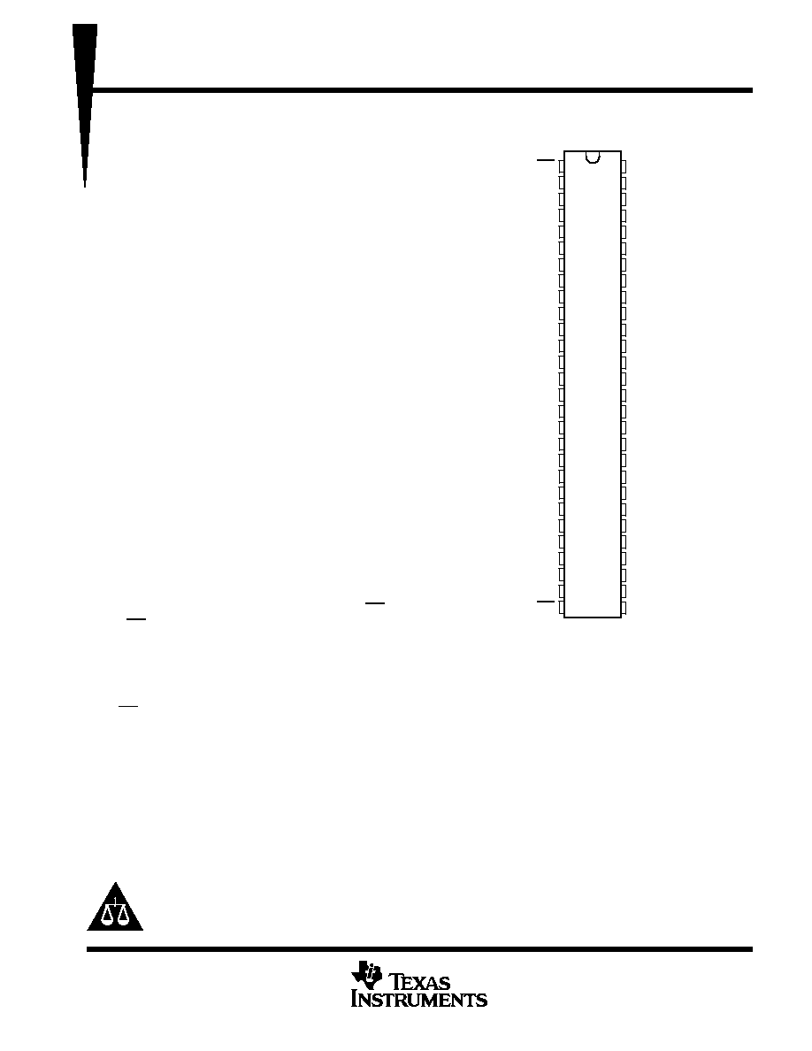
54ACT16821 . . . WD PACKAGE
74ACT16821 . . . DL PACKAGE
(TOP VIEW)
1
2
3
4
5
6
7
8
9
10
11
12
13
14
15
16
17
18
19
20
21
22
23
24
25
26
27
28
56
55
54
53
52
51
50
49
48
47
46
45
44
43
42
41
40
39
38
37
36
35
34
33
32
31
30
29
1OE
1Q1
1Q2
GND
1Q3
1Q4
V
CC
1Q5
1Q6
1Q7
GND
1Q8
1Q9
1Q10
2Q1
2Q2
2Q3
GND
2Q4
2Q5
2Q6
V
CC
2Q7
2Q8
GND
2Q9
2Q10
2OE
1CLK
1D1
1D2
GND
1D3
1D4
V
CC
1D5
1D6
1D7
GND
1D8
1D9
1D10
2D1
2D2
2D3
GND
2D4
2D5
2D6
V
CC
2D7
2D8
GND
2D9
2D10
2CLK
54ACT16821, 74ACT16821
20-BIT BUS-INTERFACE FLIP-FLOPS
WITH 3-STATE OUTPUTS
SCAS176A ≠ JANUARY 1991 ≠ REVISED APRIL 1996
2
POST OFFICE BOX 655303
∑
DALLAS, TEXAS 75265
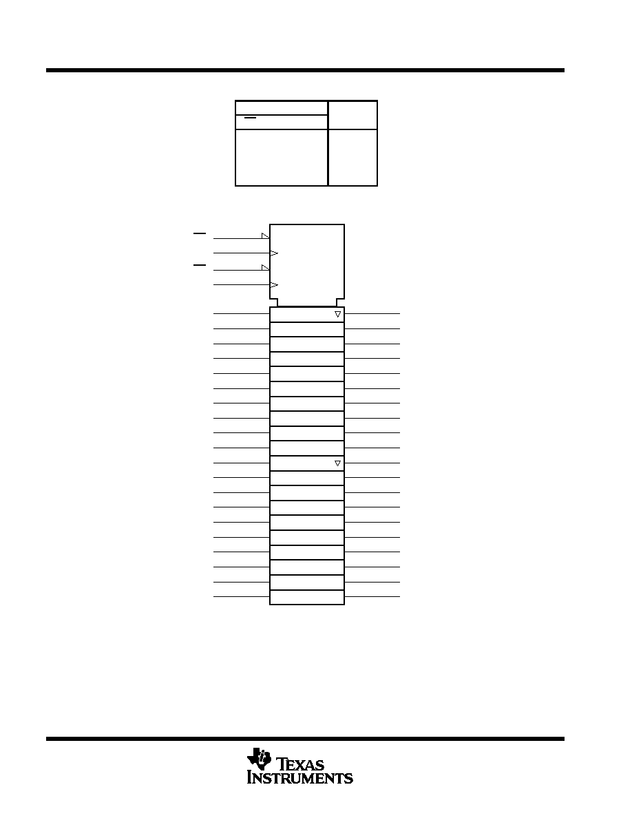
FUNCTION TABLE
(each 10-bit flip-flop)
INPUTS
OUTPUT
OE
CLK
D
Q
L
H
H
L
L
L
L
H or L
X
Q0
H
X
X
Z
logic symbol
1Q1
2
1Q2
3
1Q3
5
1Q4
6
1Q5
8
1Q6
9
1Q7
10
1Q8
12
1Q9
13
1Q10
14
2Q1
15
2Q2
16
2Q3
17
2Q4
19
2Q5
20
2Q6
21
2Q7
23
2Q8
24
2Q9
26
2Q10
27
1OE
EN2
1
56
1CLK
1D
55
1D1
54
1D2
52
1D3
51
1D4
49
1D5
48
1D6
47
1D7
45
1D8
44
1D9
43
1D10
3D
42
2D1
41
2D2
40
2D3
38
2D4
37
2D5
36
2D6
34
2D7
33
2D8
31
2D9
30
2D10
EN4
28
29
2CLK
2OE
C1
C3
2
4
This symbol is in accordance with ANSI/IEEE Std 91-1984 and IEC Publication 617-12.
54ACT16821, 74ACT16821
20-BIT BUS-INTERFACE FLIP-FLOPS
WITH 3-STATE OUTPUTS
SCAS176A ≠ JANUARY 1991 ≠ REVISED APRIL 1996
3
POST OFFICE BOX 655303
∑
DALLAS, TEXAS 75265
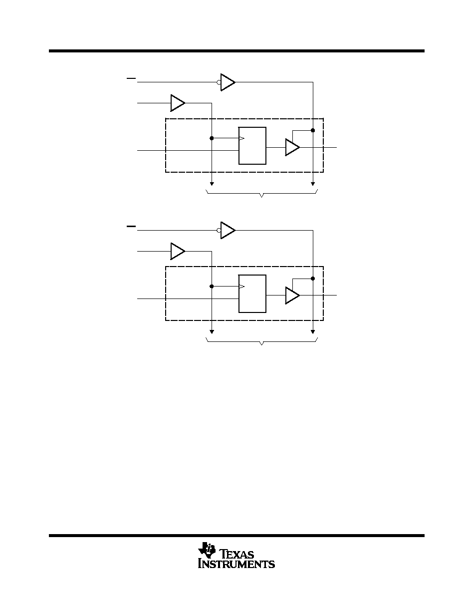
logic diagram (positive logic)
1D1
1OE
55
1
56
1Q1
2
1CLK
1D
To Nine Other Channels
C1
One of Ten
Channels
2D1
2OE
42
28
29
2Q1
15
2CLK
1D
To Nine Other Channels
C1
One of Ten
Channels
absolute maximum ratings over operating free-air temperature range (unless otherwise noted)
Supply voltage range, V
CC
≠0.5 V to 7 V
. . . . . . . . . . . . . . . . . . . . . . . . . . . . . . . . . . . . . . . . . . . . . . . . . . . . . . . . . .
Input voltage range, V
I
(see Note 1)
≠0.5 V to V
CC
+ 0.5 V
. . . . . . . . . . . . . . . . . . . . . . . . . . . . . . . . . . . . . . . . . . .
Output voltage range, V
O
(see Note 1)
≠0.5 V to V
CC
+ 0.5 V
. . . . . . . . . . . . . . . . . . . . . . . . . . . . . . . . . . . . . . . .
Input clamp current, I
IK
(V
I
< 0 or V
I
> V
CC
)
±
20 mA
. . . . . . . . . . . . . . . . . . . . . . . . . . . . . . . . . . . . . . . . . . . . . . . .
Output clamp current, I
OK
(V
O
< 0 or V
O
> V
CC
)
±
50 mA
. . . . . . . . . . . . . . . . . . . . . . . . . . . . . . . . . . . . . . . . . . . .
Continuous output current, I
O
(V
O
= 0 to V
CC
)
±
50 mA
. . . . . . . . . . . . . . . . . . . . . . . . . . . . . . . . . . . . . . . . . . . . . .
Continuous current through V
CC
or GND
±
500 mA
. . . . . . . . . . . . . . . . . . . . . . . . . . . . . . . . . . . . . . . . . . . . . . . . . .
Maximum package power dissipation at T
A
= 55
∞
C (in still air) (see Note 2): DL package
1.4 W
. . . . . . . . . . .
Storage temperature range, T
stg
≠65
∞
C to 150
∞
C
. . . . . . . . . . . . . . . . . . . . . . . . . . . . . . . . . . . . . . . . . . . . . . . . . . .
Stresses beyond those listed under "absolute maximum ratings" may cause permanent damage to the device. These are stress ratings only, and
functional operation of the device at these or any other conditions beyond those indicated under "recommended operating conditions" is not
implied. Exposure to absolute-maximum-rated conditions for extended periods may affect device reliability.
NOTES:
1. The input and output voltage ratings may be exceeded if the input and output current ratings are observed.
2. The maximum package power dissipation is calculated using a junction temperature of 150
∞
C and a board trace length of 750 mils.
54ACT16821, 74ACT16821
20-BIT BUS-INTERFACE FLIP-FLOPS
WITH 3-STATE OUTPUTS
SCAS176A ≠ JANUARY 1991 ≠ REVISED APRIL 1996
4
POST OFFICE BOX 655303
∑
DALLAS, TEXAS 75265
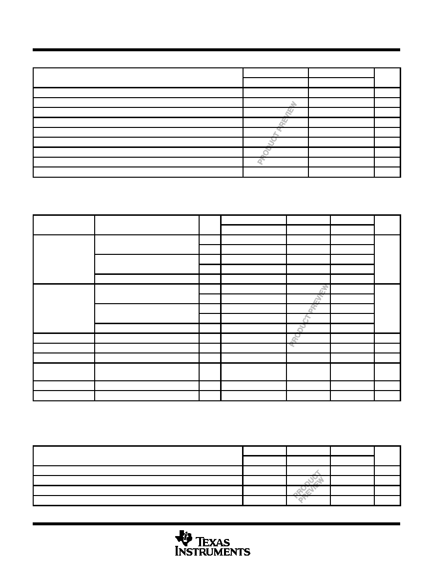
recommended operating conditions (see Note 3)
54ACT16821
74ACT16821
UNIT
MIN
NOM
MAX
MIN
NOM
MAX
UNIT
VCC
Supply voltage
4.5
5
5.5
4.5
5
5.5
V
VIH
High-level input voltage
2
2
V
VIL
Low-level input voltage
0.8
0.8
V
VI
Input voltage
0
VCC
0
VCC
V
VO
Output voltage
0
VCC
0
VCC
V
IOH
High-level output current
≠24
≠24
mA
IOL
Low-level output current
24
24
mA
t/
v
Input transition rise or fall rate
0
10
0
10
ns/V
TA
Operating free-air temperature
≠55
125
≠40
85
∞
C
NOTE 3: Unused inputs must be held high or low to prevent them from floating.
electrical characteristics over recommended operating free-air temperature range (unless
otherwise noted)
PARAMETER
TEST CONDITIONS
VCC
TA = 25
∞
C
54ACT16821
74ACT16821
UNIT
PARAMETER
TEST CONDITIONS
VCC
MIN
TYP
MAX
MIN
MAX
MIN
MAX
UNIT
IOH = 50
µ
A
4.5 V
4.4
4.4
4.4
IOH = ≠50
µ
A
5.5 V
5.4
5.4
5.4
VOH
IOH = 24 mA
4.5 V
3.94
3.8
3.8
V
IOH = ≠24 mA
5.5 V
4.94
4.8
4.8
IOH = ≠75 mA
5.5 V
3.85
3.85
IOL = 50
µ
A
4.5 V
0.1
0.1
0.1
IOL = 50
µ
A
5.5 V
0.1
0.1
0.1
VOL
IOL = 24 mA
4.5 V
0.36
0.44
0.44
V
IOL = 24 mA
5.5 V
0.36
0.44
0.44
IOL = 75 mA
5.5 V
1.65
1.65
II
VI = VCC or GND
5.5 V
±
0.1
±
1
±
1
µ
A
IOZ
VO = VCC or GND
5.5 V
±
0.5
±
5
±
5
µ
A
ICC
VI = VCC or GND,
IO = 0
5.5 V
8
80
80
µ
A
ICC
One input at 3.4 V,
Other inputs at VCC or GND
5.5 V
0.9
1
1
mA
Ci
VI = VCC or GND
5 V
3
pF
Ci
VO = VCC or GND
5 V
11
pF
Not more than one output should be tested at a time, and the duration of the test should not exceed 10 ms.
This is the increase in supply current for each input that is at one of the specified TTL voltage levels rather than 0 V or VCC.
timing requirements over recommended operating free-air temperature range,
V
CC
= 5 V
±
0.5 V (unless otherwise noted) (see Figure 1)
TA = 25
∞
C
54ACT16821
74ACT16821
UNIT
MIN
MAX
MIN
MAX
MIN
MAX
UNIT
fclock
Clock frequency
0
70
0
70
0
70
MHz
tw
Pulse duration, CLK high or low
7
7
7
ns
tsu
Setup time, data before CLK
7.5
7.5
7.5
ns
th
Hold time, data after CLK
0.5
0.5
0.5
ns
PRODUCT PREVIEW information concerns products in the formative or
design phase of development. Characteristic data and other
specifications are design goals. Texas Instruments reserves the right to
change or discontinue these products without notice.
54ACT16821, 74ACT16821
20-BIT BUS-INTERFACE FLIP-FLOPS
WITH 3-STATE OUTPUTS
SCAS176A ≠ JANUARY 1991 ≠ REVISED APRIL 1996
5
POST OFFICE BOX 655303
∑
DALLAS, TEXAS 75265
switching characteristics over recommended operating free-air temperature range,
V
CC
= 5 V
±
0.5 V (unless otherwise noted) (see Figure 1)
PARAMETER
FROM
TO
TA = 25
∞
C
54ACT16821
74ACT16821
UNIT
PARAMETER
(INPUT)
(OUTPUT)
MIN
TYP
MAX
MIN
MAX
MIN
MAX
UNIT
fmax
70
70
70
MHz
tPLH
CLK
Any Q
4.5
8.8
12
4.5
13.4
4.5
13.4
ns
tPHL
CLK
Any Q
5.2
9.5
12.6
5.2
14
5.2
14
ns
tPZH
OE
Any Q
2.8
8.6
10.8
2.8
11.9
2.8
11.9
ns
tPZL
OE
Any Q
4
9.7
13.3
4
14.7
4
14.7
ns
tPHZ
OE
Any Q
5.4
8.3
10
5.4
10.7
5.4
10.7
ns
tPLZ
OE
Any Q
4.7
7.6
9.3
4.7
10
4.7
10
ns
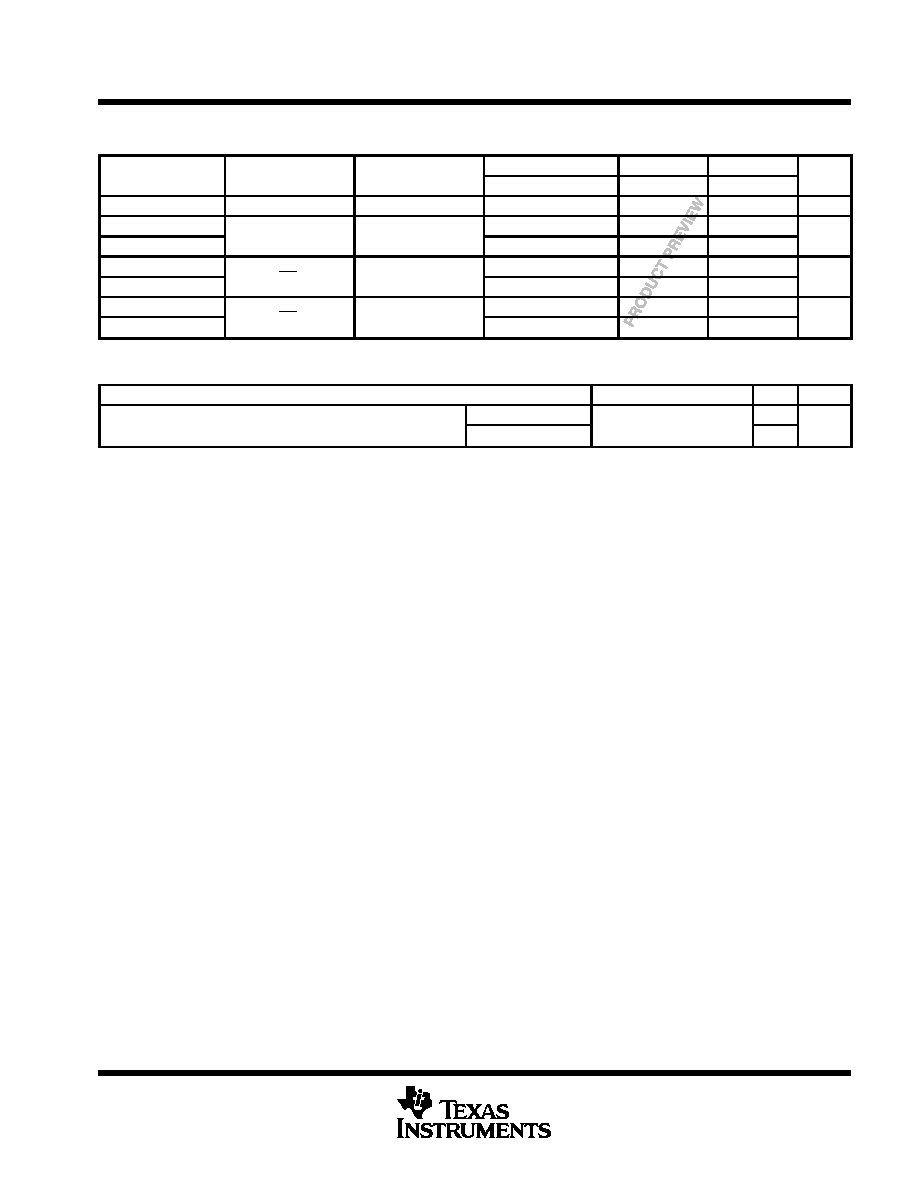
operating characteristics, V
CC
= 5 V, T
A
= 25
∞
C
PARAMETER
TEST CONDITIONS
TYP
UNIT
C d
Power dissipation capacitance per flip flop
Outputs enabled
CL = 50 pF
f = 1 MHz
41
pF
Cpd
Power dissipation capacitance per flip-flop
Outputs disabled
CL = 50 pF,
f = 1 MHz
25
pF
PRODUCT PREVIEW information concerns products in the formative or
design phase of development. Characteristic data and other
specifications are design goals. Texas Instruments reserves the right to
change or discontinue these products without notice.