www.ti.com
FEATURES
DESCRIPTION/ORDERING INFORMATION
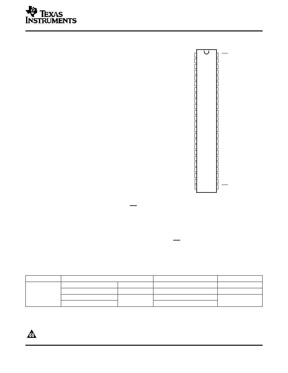
DGG OR DL PACKAGE
(TOP VIEW)
1
2
3
4
5
6
7
8
9
10
11
12
13
14
15
16
17
18
19
20
21
22
23
24
48
47
46
45
44
43
42
41
40
39
38
37
36
35
34
33
32
31
30
29
28
27
26
25
1DIR
1B1
1B2
GND
1B3
1B4
V
CC
1B5
1B6
GND
1B7
1B8
2B1
2B2
GND
2B3
2B4
V
CC
2B5
2B6
GND
2B7
2B8
2DIR
1OE
1A1
1A2
GND
1A3
1A4
V
CC
1A5
1A6
GND
1A7
1A8
2A1
2A2
GND
2A3
2A4
V
CC
2A5
2A6
GND
2A7
2A8
2OE
SN74ALVCHR16245
16-BIT BUS TRANSCEIVER
WITH 3-STATE OUTPUTS
SCES064G ≠ DECEMBER 1995 ≠ REVISED OCTOBER 2004
∑
Member of the Texas Instruments WidebusTM
Family
∑
Operates From 1.65 V to 3.6 V
∑
Max t
pd
of 4.2 ns at 3.3 V
∑
±
12-mA Output Drive at 3.3 V
∑
All Outputs Have Equivalent 26-
Series
Resistors, So No External Resistors Are
Required
∑
Bus Hold on Data Inputs Eliminates the Need
for External Pullup/Pulldown Resistors
∑
Latch-Up Performance Exceeds 250 mA Per
JESD 17
∑
ESD Protection Exceeds JESD 22
- 2000-V Human-Body Model (A114-A)
- 200-V Machine Model (A115-A)
This 16-bit (dual-octal) noninverting bus transceiver is
designed for 1.65-V to 3.6-V V
CC
operation.
The
SN74ALVCHR16245
is
designed
for
asynchronous communication between data buses.
The
control-function
implementation
minimizes
external timing requirements.
This device can be used as two 8-bit transceivers or
one 16-bit transceiver. It allows data transmission
from the A bus to the B bus or from the B bus to the
A
bus,
depending
on
the
logic
level
at
the
direction-control (DIR) input. The output-enable (OE)
input can be used to disable the device so that the
buses are effectively isolated.
All outputs, which are designed to sink up to 12 mA, include equivalent 26-
series resistors to reduce overshoot
and undershoot.
To ensure the high-impedance state during power up or power down, OE should be tied to V
CC
through a pullup
resistor; the minimum value of the resistor is determined by the current-sinking capability of the driver.
Active bus-hold circuitry holds unused or undriven inputs at a valid logic state. Use of pullup or pulldown resistors
with the bus-hold circuitry is not recommended.
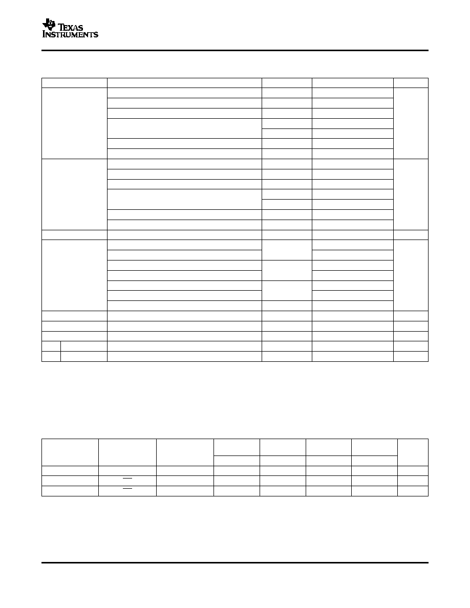
ORDERING INFORMATION
T
A
PACKAGE
(1)
ORDERABLE PART NUMBER
TOP-SIDE MARKING
SSOP - DL
Tape and reel
SN74ALVCHR16245LR
ALVCHR16245
TSSOP - DGG
Tape and reel
SN74ALVCHR16245GR
ALVCHR16245
-40
∞
C to 85
∞
C
VFBGA - GQL
SN74ALVCHR16245KR
Tape and reel
VR245
VFBGA - ZQL (Pb-free)
74ALVCHR16245ZQLR
(1)
Package drawings, standard packing quantities, thermal data, symbolization, and PCB design guidelines are available at
www.ti.com/sc/package.
Please be aware that an important notice concerning availability, standard warranty, and use in critical applications of Texas
Instruments semiconductor products and disclaimers thereto appears at the end of this data sheet.
Widebus is a trademark of Texas Instruments.
PRODUCTION DATA information is current as of publication date.
Copyright © 1995≠2004, Texas Instruments Incorporated
Products conform to specifications per the terms of the Texas
Instruments standard warranty. Production processing does not
necessarily include testing of all parameters.
www.ti.com
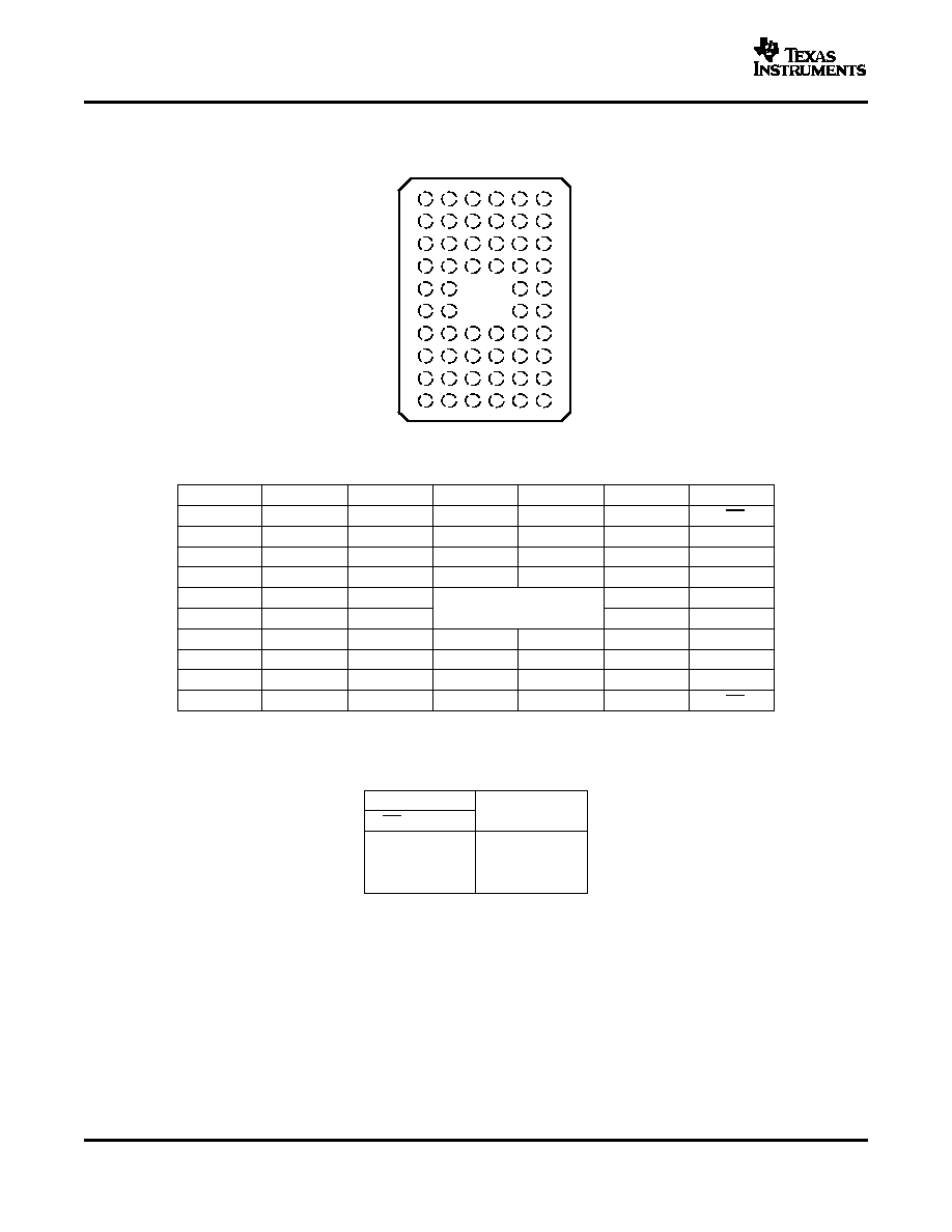
GQL OR ZQL PACKAGE
(TOP VIEW)
J
H
G
F
E
D
C
B
A
2
1
3
4
6
5
K
SN74ALVCHR16245
16-BIT BUS TRANSCEIVER
WITH 3-STATE OUTPUTS
SCES064G ≠ DECEMBER 1995 ≠ REVISED OCTOBER 2004
TERMINAL ASSIGNMENTS
(1)
1
2
3
4
5
6
A
1DIR
NC
NC
NC
NC
1OE
B
1B2
1B1
GND
GND
1A1
1A2
C
1B4
1B3
V
CC
V
CC
1A3
1A4
D
1B6
1B5
GND
GND
1A5
1A6
E
1B8
1B7
1A7
1A8
F
2B1
2B2
2A2
2A1
G
2B3
2B4
GND
GND
2A4
2A3
H
2B5
2B6
V
CC
V
CC
2A6
2A5
J
2B7
2B8
GND
GND
2A8
2A7
K
2DIR
NC
NC
NC
NC
2OE
(1)
NC - No internal connection
FUNCTION TABLE
(each 8-bit section)
INPUTS
OPERATION
OE
DIR
L
L
B data to A bus
L
H
A data to B bus
H
X
Isolation
2
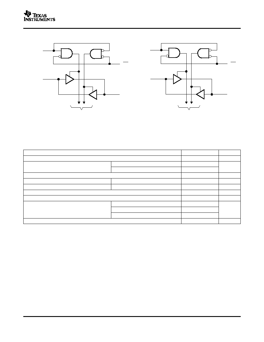
www.ti.com
To Seven Other Channels
1DIR
1A1
1B1
1OE
To Seven Other Channels
2DIR
2A1
2B1
2OE
1
47
24
36
48
2
25
13
Pin numbers shown are for the DGG and DL packages.
ABSOLUTE MAXIMUM RATINGS
(1)
SN74ALVCHR16245
16-BIT BUS TRANSCEIVER
WITH 3-STATE OUTPUTS
SCES064G ≠ DECEMBER 1995 ≠ REVISED OCTOBER 2004
LOGIC DIAGRAM (POSITIVE LOGIC)
over operating free-air temperature range (unless otherwise noted)
MIN
MAX
UNIT
V
CC
Supply voltage range
-0.5
4.6
V
Except I/O ports
(2)
-0.5
4.6
V
I
Input voltage range
V
I/O ports
(2) (3)
-0.5
V
CC
+ 0.5
V
O
Output voltage range
(2) (3)
-0.5
V
CC
+ 0.5
V
I
IK
Input clamp current
V
I
< 0
-50
mA
I
OK
Output clamp current
V
O
< 0
-50
mA
I
O
Continuous output current
±
50
mA
Continuous current through each V
CC
or GND
±
100
mA
DGG package
70
JA
Package thermal impedance
(4)
DL package
63
∞
C/W
GQL/ZQL package
42
T
stg
Storage temperature range
-65
150
∞
C
(1)
Stresses beyond those listed under "absolute maximum ratings" may cause permanent damage to the device. These are stress ratings
only, and functional operation of the device at these or any other conditions beyond those indicated under "recommended operating
conditions" is not implied. Exposure to absolute-maximum-rated conditions for extended periods may affect device reliability.
(2)
The input negative-voltage and output voltage ratings may be exceeded if the input and output current ratings are observed.
(3)
This value is limited to 4.6 V maximum.
(4)
The package thermal impedance is calculated in accordance with JESD 51-7.
3
www.ti.com
RECOMMENDED OPERATING CONDITIONS
(1)
SN74ALVCHR16245
16-BIT BUS TRANSCEIVER
WITH 3-STATE OUTPUTS
SCES064G ≠ DECEMBER 1995 ≠ REVISED OCTOBER 2004
MIN
MAX
UNIT
V
CC
Supply voltage
1.65
3.6
V
V
CC
= 1.65 V to 1.95 V
0.65
◊
V
CC
V
IH
High-level input voltage
V
CC
= 2.3 V to 2.7 V
1.7
V
V
CC
= 2.7 V to 3.6 V
2
V
CC
= 1.65 V to 1.95 V
0.35
◊
V
CC
V
IL
Low-level input voltage
V
CC
= 2.3 V to 2.7 V
0.7
V
V
CC
= 2.7 V to 3.6 V
0.8
V
I
Input voltage
0
V
CC
V
V
O
Output voltage
0
V
CC
V
V
CC
= 1.65 V
-2
V
CC
= 2.3 V
-6
I
OH
High-level output current
mA
V
CC
= 2.7 V
-8
V
CC
= 3 V
-12
V
CC
= 1.65 V
2
V
CC
= 2.3 V
6
I
OL
Low-level output current
mA
V
CC
= 2.7 V
8
V
CC
= 3 V
12
t/
v
Input transition rise or fall rate
10
ns/V
T
A
Operating free-air temperature
-40
85
∞
C
(1)
All unused control inputs of the device must be held at V
CC
or GND to ensure proper device operation. Refer to the TI application report,
Implications of Slow or Floating CMOS Inputs, literature number SCBA004.
4
www.ti.com
ELECTRICAL CHARACTERISTICS
SWITCHING CHARACTERISTICS
SN74ALVCHR16245
16-BIT BUS TRANSCEIVER
WITH 3-STATE OUTPUTS
SCES064G ≠ DECEMBER 1995 ≠ REVISED OCTOBER 2004
over recommended operating free-air temperature range (unless otherwise noted)
PARAMETER
TEST CONDITIONS
V
CC
MIN TYP
(1)
MAX
UNIT
I
OH
= -100
µ
A
1.65 V to 3.6 V
V
CC
- 0.2
I
OH
= -2 mA
1.65 V
1.2
I
OH
= -4 mA
2.3 V
1.9
V
OH
2.3 V
1.7
V
I
OH
= -6 mA
3 V
2.4
I
OH
= -8 mA
2.7 V
2
I
OH
= -12 mA
3 V
2
I
OL
= 100
µ
A
1.65 V to 3.6 V
0.2
I
OL
= 2 mA
1.65 V
0.45
I
OL
= 4 mA
2.3 V
0.4
V
OL
2.3 V
0.55
V
I
OL
= 6 mA
3 V
0.55
I
OL
= 8 mA
2.7 V
0.6
I
OL
= 12 mA
3 V
0.8
I
I
V
I
= V
CC
or GND
3.6 V
±
5
µ
A
V
I
= 0.58 V
25
1.65 V
V
I
= 1.07 V
-25
V
I
= 0.7 V
45
2.3 V
I
I(hold)
V
I
= 1.7 V
-45
µ
A
V
I
= 0.8 V
75
3 V
V
I
= 2 V
-75
V
I
= 0 to 3.6 V
(2)
3.6 V
±
500
I
OZ
(3)
V
O
= V
CC
or GND
3.6 V
±
10
µ
A
I
CC
V
I
= V
CC
or GND,
I
O
= 0
3.6 V
40
µ
A
I
CC
One input at V
CC
- 0.6 V, Other inputs at V
CC
or GND
3 V to 3.6 V
750
µ
A
C
i
Control inputs
V
I
= V
CC
or GND
3.3 V
4
pF
C
io
A or B ports
V
O
= V
CC
or GND
3.3 V
9
pF
(1)
All typical values are at V
CC
= 3.3 V, T
A
= 25
∞
C.
(2)
This is the bus-hold maximum dynamic current. It is the minimum overdrive current required to switch the input from one state to
another.
(3)
For I/O ports, the parameter I
OZ
includes the input leakage current.
over recommended operating free-air temperature range (unless otherwise noted) (see Figure 1)
V
CC
= 2.5 V
V
CC
= 3.3 V
V
CC
= 1.8 V
V
CC
= 2.7 V
FROM
TO
±
0.2 V
±
0.3 V
PARAMETER
UNIT
(INPUT)
(OUTPUT)
TYP
MIN
MAX
MIN
MAX
MIN
MAX
t
pd
A or B
B or A
(1)
1
4.9
4.7
1
4.2
ns
t
en
OE
B or A
(1)
1
6.8
6.7
1
5.6
ns
t
dis
OE
B or A
(1)
1
6.3
5.7
1
5.5
ns
(1)
This information was not available at the time of publication.
5

www.ti.com
OPERATING CHARACTERISTICS
SN74ALVCHR16245
16-BIT BUS TRANSCEIVER
WITH 3-STATE OUTPUTS
SCES064G ≠ DECEMBER 1995 ≠ REVISED OCTOBER 2004
T
A
= 25
∞
C
V
CC
= 1.8 V
V
CC
= 2.5 V
V
CC
= 3.3 V
PARAMETER
TEST CONDITIONS
UNIT
TYP
TYP
TYP
Outputs enabled
(1)
24
32
Power dissipation
C
pd
C
L
= 50 pF,
f = 10 MHz
pF
capacitance
Outputs disabled
(1)
4
5
(1)
This information was not available at the time of publication.
6
www.ti.com
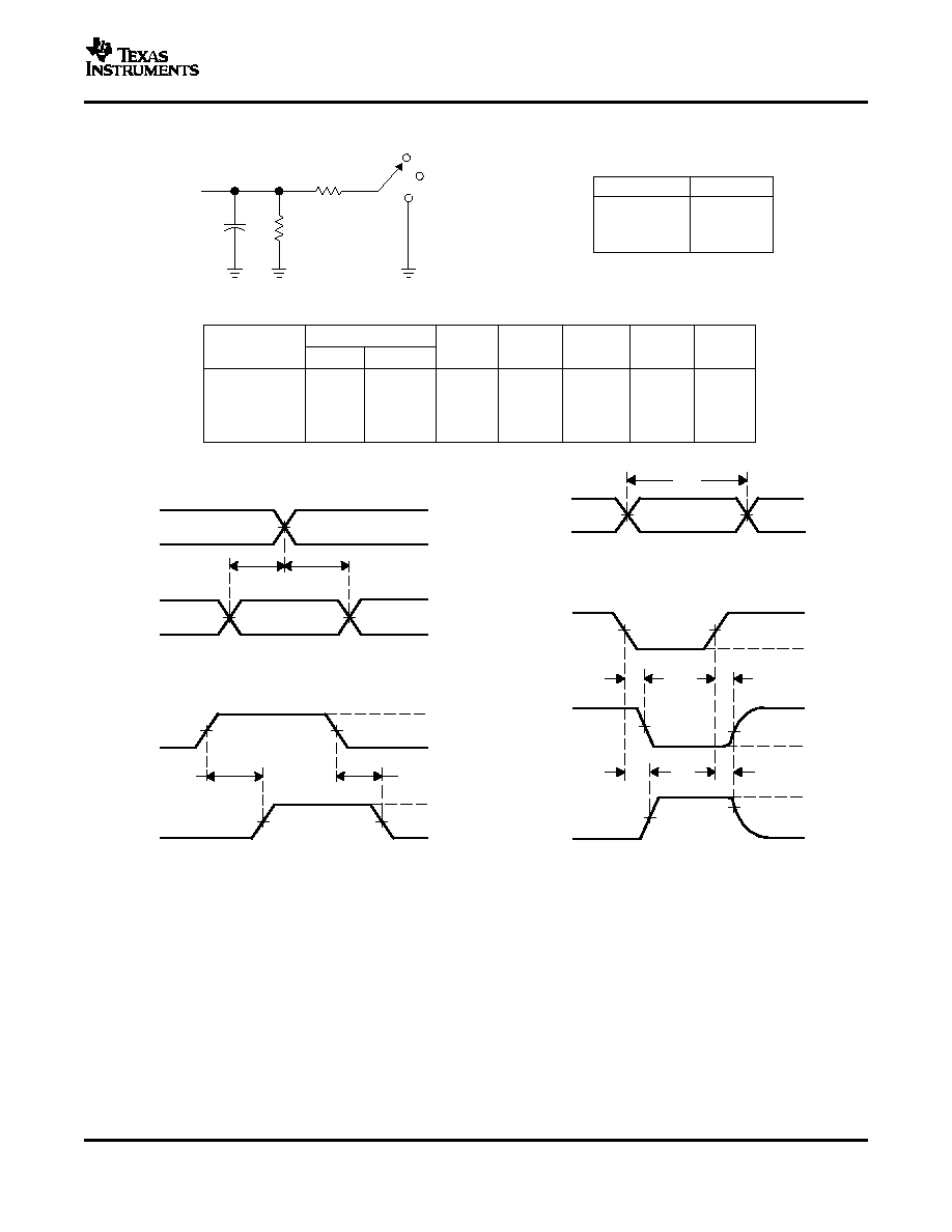
PARAMETER MEASUREMENT INFORMATION
V
M
V
M
V
M
V
M
V
M
V
M
V
M
V
M
V
OH
V
OL
t
h
t
su
From Output
Under Test
C
L
(see Note A)
LOAD CIRCUIT
S1
Open
GND
R
L
R
L
Output
Control
(low-level
enabling)
Output
Waveform 1
S1 at V
LOAD
(see Note B)
Output
Waveform 2
S1 at GND
(see Note B)
t
PZL
t
PZH
t
PLZ
t
PHZ
0 V
V
OL
+ V
V
OH
- V
0 V
V
I
0 V
0 V
t
w
V
I
V
I
VOLTAGE WAVEFORMS
SETUP AND HOLD TIMES
VOLTAGE WAVEFORMS
PULSE DURATION
VOLTAGE WAVEFORMS
ENABLE AND DISABLE TIMES
Timing
Input
Data
Input
Input
t
pd
t
PLZ
/t
PZL
t
PHZ
/t
PZH
Open
V
LOAD
GND
TEST
S1
NOTES: A. C
L
includes probe and jig capacitance.
B. Waveform 1 is for an output with internal conditions such that the output is low, except when disabled by the output control.
Waveform 2 is for an output with internal conditions such that the output is high, except when disabled by the output control.
C. All input pulses are supplied by generators having the following characteristics: PRR
10 MHz, Z
O
= 50
.
D. The outputs are measured one at a time, with one transition per measurement.
E. t
PLZ
and t
PHZ
are the same as t
dis
.
F. t
PZL
and t
PZH
are the same as t
en
.
G. t
PLH
and t
PHL
are the same as t
pd
.
H. All parameters and waveforms are not applicable to all devices.
0 V
V
I
V
M
t
PHL
V
M
V
M
V
I
0 V
V
OH
V
OL
Input
Output
VOLTAGE WAVEFORMS
PROPAGATION DELAY TIMES
V
M
V
M
t
PLH
V
LOAD
V
LOAD
/2
1.8 V
2.5 V
±
0.2 V
2.7 V
3.3 V
±
0.3 V
1 k
500
500
500
V
CC
R
L
2
◊
V
CC
2
◊
V
CC
6 V
6 V
V
LOAD
C
L
30 pF
30 pF
50 pF
50 pF
0.15 V
0.15 V
0.3 V
0.3 V
V
V
CC
V
CC
2.7 V
2.7 V
V
I
V
CC
/2
V
CC
/2
1.5 V
1.5 V
V
M
t
r
/t
f
2 ns
2 ns
2.5 ns
2.5 ns
INPUT
SN74ALVCHR16245
16-BIT BUS TRANSCEIVER
WITH 3-STATE OUTPUTS
SCES064G ≠ DECEMBER 1995 ≠ REVISED OCTOBER 2004
Figure 1. Load Circuit and Voltage Waveforms
7
PACKAGING INFORMATION
Orderable Device
Status
(1)
Package
Type
Package
Drawing
Pins Package
Qty
Eco Plan
(2)
Lead/Ball Finish
MSL Peak Temp
(3)
74ALVCHR16245GRE4
ACTIVE
TSSOP
DGG
48
2000 Green (RoHS &
no Sb/Br)
CU NIPDAU
Level-1-260C-UNLIM
74ALVCHR16245LRG4
ACTIVE
SSOP
DL
48
1000 Green (RoHS &
no Sb/Br)
CU NIPDAU
Level-1-260C-UNLIM
74ALVCHR16245ZQLR
ACTIVE
VFBGA
ZQL
56
1000 Green (RoHS &
no Sb/Br)
SNAGCU
Level-1-260C-UNLIM
SN74ALVCHR16245GR
ACTIVE
TSSOP
DGG
48
2000 Green (RoHS &
no Sb/Br)
CU NIPDAU
Level-1-260C-UNLIM
SN74ALVCHR16245KR
ACTIVE
VFBGA
GQL
56
1000
TBD
SNPB
Level-1-240C-UNLIM
SN74ALVCHR16245LR
ACTIVE
SSOP
DL
48
1000 Green (RoHS &
no Sb/Br)
CU NIPDAU
Level-1-260C-UNLIM
(1)
The marketing status values are defined as follows:
ACTIVE: Product device recommended for new designs.
LIFEBUY: TI has announced that the device will be discontinued, and a lifetime-buy period is in effect.
NRND: Not recommended for new designs. Device is in production to support existing customers, but TI does not recommend using this part in
a new design.
PREVIEW: Device has been announced but is not in production. Samples may or may not be available.
OBSOLETE: TI has discontinued the production of the device.
(2)
Eco
Plan
-
The
planned
eco-friendly
classification:
Pb-Free
(RoHS)
or
Green
(RoHS
&
no
Sb/Br)
-
please
check
http://www.ti.com/productcontent
for the latest availability information and additional product content details.
TBD: The Pb-Free/Green conversion plan has not been defined.
Pb-Free (RoHS): TI's terms "Lead-Free" or "Pb-Free" mean semiconductor products that are compatible with the current RoHS requirements
for all 6 substances, including the requirement that lead not exceed 0.1% by weight in homogeneous materials. Where designed to be soldered
at high temperatures, TI Pb-Free products are suitable for use in specified lead-free processes.
Green (RoHS & no Sb/Br): TI defines "Green" to mean Pb-Free (RoHS compatible), and free of Bromine (Br) and Antimony (Sb) based flame
retardants (Br or Sb do not exceed 0.1% by weight in homogeneous material)
(3)
MSL, Peak Temp. -- The Moisture Sensitivity Level rating according to the JEDEC industry standard classifications, and peak solder
temperature.
Important Information and Disclaimer:The information provided on this page represents TI's knowledge and belief as of the date that it is
provided. TI bases its knowledge and belief on information provided by third parties, and makes no representation or warranty as to the
accuracy of such information. Efforts are underway to better integrate information from third parties. TI has taken and continues to take
reasonable steps to provide representative and accurate information but may not have conducted destructive testing or chemical analysis on
incoming materials and chemicals. TI and TI suppliers consider certain information to be proprietary, and thus CAS numbers and other limited
information may not be available for release.
In no event shall TI's liability arising out of such information exceed the total purchase price of the TI part(s) at issue in this document sold by TI
to Customer on an annual basis.
PACKAGE OPTION ADDENDUM
www.ti.com
4-Oct-2005
Addendum-Page 1
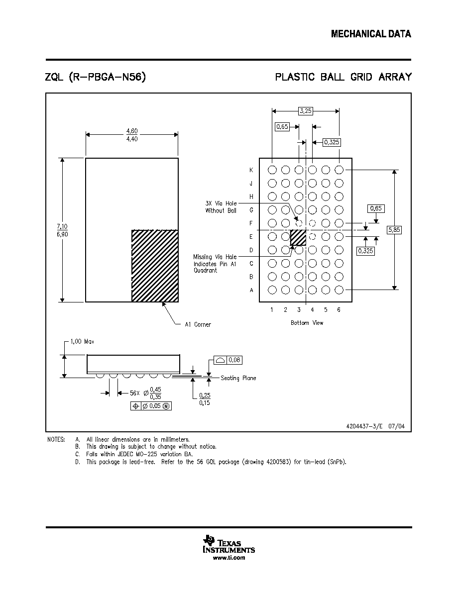
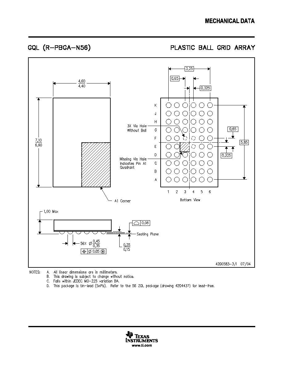
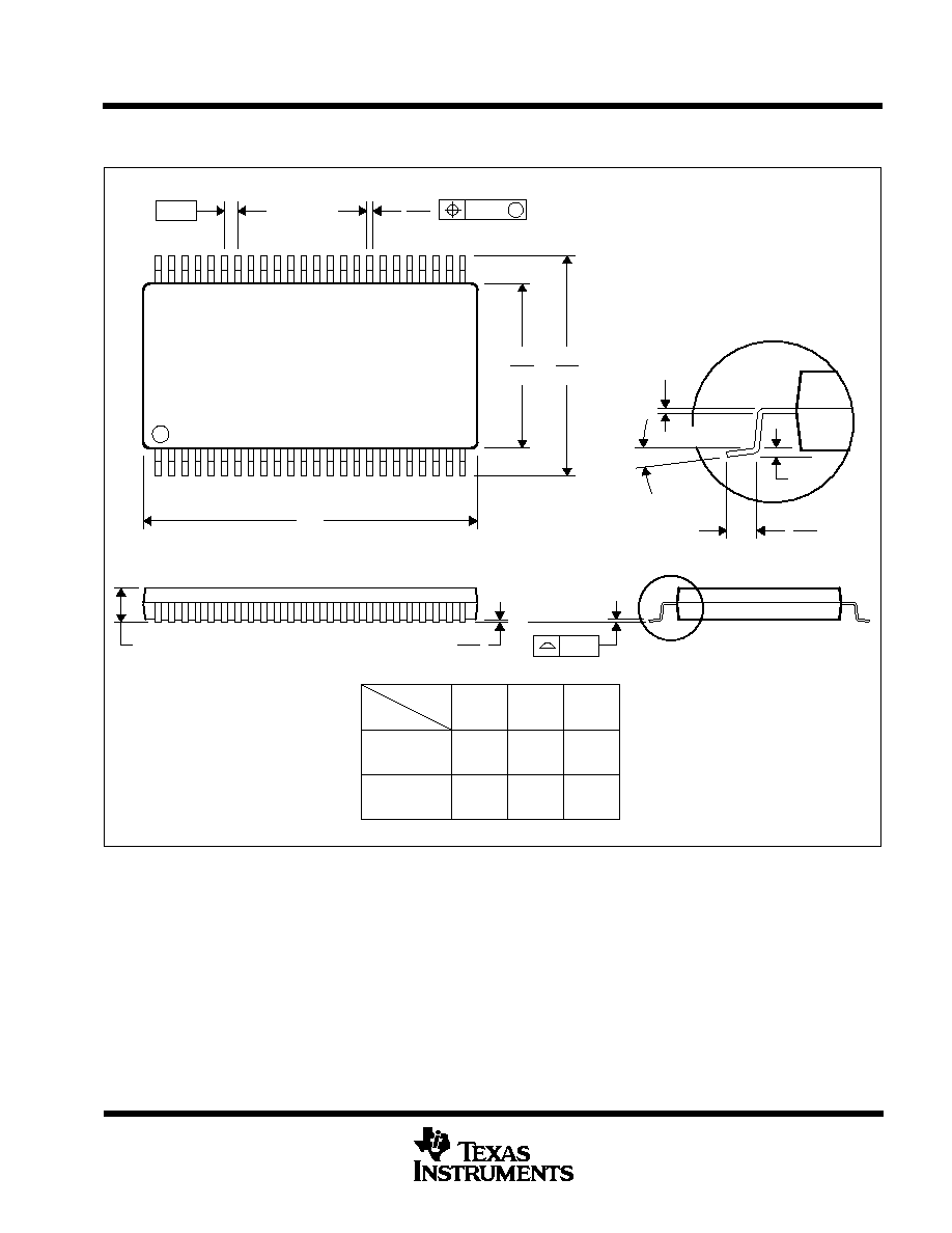
MECHANICAL DATA
MSSO001C ≠ JANUARY 1995 ≠ REVISED DECEMBER 2001
POST OFFICE BOX 655303
∑
DALLAS, TEXAS 75265
DL (R-PDSO-G**)
PLASTIC SMALL-OUTLINE PACKAGE
4040048 / E 12/01
48 PINS SHOWN
56
0.730
(18,54)
0.720
(18,29)
48
28
0.370
(9,40)
(9,65)
0.380
Gage Plane
DIM
0.420 (10,67)
0.395 (10,03)
A MIN
A MAX
0.010 (0,25)
PINS **
0.630
(16,00)
(15,75)
0.620
0.010 (0,25)
Seating Plane
0.020 (0,51)
0.040 (1,02)
25
24
0.008 (0,203)
0.0135 (0,343)
48
1
0.008 (0,20) MIN
A
0.110 (2,79) MAX
0.299 (7,59)
0.291 (7,39)
0.004 (0,10)
M
0.005 (0,13)
0.025 (0,635)
0
∞
≠ 8
∞
0.005 (0,13)
NOTES: A. All linear dimensions are in inches (millimeters).
B. This drawing is subject to change without notice.
C. Body dimensions do not include mold flash or protrusion not to exceed 0.006 (0,15).
D. Falls within JEDEC MO-118
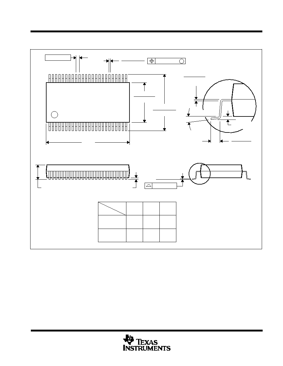
MECHANICAL DATA
MTSS003D ≠ JANUARY 1995 ≠ REVISED JANUARY 1998
POST OFFICE BOX 655303
∑
DALLAS, TEXAS 75265
DGG (R-PDSO-G**)
PLASTIC SMALL-OUTLINE PACKAGE
4040078 / F 12/97
48 PINS SHOWN
0,25
0,15 NOM
Gage Plane
6,00
6,20
8,30
7,90
0,75
0,50
Seating Plane
25
0,27
0,17
24
A
48
1
1,20 MAX
M
0,08
0,10
0,50
0
∞
≠ 8
∞
56
14,10
13,90
48
DIM
A MAX
A MIN
PINS **
12,40
12,60
64
17,10
16,90
0,15
0,05
NOTES: A. All linear dimensions are in millimeters.
B. This drawing is subject to change without notice.
C. Body dimensions do not include mold protrusion not to exceed 0,15.
D. Falls within JEDEC MO-153

IMPORTANT NOTICE
Texas Instruments Incorporated and its subsidiaries (TI) reserve the right to make corrections, modifications,
enhancements, improvements, and other changes to its products and services at any time and to discontinue
any product or service without notice. Customers should obtain the latest relevant information before placing
orders and should verify that such information is current and complete. All products are sold subject to TI's terms
and conditions of sale supplied at the time of order acknowledgment.
TI warrants performance of its hardware products to the specifications applicable at the time of sale in
accordance with TI's standard warranty. Testing and other quality control techniques are used to the extent TI
deems necessary to support this warranty. Except where mandated by government requirements, testing of all
parameters of each product is not necessarily performed.
TI assumes no liability for applications assistance or customer product design. Customers are responsible for
their products and applications using TI components. To minimize the risks associated with customer products
and applications, customers should provide adequate design and operating safeguards.
TI does not warrant or represent that any license, either express or implied, is granted under any TI patent right,
copyright, mask work right, or other TI intellectual property right relating to any combination, machine, or process
in which TI products or services are used. Information published by TI regarding third-party products or services
does not constitute a license from TI to use such products or services or a warranty or endorsement thereof.
Use of such information may require a license from a third party under the patents or other intellectual property
of the third party, or a license from TI under the patents or other intellectual property of TI.
Reproduction of information in TI data books or data sheets is permissible only if reproduction is without
alteration and is accompanied by all associated warranties, conditions, limitations, and notices. Reproduction
of this information with alteration is an unfair and deceptive business practice. TI is not responsible or liable for
such altered documentation.
Resale of TI products or services with statements different from or beyond the parameters stated by TI for that
product or service voids all express and any implied warranties for the associated TI product or service and
is an unfair and deceptive business practice. TI is not responsible or liable for any such statements.
Following are URLs where you can obtain information on other Texas Instruments products and application
solutions:
Products
Applications
Amplifiers
amplifier.ti.com
Audio
www.ti.com/audio
Data Converters
dataconverter.ti.com
Automotive
www.ti.com/automotive
DSP
dsp.ti.com
Broadband
www.ti.com/broadband
Interface
interface.ti.com
Digital Control
www.ti.com/digitalcontrol
Logic
logic.ti.com
Military
www.ti.com/military
Power Mgmt
power.ti.com
Optical Networking
www.ti.com/opticalnetwork
Microcontrollers
microcontroller.ti.com
Security
www.ti.com/security
Telephony
www.ti.com/telephony
Video & Imaging
www.ti.com/video
Wireless
www.ti.com/wireless
Mailing Address:
Texas Instruments
Post Office Box 655303 Dallas, Texas 75265
Copyright
2005, Texas Instruments Incorporated